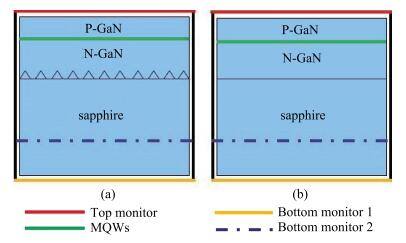
Processing math: 100%
J. Semicond. > 2016, Volume 37 > Issue 10 > 104003

SEMICONDUCTOR DEVICES

Increased effective reflection and transmission at the GaN-sapphire interface of LEDs grown on patterned sapphire substrates

Dongxue Wu1, 2, 3, Ping Ma1, 2, 3, , Boting Liu1, 2, 3, Shuo Zhang1, 2, 3, Junxi Wang1, 2, 3 and Jinmin Li1, 2, 3

+ Author Affiliations

 Corresponding author: Ma Ping, maping@semi.ac.cn

DOI: 10.1088/1674-4926/37/10/104003

PDF

Abstract: The effect of patterned sapphire substrate (PSS) on the top-surface (P-GaN-surface) and the bottom-surface (sapphire-surface) of the light output power (LOP) of GaN-based LEDs was investigated, in order to study the changes in reflection and transmission of the GaN-sapphire interface. Experimental research and computer simulations were combined to reveal a great enhancement in LOP from either the top or bottom surface of GaN-based LEDs, which are prepared on patterned sapphire substrates (PSS-LEDs). Furthermore, the results were compared to those of the conventional LEDs prepared on the planar sapphire substrates (CSS-LEDs). A detailed theoretical analysis was also presented to further support the explanation for the increase in both the effective reflection and transmission of PSS-GaN interface layers and to explain the causes of increased LOP values. Moreover, the bottom-surface of the PSS-LED chip shows slightly increased light output performance when compared to that of the top-surface. Therefore, the light extraction efficiency (LEE) can be further enhanced by integrating the method of PSS and flip-chip structure design.

Key words: light output powertransmissioneffective reflectionpatterned sapphire substratelight-emitting diodes

Nowadays, in order to obtain high brightness in GaN-based LEDs, many methods have been widely adopted, including photonic crystal, surface texturing, PSS, flip-chip and vertical structure[1]. The PSS method has been attracting considerable attention due to its high luminous efficiency[2]. This is because it is an effective and popular method to enhance both internal quantum efficiency (IQE), by reducing threading dislocations (TDs) density and improving the crystalline quality[3-5], and light extraction efficiency (LEE), simultaneously[6]. Due to the substantial difference in refractive index between the epitaxial GaN film and air, the relatively small total internal reflection angle leads to poor LEE[7]. Hence, the patterns can serve as scattering centers for redirecting the guided light into a randomized distribution of angles that will enable multiple entries of photons into the escape cone[8, 9]. This means that, in face-up LED structures, the light scattering effect from the patterns explains very well the enhanced top-surface light output power (LOP) and LEE[10, 11]. Yet, limited research studies have been focused on the investigation of the change in optical parameters, such as reflection coefficient and transmission coefficient. The transmission coefficient is of great importance as it is the key feature to decide whether it is feasible to utilize the PSS technique in flip-chip structures, in order to obtain higher luminous efficiency.

In this study, the results of both experimental research and computer simulations reveal a great enhancement in LOP from either the top or bottom surface of PSS-LEDs, compared to CSS-LEDs. Following that, a theoretical analysis, which is based on two fundamental theories, i.e. the Fresnel Equations and geometrical optics, was performed in order to demonstrate the increase in effective reflection and transmission at the GaN-sapphire interface, which will explain the enhancement in LOP from both the top and bottom surface of PSS-LEDs. Here, it is necessary to clarify that the new term ``effective reflection'' is different from the ``total internal reflection''. The effectively reflected light refers to the amount of light that is reflected and then successfully escapes from the top-surface of the LED. This excludes the total internal reflection light, which cannot radiate out of the LED devices and is eventually absorbed by the LED[12]. As an overall comment, due to the existence of PSS the total internal reflection light that is ultimately absorbed decreases, however, the effective reflection light and the transmission light increase. The increased effective reflection light and the transmission light that can radiate out from top-surface and bottom-surface, respectively, contribute to the enhanced top and bottom surface LOP. Furthermore, a mass of PSS-LED chips is used for separately measuring the top-surface and bottom-surface LOP. These experimental results testify that the latter has slightly superior light luminous performance to the former. It is mainly because the critical angle of GaN surface is smaller than the sapphire surface[13]. Therefore, this study not only demonstrates how the PSS technology can improve the LOP of flip-chip and face-up structure LEDs, compared to CSS, but also that the LOP of flip-chip structure PSS-LEDs is superior to the face-up structure.

To better demonstrate the improvement of PSS on the top and bottom LOP, the simulation based on Trace-Pro software is performed. The LED optical simulation models are presented in Figure 1. The models consist of a p-doped GaN layer with a thickness of 0.2 μm, an n-doped GaN layer with a thickness of 4 μm, and the sapphire substrate with a thickness of 150 μm. The interface is a well-ordered array of circular cones with a diameter of 2.58 μm, a height of 1.53 μm and a periodicity of 3 μm. The patterns shape and parameters were set according to the actual chips used in the aftermentioned experiment. Additionally, Figure 1(b) shows the CSS-LED which will serve as a reference in order to reveal the effect of PSS on LOP or LEE.

Figure  1.  (Color online) Schematic illustration of Trace-Pro simulation models: (a) PSS-LED, (b) CSS-LED. 151 × 91 mm2 (96 × 96 DPI2).

The total flux power of MQWs was set at 2 W and the absorption coefficient of the active layer was considered to be 1000 cm1[14]. In Figure 1, the top monitor receives the optical waves that can be extracted from the top-surface and the bottom monitor 1 receives the optical waves that can be extracted from the bottom-surface of the LED. Therefore, the beam flux power absorbed by the top and bottom monitor 1 represent the LOP from the top-surface and bottom-surface of LED, respectively.

As clearly shown in Table 1, when considering either the top-surface or bottom-surface, the LOP of PSS-LED is higher than that of the CSS-LED. Thus, the simulation results indicate that both top and bottom LOP are increased due to the presence of PSS. Also, regardless of the use of either PSS or CSS model, the bottom LOP is always slightly higher than the top LOP. This also illustrates that the light extraction performance of the bottom-surface is slightly superior to the top-surface and that the flip-chip LED has many advantages over the face-up LED devices for obtaining superior luminous efficiency. Also, the bottom monitor 2 is embedded in the sapphire layer. It can receive directly the optical waves that can be transmitted from the GaN-sapphire interface. As can be seen in Table 1, the value of power recorded by monitor 1 is smaller than monitor 2. This is because the transmission light from the GaN-sapphire interface cannot be completely extracted from the sapphire surface because of total internal reflection at the surface. However, the value of power recorded by monitor 2 in the PSS model is larger than in the CSS model. Thus, the result also demonstrates the increased transmission light at PSS interface.

Table  1.  The absorbed power by various monitors.
DownLoad: CSV  | Show Table

Regarding the experimental procedure, a mass of PSS-LED and CSS-LED chips measured the LOP of the top-surface and bottom-surface, by implementing the two different packaging methods. As presented in Figure 2, the PSS patterns are circular cone shaped, with 2.58 μm in diameter, 1.53 μm in height and 3 μm in period, and featuring a hexagonal array. Additionally, according to the cross-sectional SEM images, the inclination angle of patterns was calculated:

Figure  2.  Cross-sectional SEM images of patterns. 127 × 95 mm (256 × 256 DPI2).
sinα=1.531.990.7688,α50.

Regarding micro-PSS, this kind of pattern with the above feature has been widely used for configuration. Many studies demonstrate that cone-shaped PSS show superior output performance over any other shape and that the geometric parameters used are more effective for LEE in terms of the geometry optics[15].

Figure 3 shows the top and bottom LOPs as a function of the injection current, for the LEDs grown on PSS and CSS. Under an injection current value of 20 mA, the bottom and top LOP of the PSS-LEDs and CSS-LEDs were 11.28, 9.11, 6.22, and 5.14 mW, respectively. Compared to CSS, the bottom and top LOP improvement of PSS-LEDs was 81.4% and 77.2%, respectively. In addition, compared to the top surface of the PSS-LED and CSS-LED, the LOP improvement from the bottom surface was 23.8% and 23.5%, respectively. The experimental results demonstrate the LOP values of PSS-LED compared to CSS-LED and the superior light output performance of the bottom-surface compared to the top-surface.

Figure  3.  (Color online) The top and bottom light output power as a function of the injection current for LEDs grown on PSS and CSS.

When a beam of light penetrates an interface, the power is divided into the one that causes reflection and transmission of the light, as illustrated in Figure 4.

Figure  4.  A schematic of the possible interactions of a beam of light with a surface with different refractive indexes. 143 × 112 mm2 (96 × 96 DPI2).

The amount of the two competing power values is decided by the Fresnel Equations[16]. The value of the reflection coefficient is a function of the refractive index, n, and the angle of incidence, θi, based on the Fresnel formula:

R=12{[n1cosθin21(n1n2sinθi)2n1cosθi+n21(n1n2sinθi)2]2fanxiexiantihuan]+[n11(n1n2sinθi)2n2cosθin11(n1n2sinθi)2+n2cosθi]2}.
(1)

With the transmission coefficient it is:

T=1R,
(2)

where n1 is the index of refraction of substrate, and n2 is the refractive index of the incident region. When the light beam arrives at the interface of GaN (n1=2.4) and sapphire (n2=1.7), the R-θi curve that is developed is presented in the Figure 5.

Figure  5.  Reflection coefficient as a function of the incident angle of θi: R-θi curve. 252 × 163 mm2 (96 × 96 DPI2).

The R-θi curve shows that, in the range of 0-30, the reflection coefficient increases gradually with the increase of the incident angle. Remarkably, the reflection coefficient curve hikes from 0.02 to nearly 1, when the incident angle is about to reach the critical angle value of the total internal reflection, about 45. Therefore, the larger the incident angle θi, the larger the reflection coefficient and the smaller the transmission coefficient.

According to Snell's law, the critical angle of total internal reflection is approximately 25 and 45 for the GaN/air and GaN/sapphire interface, respectively[17]. Hence, the light-emitting ray a1 that propagates upwards from the MQWs, with a deflection angle over 25, is totally reflected by the top-surface. In the case of CSS-LEDs, these photons cannot still radiate outside the top-surface since they are completely reflected by the planar sapphire substrates and are eventually absorbed by the MQWs. However, due to the presence of the cone-shaped patterns layer, part of the reflected upwards photons could be scattered and redirected into a randomized distribution of angles, which enables multiple entries of photons into the top escape cone[18, 19]. Therefore, the analysis described above explains the increase of the effective reflection at the expense of the total internal reflection.

Also, when the ray propagates downwards, with the deflection angle θ over 25, it will reach the GaN/PSS interface layer and the incidence angle will change from the original θ to 50-θ, as ray b1 shown in Figure 6. Because the angle θ is over 25, the angle 50-θ is smaller than the angle θ, namely, the incident angle decreases. According to the Rθi curve, the transmission coefficient increases as incident angle decreases. Thus, the realization of the increased transmission photons also comes at the expense of absorption photons that were originally completely reflected by the CSS-LEDs chip. Especially for the light beams with a deflection angle over 45, the total internal reflection will occur not only on the GaN/air interface but also on the GaN/CSS interface[20] without the use of patterning. Therefore, these photons are less likely to radiate outside the surface and will be eventually absorbed. However, when this part of the ray is incident on the inclined planes of the patterns, the incident angle is significantly reduced. Hence, the part of the total internal reflection ray that was originally absorbed is transformed into large amounts of transmitted light.

Figure  6.  A schematic ray-tracing of light. 254 × 190 mm (96 × 96 DPI).

The ray that arrives at the GaN/sapphire interface layer is divided into three categories, i.e. the effective reflection light that can radiate outside the top-surface, the total internal reflection light that will mainly be absorbed, and the transmission light that can radiate outside the bottom-surface. Due to the existence of patterned sapphire substrates, the absorbed light decreases and is mainly transformed into transmission light and light with more effective reflection. Thus, the enhancement of top and bottom LOP is a fact, due to the increase in effective reflection and transmission of GaN/sapphire interface. In addition, with either the PSS-LEDs or CSS-LEDs, the bottom-surface shows superior luminous performance, when compared to the top-surface. Therefore, the LEE can be further enhanced by integrating the method of patterned sapphire substrates and flip-chip structure design.


[1]
Wang L, Zhang Y, Li X, et al. Partially sandwiched graphene as transparent conductive layer for InGaN-based vertical light emitting diodes. Appl Phys Lett, 2012, 101(6): 061102 doi: 10.1063/1.4742892
[2]
Zhang Y, Wei T, Wang J, et al. The improvement of GaN-based light-emitting diodes using nanopatterned sapphire substrate with small pattern spacing. AIP Advances, 2014, 4(2): 027123 doi: 10.1063/1.4867091
[3]
Kim H G, Na M G, Kim H K, et al. Effect of periodic deflector embedded in InGaN/GaN light emitting diode. Appl Phys Lett, 2007, 90(26): 261117 doi: 10.1063/1.2752777
[4]
Lee Y J, Hsu T C, Kuo H C, et al. Improvement in light-output efficiency of near-ultraviolet InGaN-GaN LEDs fabricated on stripe patterned sapphire substrates. Mater Sci Eng B, 2005, 122(3): 184 doi: 10.1016/j.mseb.2005.05.019
[5]
Wu D S, Wang W K, Wen K S, et al. Defect reduction and efficiency improvement of near-ultraviolet emitters via laterally overgrown GaN on a GaN/patterned sapphire template. Appl Phys Lett, 2006, 89(16): 161105 doi: 10.1063/1.2363148
[6]
Cui H, Park S H. Numerical simulations of light-extraction efficiencies of light-emitting diodes on micro and nanopatterned sapphire substrates. Micro Nano Lett, 2014, 9(12): 841 doi: 10.1049/mnl.2014.0373
[7]
Du C, Wei T, Zheng H, et al. Size-controllable nanopyramids photonic crystal selectively grown on p-GaN for enhanced light-extraction of light-emitting diodes. Opt Express, 2013, 21(21): 25373 doi: 10.1364/OE.21.025373
[8]
Yamada M, Mitani T, Narukawa Y, et al. InGaN-based near-ultraviolet and blue-light-emitting diodes with high external quantum efficiency using a patterned sapphire substrate and a mesh electrode. Jpn J Appl Phys, 2002, 41(12B): L1431
[9]
Tadatomo K, Okagawa H, Ohuchi Y, et al. High output power near-ultraviolet and violet light-emitting diodes fabricated on patterned sapphire substrates using metalorganic vapor phase epitaxy. Third International Conference on Solid State Lighting, 2004: 243
[10]
Wang C C, Ku H, Liu C C, et al. Enhancement of the light output performance for GaN-based light-emitting diodes by bottom pillar structure. Appl Phys Lett, 2007, 91(12): 121109 doi: 10.1063/1.2786015
[11]
Gao H, Yan F, Zhang Y, et al. Enhancement of the light output power of InGaN/GaN light-emitting diodes grown on pyramidal patterned sapphire substrates in the micro-and nanoscale. J Appl Phys, 2008, 103(1): 014314 doi: 10.1063/1.2830981
[12]
Cuong T V, Cheong H S, Kim H G, et al. Enhanced light output from aligned micropit InGaN-based light emitting diodes using wet-etch sapphire patterning. Appl Phys Lett, 2007, 90(13): 131107 doi: 10.1063/1.2714203
[13]
An Tielei, Sun Bo, Wei Tongbo, et al. Light-extraction enhancement of freestanding GaN-based flip-chip light-emitting diodes using two-step roughening methods. Journal of Semiconductors, 2013, 34(11): 114006 doi: 10.1088/1674-4926/34/11/114006
[14]
Pan J W, Tsai P J, Chang K D, et al. Light extraction efficiency analysis of GaN-based light-emitting diodes with nanopatterned sapphire substrates. Appl Opt, 2013, 52(7): 1358 doi: 10.1364/AO.52.001358
[15]
Lee J H, Oh J T, Kim Y C, et al. Stress reduction and enhanced extraction efficiency of GaN-based LED grown on cone-shape-patterned sapphire. IEEE Photon Technol Lett, 2008, 20(17-20): 1563
[16]
Skaar J. Fresnel equations and the refractive index of active media. Phys Rev E, 2006, 73(2): 026605 doi: 10.1103/PhysRevE.73.026605
[17]
Ding Q A, Li K, Kong F, et al. Improving the vertical light extraction efficiency of GaN-based thin-film flip-chip LED with double embedded photonic crystals. IEEE J Quantum Electron, 2015, 51(2): 1
[18]
Lee Y J, Kuo H C, Lu T C, et al. Fabrication and characterization of GaN-based LEDs grown on chemical wet-etched patterned sapphire substrates. J Electrochem Soc, 2006, 153(12): G1106 doi: 10.1149/1.2359701
[19]
Lee T X, Lin C Y, Ma S H, et al. Analysis of position-dependent light extraction of GaN-based LEDs. Opt Express, 2005, 13(11): 4175 doi: 10.1364/OPEX.13.004175
[20]
Chen Maoxing, Xu Chen, Xu Kun, et al. Thermal simulation and analysis of flat surface flip-chip high power light-emitting diodes. Journal of Semiconductors, 2013, 34(12): 124005 doi: 10.1088/1674-4926/34/12/124005
Fig. 1.  (Color online) Schematic illustration of Trace-Pro simulation models: (a) PSS-LED, (b) CSS-LED. 151 × 91 mm2 (96 × 96 DPI2).

Fig. 2.  Cross-sectional SEM images of patterns. 127 × 95 mm (256 × 256 DPI2).

Fig. 3.  (Color online) The top and bottom light output power as a function of the injection current for LEDs grown on PSS and CSS.

Fig. 4.  A schematic of the possible interactions of a beam of light with a surface with different refractive indexes. 143 × 112 mm2 (96 × 96 DPI2).

Fig. 5.  Reflection coefficient as a function of the incident angle of θi: R-θi curve. 252 × 163 mm2 (96 × 96 DPI2).

Fig. 6.  A schematic ray-tracing of light. 254 × 190 mm (96 × 96 DPI).

Table 1.   The absorbed power by various monitors.

[1]
Wang L, Zhang Y, Li X, et al. Partially sandwiched graphene as transparent conductive layer for InGaN-based vertical light emitting diodes. Appl Phys Lett, 2012, 101(6): 061102 doi: 10.1063/1.4742892
[2]
Zhang Y, Wei T, Wang J, et al. The improvement of GaN-based light-emitting diodes using nanopatterned sapphire substrate with small pattern spacing. AIP Advances, 2014, 4(2): 027123 doi: 10.1063/1.4867091
[3]
Kim H G, Na M G, Kim H K, et al. Effect of periodic deflector embedded in InGaN/GaN light emitting diode. Appl Phys Lett, 2007, 90(26): 261117 doi: 10.1063/1.2752777
[4]
Lee Y J, Hsu T C, Kuo H C, et al. Improvement in light-output efficiency of near-ultraviolet InGaN-GaN LEDs fabricated on stripe patterned sapphire substrates. Mater Sci Eng B, 2005, 122(3): 184 doi: 10.1016/j.mseb.2005.05.019
[5]
Wu D S, Wang W K, Wen K S, et al. Defect reduction and efficiency improvement of near-ultraviolet emitters via laterally overgrown GaN on a GaN/patterned sapphire template. Appl Phys Lett, 2006, 89(16): 161105 doi: 10.1063/1.2363148
[6]
Cui H, Park S H. Numerical simulations of light-extraction efficiencies of light-emitting diodes on micro and nanopatterned sapphire substrates. Micro Nano Lett, 2014, 9(12): 841 doi: 10.1049/mnl.2014.0373
[7]
Du C, Wei T, Zheng H, et al. Size-controllable nanopyramids photonic crystal selectively grown on p-GaN for enhanced light-extraction of light-emitting diodes. Opt Express, 2013, 21(21): 25373 doi: 10.1364/OE.21.025373
[8]
Yamada M, Mitani T, Narukawa Y, et al. InGaN-based near-ultraviolet and blue-light-emitting diodes with high external quantum efficiency using a patterned sapphire substrate and a mesh electrode. Jpn J Appl Phys, 2002, 41(12B): L1431
[9]
Tadatomo K, Okagawa H, Ohuchi Y, et al. High output power near-ultraviolet and violet light-emitting diodes fabricated on patterned sapphire substrates using metalorganic vapor phase epitaxy. Third International Conference on Solid State Lighting, 2004: 243
[10]
Wang C C, Ku H, Liu C C, et al. Enhancement of the light output performance for GaN-based light-emitting diodes by bottom pillar structure. Appl Phys Lett, 2007, 91(12): 121109 doi: 10.1063/1.2786015
[11]
Gao H, Yan F, Zhang Y, et al. Enhancement of the light output power of InGaN/GaN light-emitting diodes grown on pyramidal patterned sapphire substrates in the micro-and nanoscale. J Appl Phys, 2008, 103(1): 014314 doi: 10.1063/1.2830981
[12]
Cuong T V, Cheong H S, Kim H G, et al. Enhanced light output from aligned micropit InGaN-based light emitting diodes using wet-etch sapphire patterning. Appl Phys Lett, 2007, 90(13): 131107 doi: 10.1063/1.2714203
[13]
An Tielei, Sun Bo, Wei Tongbo, et al. Light-extraction enhancement of freestanding GaN-based flip-chip light-emitting diodes using two-step roughening methods. Journal of Semiconductors, 2013, 34(11): 114006 doi: 10.1088/1674-4926/34/11/114006
[14]
Pan J W, Tsai P J, Chang K D, et al. Light extraction efficiency analysis of GaN-based light-emitting diodes with nanopatterned sapphire substrates. Appl Opt, 2013, 52(7): 1358 doi: 10.1364/AO.52.001358
[15]
Lee J H, Oh J T, Kim Y C, et al. Stress reduction and enhanced extraction efficiency of GaN-based LED grown on cone-shape-patterned sapphire. IEEE Photon Technol Lett, 2008, 20(17-20): 1563
[16]
Skaar J. Fresnel equations and the refractive index of active media. Phys Rev E, 2006, 73(2): 026605 doi: 10.1103/PhysRevE.73.026605
[17]
Ding Q A, Li K, Kong F, et al. Improving the vertical light extraction efficiency of GaN-based thin-film flip-chip LED with double embedded photonic crystals. IEEE J Quantum Electron, 2015, 51(2): 1
[18]
Lee Y J, Kuo H C, Lu T C, et al. Fabrication and characterization of GaN-based LEDs grown on chemical wet-etched patterned sapphire substrates. J Electrochem Soc, 2006, 153(12): G1106 doi: 10.1149/1.2359701
[19]
Lee T X, Lin C Y, Ma S H, et al. Analysis of position-dependent light extraction of GaN-based LEDs. Opt Express, 2005, 13(11): 4175 doi: 10.1364/OPEX.13.004175
[20]
Chen Maoxing, Xu Chen, Xu Kun, et al. Thermal simulation and analysis of flat surface flip-chip high power light-emitting diodes. Journal of Semiconductors, 2013, 34(12): 124005 doi: 10.1088/1674-4926/34/12/124005
1

Light-emitting diodes based on all-inorganic copper halide perovskite with self-trapped excitons

Nian Liu, Xue Zhao, Mengling Xia, Guangda Niu, Qingxun Guo, et al.

Journal of Semiconductors, 2020, 41(5): 052204. doi: 10.1088/1674-4926/41/5/052204

2

The strategies for preparing blue perovskite light-emitting diodes

Jianxun Lu, Zhanhua Wei

Journal of Semiconductors, 2020, 41(5): 051203. doi: 10.1088/1674-4926/41/5/051203

3

Giant efficiency and color purity enhancement in multicolor inorganic perovskite light-emitting diodes via heating-assisted vacuum deposition

Boning Han, Qingsong Shan, Fengjuan Zhang, Jizhong Song, Haibo Zeng, et al.

Journal of Semiconductors, 2020, 41(5): 052205. doi: 10.1088/1674-4926/41/5/052205

4

Rational molecular passivation for high-performance perovskite light-emitting diodes

Jingbi You

Journal of Semiconductors, 2019, 40(4): 040203. doi: 10.1088/1674-4926/40/4/040203

5

A monolithic integrated low-voltage deep brain stimulator with wireless power and data transmission

Zhang Zhang, Ye Tan, Jianmin Zeng, Xu Han, Xin Cheng, et al.

Journal of Semiconductors, 2016, 37(9): 095003. doi: 10.1088/1674-4926/37/9/095003

6

Evaluation of light extraction efficiency for the light-emitting diodes based on the transfer matrix formalism and ray-tracing method

Pingbo An, Li Wang, Hongxi Lu, Zhiguo Yu, Lei Liu, et al.

Journal of Semiconductors, 2016, 37(6): 064015. doi: 10.1088/1674-4926/37/6/064015

7

Enhancement of blue InGaN light-emitting diodes by using AlGaN increased composition-graded barriers

Yan Lei, Zhiqiang Liu, Miao He, Xiaoyan Yi, Junxi Wang, et al.

Journal of Semiconductors, 2015, 36(5): 054006. doi: 10.1088/1674-4926/36/5/054006

8

Enhanced electroluminescence from a free-standing tensilely strained germanium nanomembrane light-emitting diode

Jingming Chen, Bin Shu, Jibao Wu, Linxi Fan, Heming Zhang, et al.

Journal of Semiconductors, 2015, 36(10): 104004. doi: 10.1088/1674-4926/36/10/104004

9

Performance analysis of silicon nanowire transistors considering effective oxide thickness of high-k gate dielectric

S. Theodore Chandra, N. B. Balamurugan

Journal of Semiconductors, 2014, 35(4): 044001. doi: 10.1088/1674-4926/35/4/044001

10

GaN-based light-emitting diodes with hybrid micro/nano-textured indium-tin-oxide layer

Huamao Huang, Jinyong Hu, Hong Wang

Journal of Semiconductors, 2014, 35(8): 084006. doi: 10.1088/1674-4926/35/8/084006

11

Enhanced performance of InGaN/GaN multiple quantum well solar cells with patterned sapphire substrate

Liang Jing, Hongling Xiao, Xiaoliang Wang, Cuimei Wang, Qingwen Deng, et al.

Journal of Semiconductors, 2013, 34(12): 124004. doi: 10.1088/1674-4926/34/12/124004

12

Spacing optimization of high power LED arrays for solid state lighting

Y. Sing Chan, S. W. Ricky Lee

Journal of Semiconductors, 2011, 32(1): 014005. doi: 10.1088/1674-4926/32/1/014005

13

Degradation of light emitting diodes: a proposed methodology

Sau Koh, Willem Van Driel, G. Q. Zhang

Journal of Semiconductors, 2011, 32(1): 014004. doi: 10.1088/1674-4926/32/1/014004

14

Improved III-nitrides based light-emitting diodes anti-electrostatic discharge capacity with an AlGaN/GaN stack insert layer

Li Zhicong, Li Panpan, Wang Bing, Li Hongjian, Liang Meng, et al.

Journal of Semiconductors, 2011, 32(11): 114007. doi: 10.1088/1674-4926/32/11/114007

15

Current–voltage characteristics of light-emitting diodes under optical and electrical excitation

Wen Jing, Wen Yumei, Li Ping, Li Lian

Journal of Semiconductors, 2011, 32(8): 084004. doi: 10.1088/1674-4926/32/8/084004

16

Fluorescent SiC and its application to white light-emitting diodes

Satoshi Kamiyama, Motoaki Iwaya, Tetsuya Takeuchi, Isamu Akasaki, Mikael Syvajarvi, et al.

Journal of Semiconductors, 2011, 32(1): 013004. doi: 10.1088/1674-4926/32/1/013004

17

Properties of the ITO layer in a novel red light-emitting diode

Zhang Yonghui, Guo Weiling, Gao Wei, Li Chunwei, Ding Tianping, et al.

Journal of Semiconductors, 2010, 31(4): 043002. doi: 10.1088/1674-4926/31/4/043002

18

Room-temperature electroluminescence of p-ZnxMg1-xO:Na/n-ZnO p-n junction light emitting diode

Ye Zhizhen, Zhang Liqiang, Huang Jingyun, Zhang Yinzhu, Zhu Liping, et al.

Journal of Semiconductors, 2009, 30(8): 081001. doi: 10.1088/1674-4926/30/8/081001

19

High-Power Distributed Feedback Laser Diodes Emitting at 820nm

Fu Shenghui, Zhong Yuan, Song Guofeng, Chen Lianghui

Chinese Journal of Semiconductors , 2006, 27(6): 966-969.

20

Fabrication and Emission Properties of a n-ZnO/p-GaN Heterojunction Light-Emitting Diode

Zhou Xin, Gu Shulin, Zhu Shunming, Ye Jiandong, Liu Wei, et al.

Chinese Journal of Semiconductors , 2006, 27(2): 249-253.

1. Liu, S., Yang, J., Zhao, D. et al. Uniform-Sized Indium Quantum Dots Grown on the Surface of an InGaN Epitaxial Layer by a Two-Step Cooling Process. Nanoscale Research Letters, 2019, 14(1): 280. doi:10.1186/s11671-019-3095-7
2. Wang, J., Tao, Q., Hu, C. et al. Fabrication of sapphire rib waveguides using a femtosecond laser. Optoelectronics Letters, 2019, 15(3): 190-194. doi:10.1007/s11801-019-8180-8
3. Liu, S.T., Yang, J., Zhao, D.G. et al. The compensation role of deep defects in the electric properties of lightly Si-doped GaN. Journal of Alloys and Compounds, 2019. doi:10.1016/j.jallcom.2018.09.333
4. Liu, S.-T., Yang, J., Zhao, D.-G. et al. Influence of carrier gas H2 flow rate on quality of p-type GaN epilayer grown and annealed at lower temperatures. Chinese Physics B, 2018, 27(12): 127803. doi:10.1088/1674-1056/27/12/127803
5. Liu, S.T., Yang, J., Zhao, D.G. et al. The influence of thermal annealing process after GaN cap layer growth on structural and optical properties of InGaN/InGaN multi-quantum wells. Optical Materials, 2018. doi:10.1016/j.optmat.2018.10.034
6. Xing, Y., Zhao, D., Jiang, D. et al. The role of temperature ramp-up time before barrier layer growth in optical and structural properties of InGaN/GaN multi-quantum wells. Superlattices and Microstructures, 2018. doi:10.1016/j.spmi.2018.03.033
7. Liu, W., Zhao, D., Jiang, D. et al. Effect of carrier transfer process between two kinds of localized potential traps on the spectral properties of InGaN/GaN multiple quantum wells. Optics Express, 2018, 26(3): 3424-3434. doi:10.1364/OE.26.003427
8. Liang, F., Zhao, D., Jiang, D. et al. Improvement of Ohmic contact to p-GaN by controlling the residual carbon concentration in p++-GaN layer. Journal of Crystal Growth, 2017. doi:10.1016/j.jcrysgro.2017.03.009
  • Search

    Advanced Search >>

    GET CITATION

    Dongxue Wu, Ping Ma, Boting Liu, Shuo Zhang, Junxi Wang, Jinmin Li. Increased effective reflection and transmission at the GaN-sapphire interface of LEDs grown on patterned sapphire substrates[J]. Journal of Semiconductors, 2016, 37(10): 104003. doi: 10.1088/1674-4926/37/10/104003
    D X Wu, P Ma, B T Liu, S Zhang, J X Wang, J M Li. Increased effective reflection and transmission at the GaN-sapphire interface of LEDs grown on patterned sapphire substrates[J]. J. Semicond., 2016, 37(10): 104003. doi: 10.1088/1674-4926/37/10/104003.
    shu

    Export: BibTex EndNote

    Article Metrics

    Article views: 3041 Times PDF downloads: 25 Times Cited by: 8 Times

    History

    Received: 28 January 2016 Revised: 15 April 2016 Online: Published: 01 October 2016

    Catalog

      Email This Article

      User name:
      Email:*请输入正确邮箱
      Code:*验证码错误
      Dongxue Wu, Ping Ma, Boting Liu, Shuo Zhang, Junxi Wang, Jinmin Li. Increased effective reflection and transmission at the GaN-sapphire interface of LEDs grown on patterned sapphire substrates[J]. Journal of Semiconductors, 2016, 37(10): 104003. doi: 10.1088/1674-4926/37/10/104003 ****D X Wu, P Ma, B T Liu, S Zhang, J X Wang, J M Li. Increased effective reflection and transmission at the GaN-sapphire interface of LEDs grown on patterned sapphire substrates[J]. J. Semicond., 2016, 37(10): 104003. doi: 10.1088/1674-4926/37/10/104003.
      Citation:
      Dongxue Wu, Ping Ma, Boting Liu, Shuo Zhang, Junxi Wang, Jinmin Li. Increased effective reflection and transmission at the GaN-sapphire interface of LEDs grown on patterned sapphire substrates[J]. Journal of Semiconductors, 2016, 37(10): 104003. doi: 10.1088/1674-4926/37/10/104003 ****
      D X Wu, P Ma, B T Liu, S Zhang, J X Wang, J M Li. Increased effective reflection and transmission at the GaN-sapphire interface of LEDs grown on patterned sapphire substrates[J]. J. Semicond., 2016, 37(10): 104003. doi: 10.1088/1674-4926/37/10/104003.

      Increased effective reflection and transmission at the GaN-sapphire interface of LEDs grown on patterned sapphire substrates

      DOI: 10.1088/1674-4926/37/10/104003
      Funds:

      Project supported by the National High Technology Program of China (No.Y48A040000) and the National High Technology Program of China (No.Y48A040000)

      the National High Technology Program of China Y48A040000

      the National High Technology Program of China Y48A040000

      More Information
      • Corresponding author: Ma Ping, maping@semi.ac.cn
      • Received Date: 2016-01-28
      • Revised Date: 2016-04-15
      • Published Date: 2016-10-01

      Catalog

        /

        DownLoad:  Full-Size Img  PowerPoint
        Return
        Return