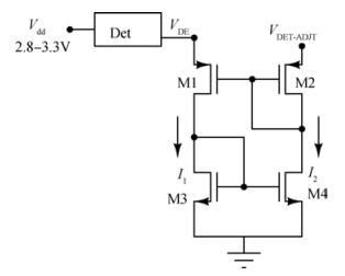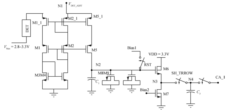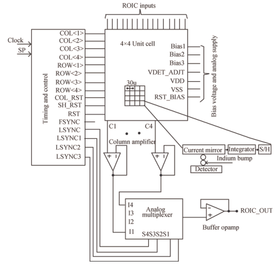
Fig. 1.
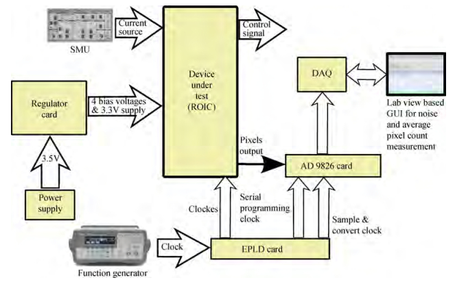
ROIC block diagram.
SEMICONDUCTOR INTEGRATED CIRCUITS
Hari Shanker Gupta1, , A S Kiran Kumar2, M. Shojaei Baghini1, Subhananda Chakrabarti1, Sanjeev Mehta2, Arup Roy Chowdhury2 and Dinesh K Sharma1
Corresponding author: Hari Shanker Gupta, Email: harishanker@ee.iitb.ac.in, harigupta1506@gmail.com
Abstract: Current mirror integration (CMI) read out integrated circuit (ROIC) topology provides a low input impedance to photo-detectors and provides large injection efficiency, large charge handling capacity and snapshot mode operation without in-pixel opamps. The ROIC described in this paper has been implemented with a modified current mirror circuit, with matched PMOS pairs for detector input stage and its biasing. The readout circuit has been designed for 30×30μm2 pixel size, 4×4 array size, variable frame rate, 5 Mega pixel per second (Mpps). Experimental performance of the test chip has achieved 15 Me charge handling capacity, a high dynamic range of 83 dB, 99.8% linearity and 99.96% injection efficiency. The ROIC design has been fabricated in 3.3 V 1P6M UMC 180 nm CMOS process and tested up to 5 MHz pixel rate at room and at cryogenic temperature.
Keywords: pixel pitch, readout integrated circuit (ROIC), cryogenics, snapshot, FPA, IR detectors
| [1] |
Ting D, Gunapala S D. Quantum well and quantum dot modeling for advanced infrared detectors and focal plane arrays. 2nd BEER International Workshop on Space Mission Challenges for Information Technology Pasadena, California, 2006
|
| [2] |
Kulah H, Akin T. A current mirroring integration based readout circuit for high performance infrared FPA applications. IEEE Trans Circuits Syst I, 2003, 50(4): 181 doi: 10.1109/TCSII.2003.807758
|
| [3] |
Vampola J L. The infrared and electro-optical systems handbook. International Society for Optical Engine (SPIE), Billingham, WA, USA, 1993
|
| [4] |
Wu R, Huijsing J H, Makinwa K A A. A 21 b ± 40 mV range read-out IC for bridge transducers. IEEE ISSCC, 2011: 22
|
| [5] |
Johnson J F, Lomheim T S. Focal-plane signal and noise model-CTIA ROIC. IEEE Trans Electron Devices, 2009, 56(11): 2506 doi: 10.1109/TED.2009.2030646
|
| [6] |
Barve A, Lee S J, Noh S K, et al. Review of current progress in quantum dot infrared photodetectors. IEEE Laser Photon Rev, 2009: 1 http://cn.bing.com/academic/profile?id=2079939143&encoded=0&v=paper_preview&mkt=zh-cn
|
| [7] |
Sun T P, Li J H, Lu Y C. Readout circuit with dual switching mode design for infrared focal plane arrays. Infrared Physics Technology, 2014, 65: 9 doi: 10.1016/j.infrared.2014.03.003
|
| [8] |
Johnson J. Hybrid infrared focal plane signal and noise model. IEEE Trans Electron Devices, 1999, 46: 96 doi: 10.1109/16.737447
|
| [9] |
Yoon N, Kim B, Lee H, et al. Design and implementation of infrared readout circuit using new input circuit of current mirroring direct injection (CMDI). Optoelectron Rev, 1999, 7: 321 https://www.researchgate.net/publication/288556189_Design_and_implementation_of_infrared_readout_circuit_using_a_new_input_circuit_of_current_mirroring_direct_injection_CMDI
|
| [10] |
Kayahan H, Ergintav A, Ceylan O, et al. Realization of a ROIC for 72 × 4 PV-IR detectors. Proc SPIE, 2008, 6890: 68900F doi: 10.1117/12.765218
|
| [11] |
Ma Wenlong, Shi Yin, Zhang Yaohui, et al. A snap-shot mode cryogenic readout circuit for QWIP IR FPAs. Journal of Semiconductors, 2010, 31: 025012 doi: 10.1088/1674-4926/31/2/025012
|
| [12] |
Rogalski A. Infrared detectors. 2nd ed. CRC Press, 2010
|
| [13] |
Kang S G, Woo D H, Lee H C. Multiple integration method for a high signal-to-noise ratio readout integrated circuit. IEEE Trans Circuits Syst II, 2005, 52: 553 doi: 10.1109/TCSII.2005.848984
|
| [14] |
Hao Lichao, Ding Ruijun, Zhang Junling, et al. A high-performance readout circuit (ROIC) for VL WIR FPAs with novel current mode background suppression. 2012 International Conference on Measurement, Information and Control (MIC), 2012: 869 http://cn.bing.com/academic/profile?id=2050866612&encoded=0&v=paper_preview&mkt=zh-cn
|
| [15] |
Huang Z Q, Guo F M. Readout design for imagers with non-saturated integrating. 2014 International Conference on Information and Automation and Information, 2014: 1206 http://cn.bing.com/academic/profile?id=2062868502&encoded=0&v=paper_preview&mkt=zh-cn
|
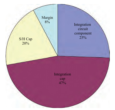
Table 1. Black device performance comparison.
 |
| [1] |
Ting D, Gunapala S D. Quantum well and quantum dot modeling for advanced infrared detectors and focal plane arrays. 2nd BEER International Workshop on Space Mission Challenges for Information Technology Pasadena, California, 2006
|
| [2] |
Kulah H, Akin T. A current mirroring integration based readout circuit for high performance infrared FPA applications. IEEE Trans Circuits Syst I, 2003, 50(4): 181 doi: 10.1109/TCSII.2003.807758
|
| [3] |
Vampola J L. The infrared and electro-optical systems handbook. International Society for Optical Engine (SPIE), Billingham, WA, USA, 1993
|
| [4] |
Wu R, Huijsing J H, Makinwa K A A. A 21 b ± 40 mV range read-out IC for bridge transducers. IEEE ISSCC, 2011: 22
|
| [5] |
Johnson J F, Lomheim T S. Focal-plane signal and noise model-CTIA ROIC. IEEE Trans Electron Devices, 2009, 56(11): 2506 doi: 10.1109/TED.2009.2030646
|
| [6] |
Barve A, Lee S J, Noh S K, et al. Review of current progress in quantum dot infrared photodetectors. IEEE Laser Photon Rev, 2009: 1 http://cn.bing.com/academic/profile?id=2079939143&encoded=0&v=paper_preview&mkt=zh-cn
|
| [7] |
Sun T P, Li J H, Lu Y C. Readout circuit with dual switching mode design for infrared focal plane arrays. Infrared Physics Technology, 2014, 65: 9 doi: 10.1016/j.infrared.2014.03.003
|
| [8] |
Johnson J. Hybrid infrared focal plane signal and noise model. IEEE Trans Electron Devices, 1999, 46: 96 doi: 10.1109/16.737447
|
| [9] |
Yoon N, Kim B, Lee H, et al. Design and implementation of infrared readout circuit using new input circuit of current mirroring direct injection (CMDI). Optoelectron Rev, 1999, 7: 321 https://www.researchgate.net/publication/288556189_Design_and_implementation_of_infrared_readout_circuit_using_a_new_input_circuit_of_current_mirroring_direct_injection_CMDI
|
| [10] |
Kayahan H, Ergintav A, Ceylan O, et al. Realization of a ROIC for 72 × 4 PV-IR detectors. Proc SPIE, 2008, 6890: 68900F doi: 10.1117/12.765218
|
| [11] |
Ma Wenlong, Shi Yin, Zhang Yaohui, et al. A snap-shot mode cryogenic readout circuit for QWIP IR FPAs. Journal of Semiconductors, 2010, 31: 025012 doi: 10.1088/1674-4926/31/2/025012
|
| [12] |
Rogalski A. Infrared detectors. 2nd ed. CRC Press, 2010
|
| [13] |
Kang S G, Woo D H, Lee H C. Multiple integration method for a high signal-to-noise ratio readout integrated circuit. IEEE Trans Circuits Syst II, 2005, 52: 553 doi: 10.1109/TCSII.2005.848984
|
| [14] |
Hao Lichao, Ding Ruijun, Zhang Junling, et al. A high-performance readout circuit (ROIC) for VL WIR FPAs with novel current mode background suppression. 2012 International Conference on Measurement, Information and Control (MIC), 2012: 869 http://cn.bing.com/academic/profile?id=2050866612&encoded=0&v=paper_preview&mkt=zh-cn
|
| [15] |
Huang Z Q, Guo F M. Readout design for imagers with non-saturated integrating. 2014 International Conference on Information and Automation and Information, 2014: 1206 http://cn.bing.com/academic/profile?id=2062868502&encoded=0&v=paper_preview&mkt=zh-cn
|


Article views: 6536 Times PDF downloads: 61 Times Cited by: 0 Times
Received: 20 January 2016 Revised: 18 May 2016 Online: Published: 01 October 2016
| Citation: |
Hari Shanker Gupta, A S Kiran Kumar, M. Shojaei Baghini, Subhananda Chakrabarti, Sanjeev Mehta, Arup Roy Chowdhury, Dinesh K Sharma. Design of current mirror integration ROIC for snapshot mode operation[J]. Journal of Semiconductors, 2016, 37(10): 105001. doi: 10.1088/1674-4926/37/10/105001
****
H S Gupta, A S K Kumar, M. S. Baghini, S. Chakrabarti, S Mehta, A R Chowdhury, D K Sharma. Design of current mirror integration ROIC for snapshot mode operation[J]. J. Semicond., 2016, 37(10): 105001. doi: 10.1088/1674-4926/37/10/105001.

|
| [1] |
Ting D, Gunapala S D. Quantum well and quantum dot modeling for advanced infrared detectors and focal plane arrays. 2nd BEER International Workshop on Space Mission Challenges for Information Technology Pasadena, California, 2006
|
| [2] |
Kulah H, Akin T. A current mirroring integration based readout circuit for high performance infrared FPA applications. IEEE Trans Circuits Syst I, 2003, 50(4): 181 doi: 10.1109/TCSII.2003.807758
|
| [3] |
Vampola J L. The infrared and electro-optical systems handbook. International Society for Optical Engine (SPIE), Billingham, WA, USA, 1993
|
| [4] |
Wu R, Huijsing J H, Makinwa K A A. A 21 b ± 40 mV range read-out IC for bridge transducers. IEEE ISSCC, 2011: 22
|
| [5] |
Johnson J F, Lomheim T S. Focal-plane signal and noise model-CTIA ROIC. IEEE Trans Electron Devices, 2009, 56(11): 2506 doi: 10.1109/TED.2009.2030646
|
| [6] |
Barve A, Lee S J, Noh S K, et al. Review of current progress in quantum dot infrared photodetectors. IEEE Laser Photon Rev, 2009: 1 http://cn.bing.com/academic/profile?id=2079939143&encoded=0&v=paper_preview&mkt=zh-cn
|
| [7] |
Sun T P, Li J H, Lu Y C. Readout circuit with dual switching mode design for infrared focal plane arrays. Infrared Physics Technology, 2014, 65: 9 doi: 10.1016/j.infrared.2014.03.003
|
| [8] |
Johnson J. Hybrid infrared focal plane signal and noise model. IEEE Trans Electron Devices, 1999, 46: 96 doi: 10.1109/16.737447
|
| [9] |
Yoon N, Kim B, Lee H, et al. Design and implementation of infrared readout circuit using new input circuit of current mirroring direct injection (CMDI). Optoelectron Rev, 1999, 7: 321 https://www.researchgate.net/publication/288556189_Design_and_implementation_of_infrared_readout_circuit_using_a_new_input_circuit_of_current_mirroring_direct_injection_CMDI
|
| [10] |
Kayahan H, Ergintav A, Ceylan O, et al. Realization of a ROIC for 72 × 4 PV-IR detectors. Proc SPIE, 2008, 6890: 68900F doi: 10.1117/12.765218
|
| [11] |
Ma Wenlong, Shi Yin, Zhang Yaohui, et al. A snap-shot mode cryogenic readout circuit for QWIP IR FPAs. Journal of Semiconductors, 2010, 31: 025012 doi: 10.1088/1674-4926/31/2/025012
|
| [12] |
Rogalski A. Infrared detectors. 2nd ed. CRC Press, 2010
|
| [13] |
Kang S G, Woo D H, Lee H C. Multiple integration method for a high signal-to-noise ratio readout integrated circuit. IEEE Trans Circuits Syst II, 2005, 52: 553 doi: 10.1109/TCSII.2005.848984
|
| [14] |
Hao Lichao, Ding Ruijun, Zhang Junling, et al. A high-performance readout circuit (ROIC) for VL WIR FPAs with novel current mode background suppression. 2012 International Conference on Measurement, Information and Control (MIC), 2012: 869 http://cn.bing.com/academic/profile?id=2050866612&encoded=0&v=paper_preview&mkt=zh-cn
|
| [15] |
Huang Z Q, Guo F M. Readout design for imagers with non-saturated integrating. 2014 International Conference on Information and Automation and Information, 2014: 1206 http://cn.bing.com/academic/profile?id=2062868502&encoded=0&v=paper_preview&mkt=zh-cn
|

 WeChat ID
Journal of Semiconductors © 2017 All Rights Reserved 京ICP备05085259号-2

 DownLoad: