Fig. 1.
(Color online) Radiation-induced leakage path in a modern CMOS technology.
SEMICONDUCTOR DEVICES
Baoping He, Zujun Wang, Jiangkun Sheng and Shaoyan Huang
Corresponding author: Wang Zujun, Email:wangzujun@nint.ac.cn
Abstract: In this paper, total ionizing dose effect of NMOS transistors in advanced CMOS technology are examined. The radiation tests are performed at 60Co sources at the dose rate of 50 rad (Si)/s. The investigation's results show that the radiation-induced charge buildup in the gate oxide can be ignored, and the field oxide isolation structure is the main total dose problem. The total ionizing dose (TID) radiation effects of field oxide parasitic transistors are studied in detail. An analytical model of radiation defect charge induced by TID damage in field oxide is established. The I-V characteristics of the NMOS parasitic transistors at different doses are modeled by using a surface potential method. The modeling method is verified by the experimental I-V characteristics of 180 nm commercial NMOS device induced by TID radiation at different doses. The model results are in good agreement with the radiation experimental results, which shows the analytical model can accurately predict the radiation response characteristics of advanced bulk CMOS technology device.
Keywords: total ionizing dose (TID), bulk CMOS, shallow trench isolation (STI), oxide trapped charge, interface traps
| [1] |
Barnaby H J. Total-ionizing-dose effects in modern CMOS technologies. IEEE Trans Nucl Sci, 2006, 53(6): 3103 doi: 10.1109/TNS.2006.885952
|
| [2] |
McLain M L, Barnaby H J, Holbert K E, et al. Enhanced TID susceptibility in sub-100-nm bulk CMOS I/Otransistors and circuits. IEEE Trans Nucl Sci, 2007, 54(6): 2210 doi: 10.1109/TNS.2007.908461
|
| [3] |
Faccio F, Cervelli G. Radiation-induced edge effects in deep submicron CMOS transistors. IEEE Trans Nucl Sci, 2007, 52(6): 2413 https://www.researchgate.net/publication/3139618_Radiation-induced_edge_effects_in_deep_submicron_CMOS_transistors
|
| [4] |
Ding Lili, Guo Hongxia, Chen Wei, et al. Study of radiation induced leakage current between adjacent devices in a CMOS integrated circuit. Journal of Semiconductors, 2012, 33(6): 064006 doi: 10.1088/1674-4926/33/6/064006
|
| [5] |
Zhao Yuanfu, Zheng Hongchao, Fan Long, et al. Experimental research on transient radiation effects in microprocessors based on SPARC-V8 architecture. Journal of Semiconductors, 2015, 36(11): 114008 doi: 10.1088/1674-4926/36/11/114008
|
| [6] |
Li Leilei, Zhou Xinjie, Yu Zongguang, et al. Effect of phosphorus ion implantation on back gate effect of partially depleted SOI NMOS under total dose radiation. Journal of Semiconductors, 2015, 36(1): 014006 doi: 10.1088/1674-4926/36/1/014006
|
| [7] |
Peng C, Hu Z Y, Zhang Z X, et al. A new method for extracting the radiation induced trapped charge density along the STI sidewall in the PDSOI NMOSFETs. IEEE Trans Nucl Sci, 2013, 60(6): 4697 doi: 10.1109/TNS.2013.2283504
|
| [8] |
H Z Y, Liu Z L, Shao H, et al. Comprehensive study on the total dose effects in a 180-nm CMOS technology. IEEE Trans Nucl Sci, 2011, 58 (3): 1347 doi: 10.1109/TNS.2011.2132145
|
| [9] |
Fleetwood D M. Total ionizing dose effects in MOS and low dose-rate-sensitive linear-bipolar. IEEE Trans Nucl Sci, 2013, 60(3): 1706 doi: 10.1109/TNS.2013.2259260
|
| [10] |
Turowski M, Raman A, Schrimpf R D. Nonuniform total-dose-induced charge distribution in shallow-trench isolation oxides. IEEE Trans Nucl Sci, 2004, 51(6): 3166 doi: 10.1109/TNS.2004.839201
|
| [11] |
Johnston A H, Swimm R T, Allen G R, et al. Total dose effects in CMOS trench isolation regions. IEEE Trans Nucl Sci, 2009, 56(4): 1941 doi: 10.1109/TNS.2009.2019273
|
| [12] |
Esqueda I S, Barnaby H J. Modeling the non-uniform distribution of radiation-induced interface traps. IEEE Trans Nucl Sci, 2012, 59(4): 723 doi: 10.1109/TNS.2012.2186826
|
| [13] |
Tang Zhaohuan, Liu Rongkan, Tan Kaizhou, et al. A novel terminal structure for total dose irradiation hardened of a P-VDMOS. Journal of Semiconductors, 2014, 35(5): 054005 doi: 10.1088/1674-4926/35/5/054005
|
| [14] |
McLean F B. A framework for understanding radiation-induced interface states in SiO2 MOS structures. IEEE Trans Nucl Sci, 1980, 27(6): 1651 doi: 10.1109/TNS.1980.4331084
|
| [15] |
Shaneyfelt M R, Schwank J R, Fleetwood D M, et al. Field dependence of interface-trap buildup in polysilicon and metal gate MOS devices. IEEE Trans Nucl Sci, 1990, 37(6): 1632 doi: 10.1109/23.101171
|
| [16] |
Zhao Qifeng, Zhuang Yiqi, Bao Junlin, et al. Model of radiation induced gain degradation of NPN junction transistor at different dose rates. Journal of Semiconductors, 2015, 36(6): 064007 doi: 10.1088/1674-4926/36/6/064007
|
| [17] |
Zebrev G I, Petrov A S, Useinov R G, et al. Simulation of bipolar transistor degradation at various dose rates and electrical modes for high dose conditions. IEEE Trans Nucl Sci, 2014, 61(4): 1785 doi: 10.1109/TNS.2014.2315672
|
| [18] |
Barnaby H J, McLain M L, Esqueda I S, et al. Modeling ionizing radiation effects in solid state materials and CMOS devices. IEEE Trans Circuits Syst I, 2009, 56(6): 1870 http://cn.bing.com/academic/profile?id=1993083796&encoded=0&v=paper_preview&mkt=zh-cn
|
| [19] |
Chen X J, Barnaby H J, Adell P, et al. Modeling the dose rate response and the effects of hydrogen in bipolar technologies. IEEE Trans Nucl Sci, 2009, 56(6): 3196 doi: 10.1109/TNS.2009.2034154
|
| [20] |
Rashkeev S N, Fleetwood D M, Schrimpf R D, et al. Effects of hydrogen motion on interface trap formation and annealing. IEEE Trans Nucl Sci, 2004, 51(6): 3158 doi: 10.1109/TNS.2004.839202
|
| [21] |
Hughart D R, Schrimpf R D, Fleetwood D M, et al. The effects of proton defect interactions on radiation induced interface-trap formation and annealing. IEEE Trans Nucl Sci, 2012, 59(6): 3087 doi: 10.1109/TNS.2012.2220982
|
| [22] |
Wu W, Chen T, Gildenblat G, et al. Physics-based mathematical conditioning of the MOSFET surface potential equation. IEEE Trans Electron Devices, 2004, 51(6): 1196 https://www.researchgate.net/publication/3065305_Physics-Based_Mathematical_Conditioning_of_the_MOSFET_Surface_Potential_Equation
|
| [23] |
Brews J R. A charge-sheet model of the MOSFET. Solid-State Electron, 1978, 21: 345 doi: 10.1016/0038-1101(78)90264-2
|
| [24] |
Esqueda I S, Barnaby H J, Holbert K E. Modeling inter-device leakage in 90 nm bulk CMOS devices. IEEE Trans Nucl Sci, 2011, 58(3): 793 doi: 10.1109/TNS.2010.2101616
|
| [25] |
Hjalmarson H P, Pease R L, Devine R A B. Calculations of radiation dose-rate sensitivity of bipolar transistors. IEEE Trans Nucl Sci, 2008, 55(6): 3009 doi: 10.1109/TNS.2008.2007487
|
| [26] |
Johnston A H, Swimm R T, Miyahira T F. Low dose rate effects in shallow trench isolation regions. IEEE Trans Nucl Sci, 2010, 57(6): 3279 https://www.researchgate.net/publication/224202890_Low_Dose_Rate_Effects_in_Shallow_Trench_Isolation_Regions
|
| [27] |
Liu Z L, Hu Z Y, Shao H, et al. Total ionizing dose effects of elementary devices for control circuit of 0.18 μ m flash technology. IEEE Nuclear and Space Radiation Effects Conference (NSREC), Las Vegas, USA, 2011
|
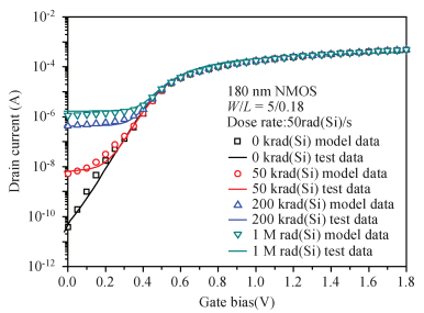
Table 1. Analytical model parameters.

|
| [1] |
Barnaby H J. Total-ionizing-dose effects in modern CMOS technologies. IEEE Trans Nucl Sci, 2006, 53(6): 3103 doi: 10.1109/TNS.2006.885952
|
| [2] |
McLain M L, Barnaby H J, Holbert K E, et al. Enhanced TID susceptibility in sub-100-nm bulk CMOS I/Otransistors and circuits. IEEE Trans Nucl Sci, 2007, 54(6): 2210 doi: 10.1109/TNS.2007.908461
|
| [3] |
Faccio F, Cervelli G. Radiation-induced edge effects in deep submicron CMOS transistors. IEEE Trans Nucl Sci, 2007, 52(6): 2413 https://www.researchgate.net/publication/3139618_Radiation-induced_edge_effects_in_deep_submicron_CMOS_transistors
|
| [4] |
Ding Lili, Guo Hongxia, Chen Wei, et al. Study of radiation induced leakage current between adjacent devices in a CMOS integrated circuit. Journal of Semiconductors, 2012, 33(6): 064006 doi: 10.1088/1674-4926/33/6/064006
|
| [5] |
Zhao Yuanfu, Zheng Hongchao, Fan Long, et al. Experimental research on transient radiation effects in microprocessors based on SPARC-V8 architecture. Journal of Semiconductors, 2015, 36(11): 114008 doi: 10.1088/1674-4926/36/11/114008
|
| [6] |
Li Leilei, Zhou Xinjie, Yu Zongguang, et al. Effect of phosphorus ion implantation on back gate effect of partially depleted SOI NMOS under total dose radiation. Journal of Semiconductors, 2015, 36(1): 014006 doi: 10.1088/1674-4926/36/1/014006
|
| [7] |
Peng C, Hu Z Y, Zhang Z X, et al. A new method for extracting the radiation induced trapped charge density along the STI sidewall in the PDSOI NMOSFETs. IEEE Trans Nucl Sci, 2013, 60(6): 4697 doi: 10.1109/TNS.2013.2283504
|
| [8] |
H Z Y, Liu Z L, Shao H, et al. Comprehensive study on the total dose effects in a 180-nm CMOS technology. IEEE Trans Nucl Sci, 2011, 58 (3): 1347 doi: 10.1109/TNS.2011.2132145
|
| [9] |
Fleetwood D M. Total ionizing dose effects in MOS and low dose-rate-sensitive linear-bipolar. IEEE Trans Nucl Sci, 2013, 60(3): 1706 doi: 10.1109/TNS.2013.2259260
|
| [10] |
Turowski M, Raman A, Schrimpf R D. Nonuniform total-dose-induced charge distribution in shallow-trench isolation oxides. IEEE Trans Nucl Sci, 2004, 51(6): 3166 doi: 10.1109/TNS.2004.839201
|
| [11] |
Johnston A H, Swimm R T, Allen G R, et al. Total dose effects in CMOS trench isolation regions. IEEE Trans Nucl Sci, 2009, 56(4): 1941 doi: 10.1109/TNS.2009.2019273
|
| [12] |
Esqueda I S, Barnaby H J. Modeling the non-uniform distribution of radiation-induced interface traps. IEEE Trans Nucl Sci, 2012, 59(4): 723 doi: 10.1109/TNS.2012.2186826
|
| [13] |
Tang Zhaohuan, Liu Rongkan, Tan Kaizhou, et al. A novel terminal structure for total dose irradiation hardened of a P-VDMOS. Journal of Semiconductors, 2014, 35(5): 054005 doi: 10.1088/1674-4926/35/5/054005
|
| [14] |
McLean F B. A framework for understanding radiation-induced interface states in SiO2 MOS structures. IEEE Trans Nucl Sci, 1980, 27(6): 1651 doi: 10.1109/TNS.1980.4331084
|
| [15] |
Shaneyfelt M R, Schwank J R, Fleetwood D M, et al. Field dependence of interface-trap buildup in polysilicon and metal gate MOS devices. IEEE Trans Nucl Sci, 1990, 37(6): 1632 doi: 10.1109/23.101171
|
| [16] |
Zhao Qifeng, Zhuang Yiqi, Bao Junlin, et al. Model of radiation induced gain degradation of NPN junction transistor at different dose rates. Journal of Semiconductors, 2015, 36(6): 064007 doi: 10.1088/1674-4926/36/6/064007
|
| [17] |
Zebrev G I, Petrov A S, Useinov R G, et al. Simulation of bipolar transistor degradation at various dose rates and electrical modes for high dose conditions. IEEE Trans Nucl Sci, 2014, 61(4): 1785 doi: 10.1109/TNS.2014.2315672
|
| [18] |
Barnaby H J, McLain M L, Esqueda I S, et al. Modeling ionizing radiation effects in solid state materials and CMOS devices. IEEE Trans Circuits Syst I, 2009, 56(6): 1870 http://cn.bing.com/academic/profile?id=1993083796&encoded=0&v=paper_preview&mkt=zh-cn
|
| [19] |
Chen X J, Barnaby H J, Adell P, et al. Modeling the dose rate response and the effects of hydrogen in bipolar technologies. IEEE Trans Nucl Sci, 2009, 56(6): 3196 doi: 10.1109/TNS.2009.2034154
|
| [20] |
Rashkeev S N, Fleetwood D M, Schrimpf R D, et al. Effects of hydrogen motion on interface trap formation and annealing. IEEE Trans Nucl Sci, 2004, 51(6): 3158 doi: 10.1109/TNS.2004.839202
|
| [21] |
Hughart D R, Schrimpf R D, Fleetwood D M, et al. The effects of proton defect interactions on radiation induced interface-trap formation and annealing. IEEE Trans Nucl Sci, 2012, 59(6): 3087 doi: 10.1109/TNS.2012.2220982
|
| [22] |
Wu W, Chen T, Gildenblat G, et al. Physics-based mathematical conditioning of the MOSFET surface potential equation. IEEE Trans Electron Devices, 2004, 51(6): 1196 https://www.researchgate.net/publication/3065305_Physics-Based_Mathematical_Conditioning_of_the_MOSFET_Surface_Potential_Equation
|
| [23] |
Brews J R. A charge-sheet model of the MOSFET. Solid-State Electron, 1978, 21: 345 doi: 10.1016/0038-1101(78)90264-2
|
| [24] |
Esqueda I S, Barnaby H J, Holbert K E. Modeling inter-device leakage in 90 nm bulk CMOS devices. IEEE Trans Nucl Sci, 2011, 58(3): 793 doi: 10.1109/TNS.2010.2101616
|
| [25] |
Hjalmarson H P, Pease R L, Devine R A B. Calculations of radiation dose-rate sensitivity of bipolar transistors. IEEE Trans Nucl Sci, 2008, 55(6): 3009 doi: 10.1109/TNS.2008.2007487
|
| [26] |
Johnston A H, Swimm R T, Miyahira T F. Low dose rate effects in shallow trench isolation regions. IEEE Trans Nucl Sci, 2010, 57(6): 3279 https://www.researchgate.net/publication/224202890_Low_Dose_Rate_Effects_in_Shallow_Trench_Isolation_Regions
|
| [27] |
Liu Z L, Hu Z Y, Shao H, et al. Total ionizing dose effects of elementary devices for control circuit of 0.18 μ m flash technology. IEEE Nuclear and Space Radiation Effects Conference (NSREC), Las Vegas, USA, 2011
|


Article views: 4399 Times PDF downloads: 166 Times Cited by: 0 Times
Received: 30 March 2016 Revised: 12 May 2016 Online: Published: 01 December 2016
| Citation: |
Baoping He, Zujun Wang, Jiangkun Sheng, Shaoyan Huang. Total ionizing dose radiation effects on NMOS parasitic transistors in advanced bulk CMOS technology devices[J]. Journal of Semiconductors, 2016, 37(12): 124003. doi: 10.1088/1674-4926/37/12/124003
****
B P He, Z J Wang, J K Sheng, S Y Huang. Total ionizing dose radiation effects on NMOS parasitic transistors in advanced bulk CMOS technology devices[J]. J. Semicond., 2016, 37(12): 124003. doi: 10.1088/1674-4926/37/12/124003.

|
| [1] |
Barnaby H J. Total-ionizing-dose effects in modern CMOS technologies. IEEE Trans Nucl Sci, 2006, 53(6): 3103 doi: 10.1109/TNS.2006.885952
|
| [2] |
McLain M L, Barnaby H J, Holbert K E, et al. Enhanced TID susceptibility in sub-100-nm bulk CMOS I/Otransistors and circuits. IEEE Trans Nucl Sci, 2007, 54(6): 2210 doi: 10.1109/TNS.2007.908461
|
| [3] |
Faccio F, Cervelli G. Radiation-induced edge effects in deep submicron CMOS transistors. IEEE Trans Nucl Sci, 2007, 52(6): 2413 https://www.researchgate.net/publication/3139618_Radiation-induced_edge_effects_in_deep_submicron_CMOS_transistors
|
| [4] |
Ding Lili, Guo Hongxia, Chen Wei, et al. Study of radiation induced leakage current between adjacent devices in a CMOS integrated circuit. Journal of Semiconductors, 2012, 33(6): 064006 doi: 10.1088/1674-4926/33/6/064006
|
| [5] |
Zhao Yuanfu, Zheng Hongchao, Fan Long, et al. Experimental research on transient radiation effects in microprocessors based on SPARC-V8 architecture. Journal of Semiconductors, 2015, 36(11): 114008 doi: 10.1088/1674-4926/36/11/114008
|
| [6] |
Li Leilei, Zhou Xinjie, Yu Zongguang, et al. Effect of phosphorus ion implantation on back gate effect of partially depleted SOI NMOS under total dose radiation. Journal of Semiconductors, 2015, 36(1): 014006 doi: 10.1088/1674-4926/36/1/014006
|
| [7] |
Peng C, Hu Z Y, Zhang Z X, et al. A new method for extracting the radiation induced trapped charge density along the STI sidewall in the PDSOI NMOSFETs. IEEE Trans Nucl Sci, 2013, 60(6): 4697 doi: 10.1109/TNS.2013.2283504
|
| [8] |
H Z Y, Liu Z L, Shao H, et al. Comprehensive study on the total dose effects in a 180-nm CMOS technology. IEEE Trans Nucl Sci, 2011, 58 (3): 1347 doi: 10.1109/TNS.2011.2132145
|
| [9] |
Fleetwood D M. Total ionizing dose effects in MOS and low dose-rate-sensitive linear-bipolar. IEEE Trans Nucl Sci, 2013, 60(3): 1706 doi: 10.1109/TNS.2013.2259260
|
| [10] |
Turowski M, Raman A, Schrimpf R D. Nonuniform total-dose-induced charge distribution in shallow-trench isolation oxides. IEEE Trans Nucl Sci, 2004, 51(6): 3166 doi: 10.1109/TNS.2004.839201
|
| [11] |
Johnston A H, Swimm R T, Allen G R, et al. Total dose effects in CMOS trench isolation regions. IEEE Trans Nucl Sci, 2009, 56(4): 1941 doi: 10.1109/TNS.2009.2019273
|
| [12] |
Esqueda I S, Barnaby H J. Modeling the non-uniform distribution of radiation-induced interface traps. IEEE Trans Nucl Sci, 2012, 59(4): 723 doi: 10.1109/TNS.2012.2186826
|
| [13] |
Tang Zhaohuan, Liu Rongkan, Tan Kaizhou, et al. A novel terminal structure for total dose irradiation hardened of a P-VDMOS. Journal of Semiconductors, 2014, 35(5): 054005 doi: 10.1088/1674-4926/35/5/054005
|
| [14] |
McLean F B. A framework for understanding radiation-induced interface states in SiO2 MOS structures. IEEE Trans Nucl Sci, 1980, 27(6): 1651 doi: 10.1109/TNS.1980.4331084
|
| [15] |
Shaneyfelt M R, Schwank J R, Fleetwood D M, et al. Field dependence of interface-trap buildup in polysilicon and metal gate MOS devices. IEEE Trans Nucl Sci, 1990, 37(6): 1632 doi: 10.1109/23.101171
|
| [16] |
Zhao Qifeng, Zhuang Yiqi, Bao Junlin, et al. Model of radiation induced gain degradation of NPN junction transistor at different dose rates. Journal of Semiconductors, 2015, 36(6): 064007 doi: 10.1088/1674-4926/36/6/064007
|
| [17] |
Zebrev G I, Petrov A S, Useinov R G, et al. Simulation of bipolar transistor degradation at various dose rates and electrical modes for high dose conditions. IEEE Trans Nucl Sci, 2014, 61(4): 1785 doi: 10.1109/TNS.2014.2315672
|
| [18] |
Barnaby H J, McLain M L, Esqueda I S, et al. Modeling ionizing radiation effects in solid state materials and CMOS devices. IEEE Trans Circuits Syst I, 2009, 56(6): 1870 http://cn.bing.com/academic/profile?id=1993083796&encoded=0&v=paper_preview&mkt=zh-cn
|
| [19] |
Chen X J, Barnaby H J, Adell P, et al. Modeling the dose rate response and the effects of hydrogen in bipolar technologies. IEEE Trans Nucl Sci, 2009, 56(6): 3196 doi: 10.1109/TNS.2009.2034154
|
| [20] |
Rashkeev S N, Fleetwood D M, Schrimpf R D, et al. Effects of hydrogen motion on interface trap formation and annealing. IEEE Trans Nucl Sci, 2004, 51(6): 3158 doi: 10.1109/TNS.2004.839202
|
| [21] |
Hughart D R, Schrimpf R D, Fleetwood D M, et al. The effects of proton defect interactions on radiation induced interface-trap formation and annealing. IEEE Trans Nucl Sci, 2012, 59(6): 3087 doi: 10.1109/TNS.2012.2220982
|
| [22] |
Wu W, Chen T, Gildenblat G, et al. Physics-based mathematical conditioning of the MOSFET surface potential equation. IEEE Trans Electron Devices, 2004, 51(6): 1196 https://www.researchgate.net/publication/3065305_Physics-Based_Mathematical_Conditioning_of_the_MOSFET_Surface_Potential_Equation
|
| [23] |
Brews J R. A charge-sheet model of the MOSFET. Solid-State Electron, 1978, 21: 345 doi: 10.1016/0038-1101(78)90264-2
|
| [24] |
Esqueda I S, Barnaby H J, Holbert K E. Modeling inter-device leakage in 90 nm bulk CMOS devices. IEEE Trans Nucl Sci, 2011, 58(3): 793 doi: 10.1109/TNS.2010.2101616
|
| [25] |
Hjalmarson H P, Pease R L, Devine R A B. Calculations of radiation dose-rate sensitivity of bipolar transistors. IEEE Trans Nucl Sci, 2008, 55(6): 3009 doi: 10.1109/TNS.2008.2007487
|
| [26] |
Johnston A H, Swimm R T, Miyahira T F. Low dose rate effects in shallow trench isolation regions. IEEE Trans Nucl Sci, 2010, 57(6): 3279 https://www.researchgate.net/publication/224202890_Low_Dose_Rate_Effects_in_Shallow_Trench_Isolation_Regions
|
| [27] |
Liu Z L, Hu Z Y, Shao H, et al. Total ionizing dose effects of elementary devices for control circuit of 0.18 μ m flash technology. IEEE Nuclear and Space Radiation Effects Conference (NSREC), Las Vegas, USA, 2011
|

 WeChat ID
Journal of Semiconductors © 2017 All Rights Reserved 京ICP备05085259号-2

 DownLoad: