


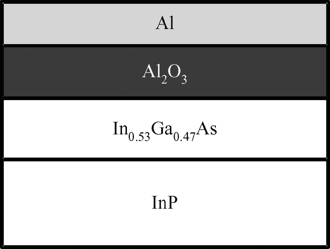
Fig. 1.
Schematic diagram of fabricated In0:53Ga0:47As MOS capacitor.
SEMICONDUCTOR TECHNOLOGY
Zizeng Lin1, 2, Mingmin Cao1, 2, Shengkai Wang2, Qi Li1, Gongli Xiao1, Xi Gao1, Honggang Liu2 and Haiou Li1,
Corresponding author: Haiou Li, seagull_1228@163.com
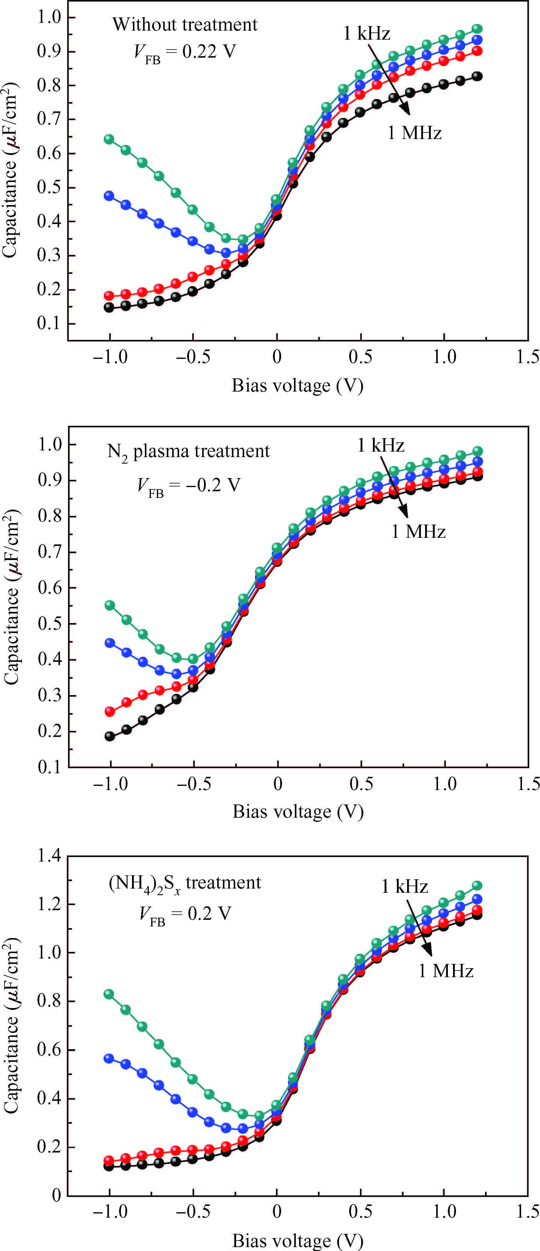
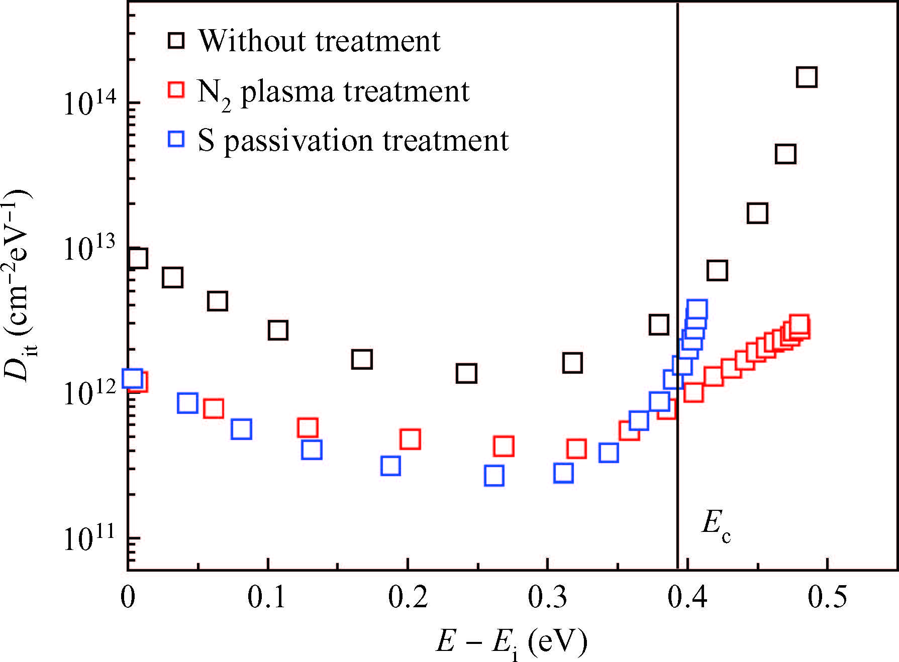
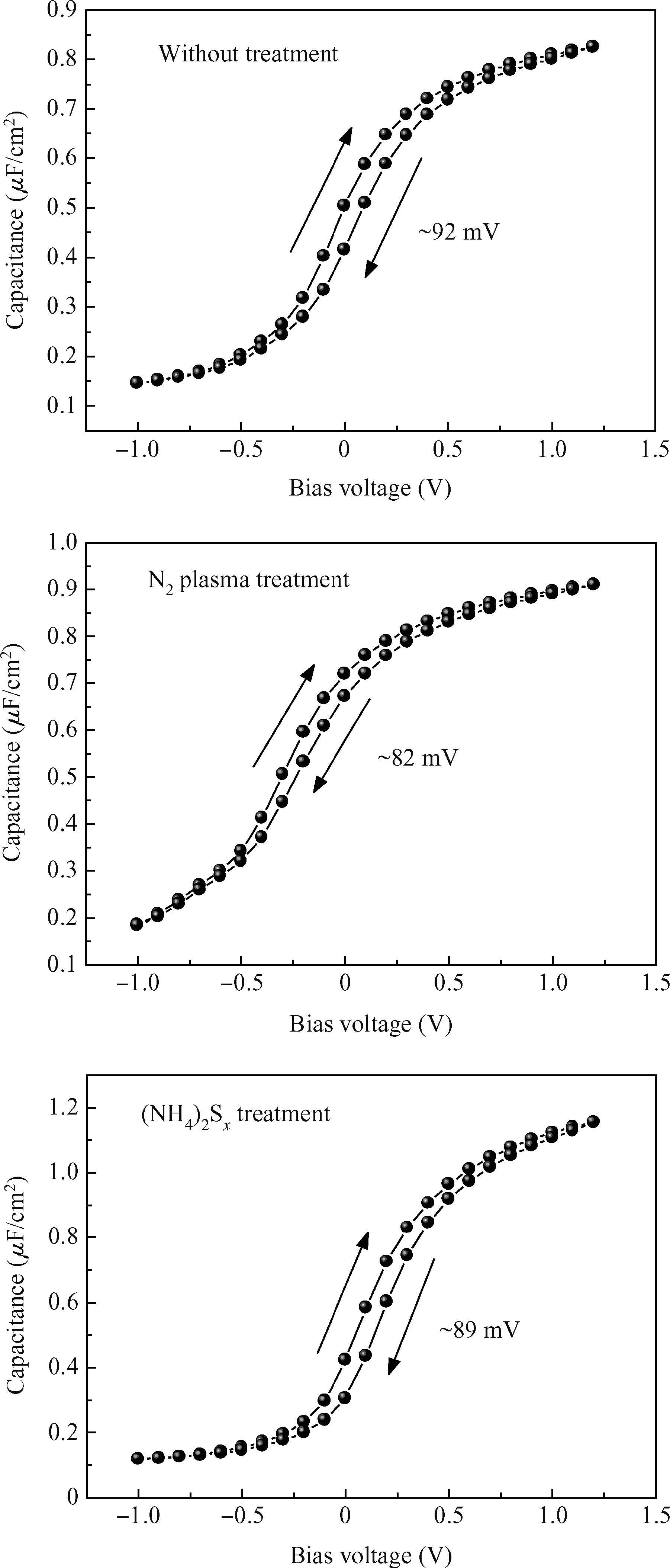
Abstract: The impact of nitridation and sulfur passivation for In0.53Ga0.47As surfaces on the Al/Al2O3/InGaAs MOS capacitors properties was investigated by comparing the characteristics of frequency dispersion and hysteresis, calculating the Dit and Δ Nbt values, and analyzing the interface traps and the leakage current. The results showed that both of the methods could form a passivation-layer on the InGaAs surface. The samples treated by N2 plasma could obtain good interface properties with the smallest frequency dispersion in the accumulation region, and the best hysteresis characteristics and good I-V properties were presented. Also the samples with (NH4)2Sx treatment showed the smallest frequency dispersion near the flat-band region and a minimum Dit value of 2.6 × 1011 cm-2 eV-1.
Keywords: N2 plasma, (NH4)2Sx treatment, interface properties, MOS capacitors
| [1] | |
| [2] | |
| [3] | |
| [4] | |
| [5] | |
| [6] | |
| [7] | |
| [8] | |
| [9] | |
| [10] | |
| [11] | |
| [12] | |
| [13] | |
| [14] | |
| [15] | |
| [16] | |
| [17] | |
| [18] | |
| [19] |
| [1] | |
| [2] | |
| [3] | |
| [4] | |
| [5] | |
| [6] | |
| [7] | |
| [8] | |
| [9] | |
| [10] | |
| [11] | |
| [12] | |
| [13] | |
| [14] | |
| [15] | |
| [16] | |
| [17] | |
| [18] | |
| [19] |


Article views: 4005 Times PDF downloads: 28 Times Cited by: 0 Times
Received: 19 June 2015 Revised: Online: Published: 01 February 2016
| Citation: |
Zizeng Lin, Mingmin Cao, Shengkai Wang, Qi Li, Gongli Xiao, Xi Gao, Honggang Liu, Haiou Li. The effect of nitridation and sulfur passivation for In0.53Ga0.47As surfaces on their Al/Al2O3/InGaAs MOS capacitors properties[J]. Journal of Semiconductors, 2016, 37(2): 026002. doi: 10.1088/1674-4926/37/2/026002
****
Z Z Lin, M M Cao, S K Wang, Q Li, G L Xiao, X Gao, H G Liu, H O Li. The effect of nitridation and sulfur passivation for In0.53Ga0.47As surfaces on their Al/Al2O3/InGaAs MOS capacitors properties[J]. J. Semicond., 2016, 37(2): 026002. doi: 10.1088/1674-4926/37/2/026002.

|
| [1] | |
| [2] | |
| [3] | |
| [4] | |
| [5] | |
| [6] | |
| [7] | |
| [8] | |
| [9] | |
| [10] | |
| [11] | |
| [12] | |
| [13] | |
| [14] | |
| [15] | |
| [16] | |
| [17] | |
| [18] | |
| [19] |

 WeChat ID
Journal of Semiconductors © 2017 All Rights Reserved 京ICP备05085259号-2

 DownLoad:

