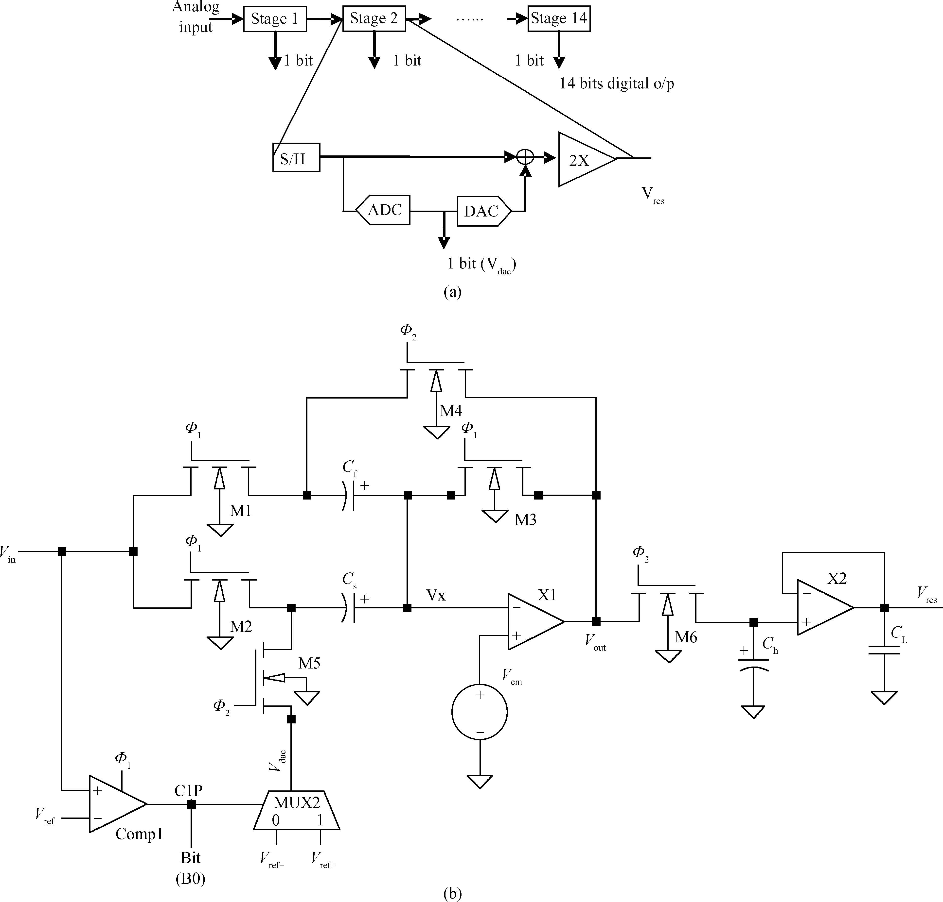
Fig. 1.
(a) 14-bit pipelined ADC with a single stage architecture. (b) Implementation of 1-bit pipelined ADC.
SEMICONDUCTOR INTEGRATED CIRCUITS
Swina Narula and Sujata Pandey
Corresponding author: Sujata Pandey, Email: spandey@amity.edu
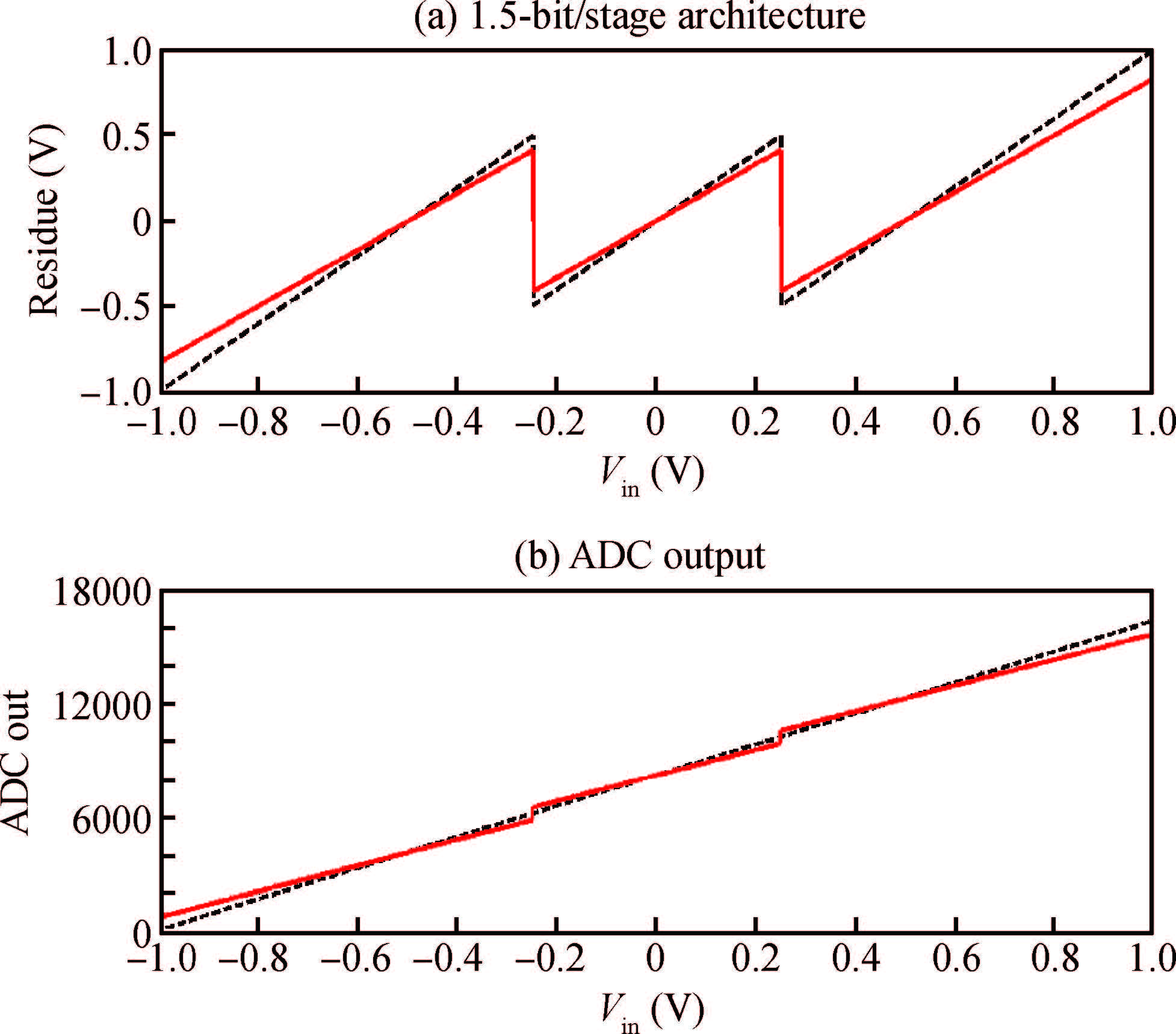
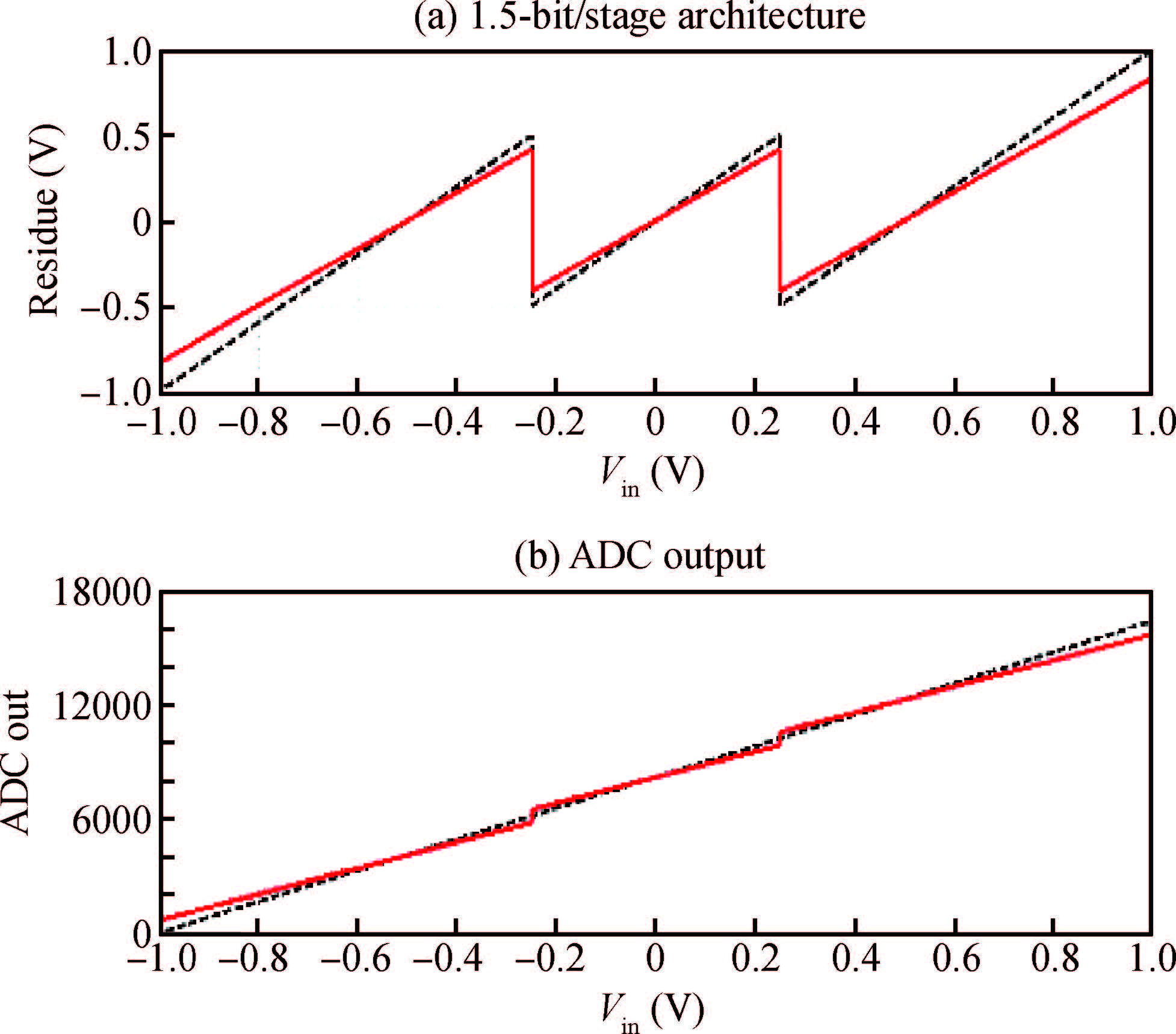
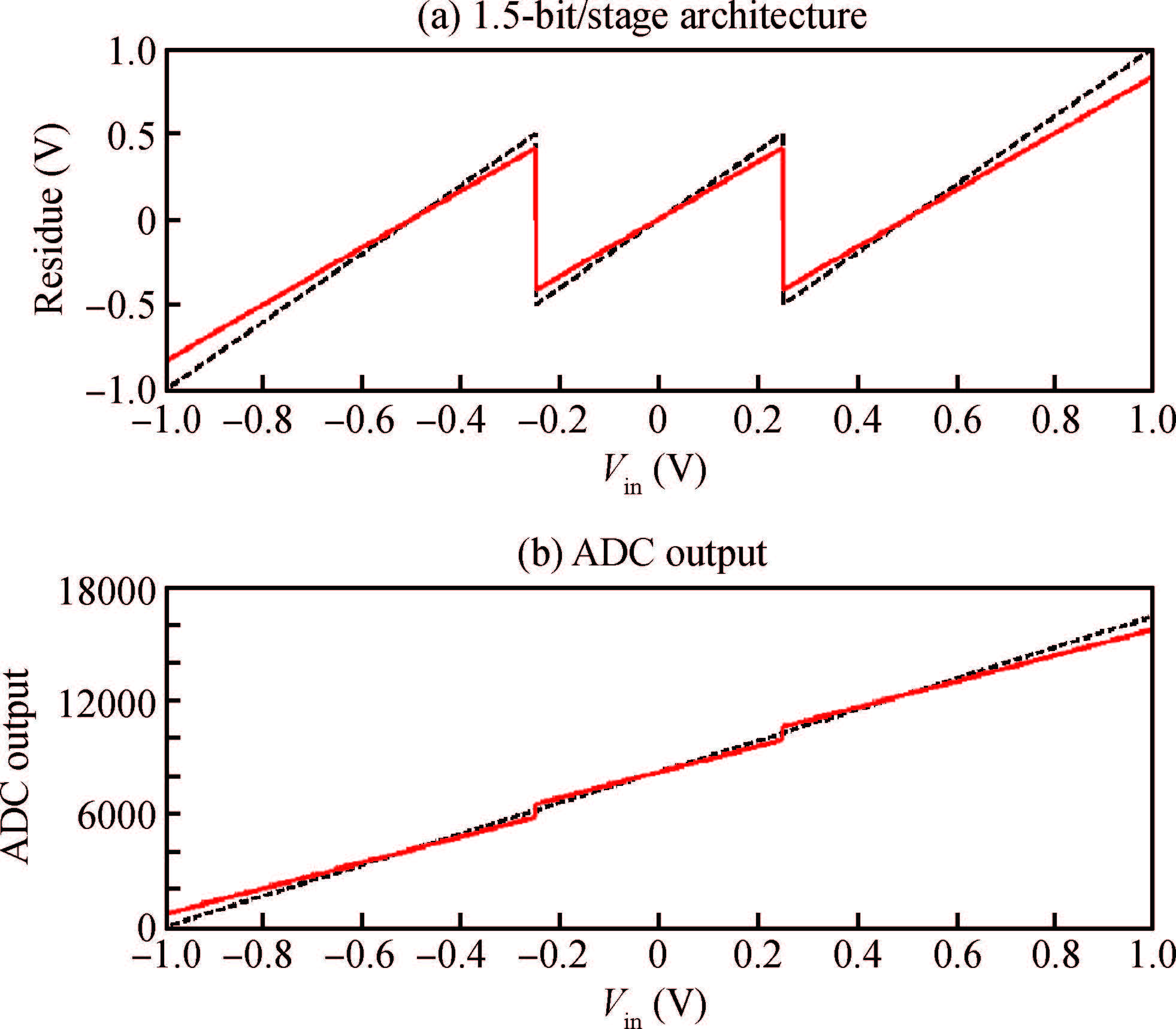
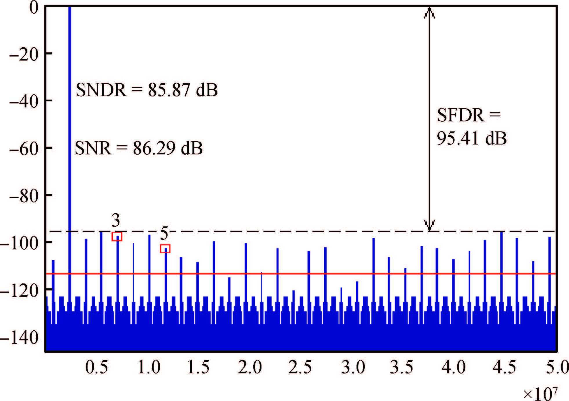
Abstract: A novel architecture of a pipelined redundant-signed-digit analog to digital converter(RSD-ADC) is presented featuring a high signal to noise ratio(SNR), spurious free dynamic range(SFDR) and signal to noise plus distortion(SNDR) with efficient background correction logic. The proposed ADC architecture shows high accuracy with a high speed circuit and efficient utilization of the hardware. This paper demonstrates the functionality of the digital correction logic of 14-bit pipelined ADC at each 1.5 bit/stage. This prototype of ADC architecture accounts for capacitor mismatch, comparator offset and finite Op-Amp gain error in the MDAC(residue amplification circuit) stages. With the proposed architecture of ADC, SNDR obtained is 85.89 dB, SNR is 85.9 dB and SFDR obtained is 102.8 dB at the sample rate of 100 MHz. This novel architecture of digital correction logic is transparent to the overall system, which is demonstrated by using 14-bit pipelined ADC. After a latency of 14 clocks, digital output will be available at every clock pulse. To describe the circuit behavior of the ADC, VHDL and MATLAB programs are used. The proposed architecture is also capable of reducing the digital hardware. Silicon area is also the complexity of the design.
Keywords: pipelined ADC, MDAC, non-ideal errors, signal to noise ratio(SNR), spurious free dynamic range(SFDR), signal to noise plus distortion(SNDR)
| [1] | |
| [2] | |
| [3] | |
| [4] | |
| [5] | |
| [6] | |
| [7] | |
| [8] | |
| [9] | |
| [10] | |
| [11] | |
| [12] | |
| [13] | |
| [14] | |
| [15] | |
| [16] | |
| [17] | |
| [18] | |
| [19] | |
| [20] | |
| [21] | |
| [22] | |
| [23] | |
| [24] | |
| [25] |
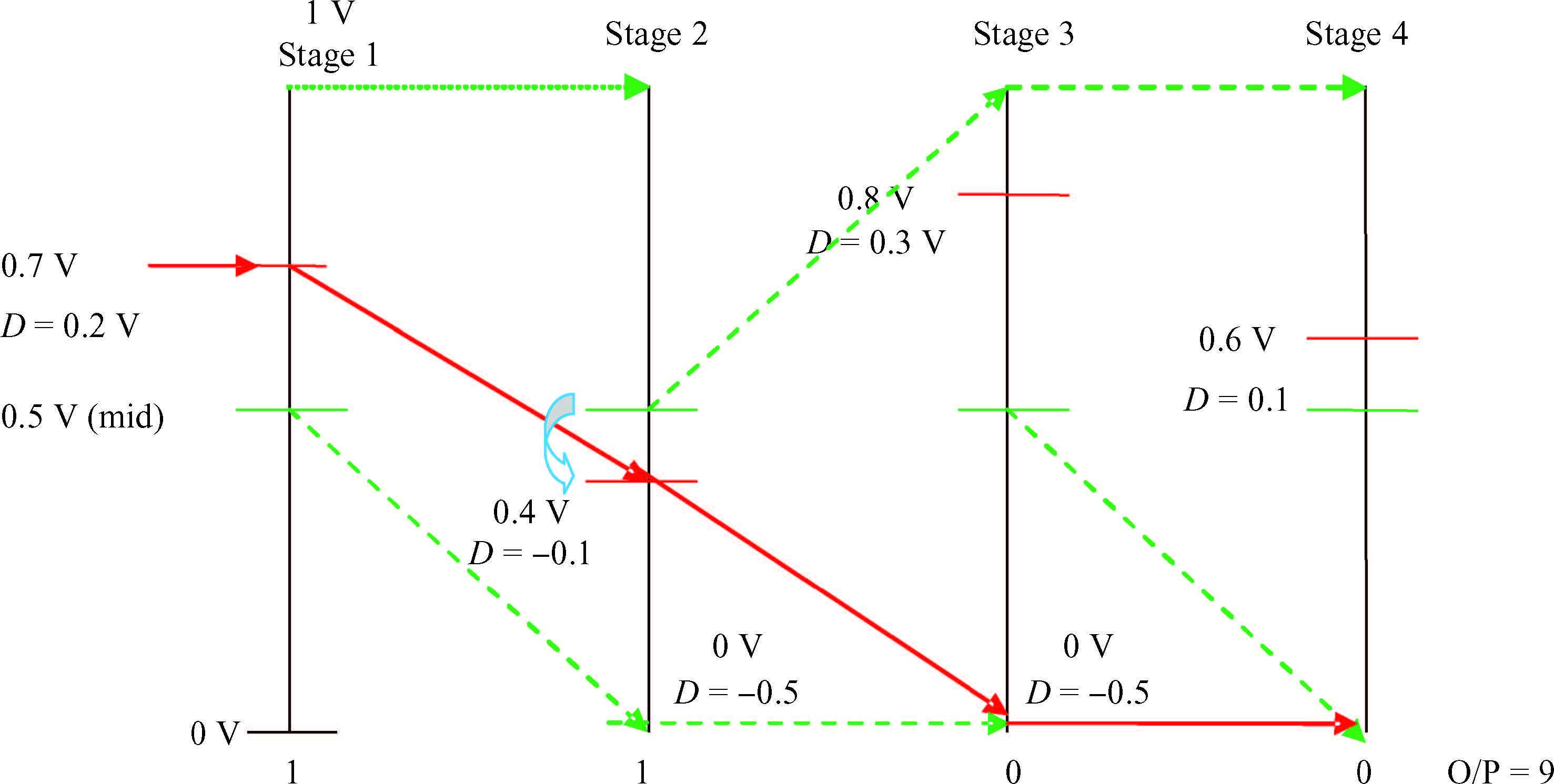
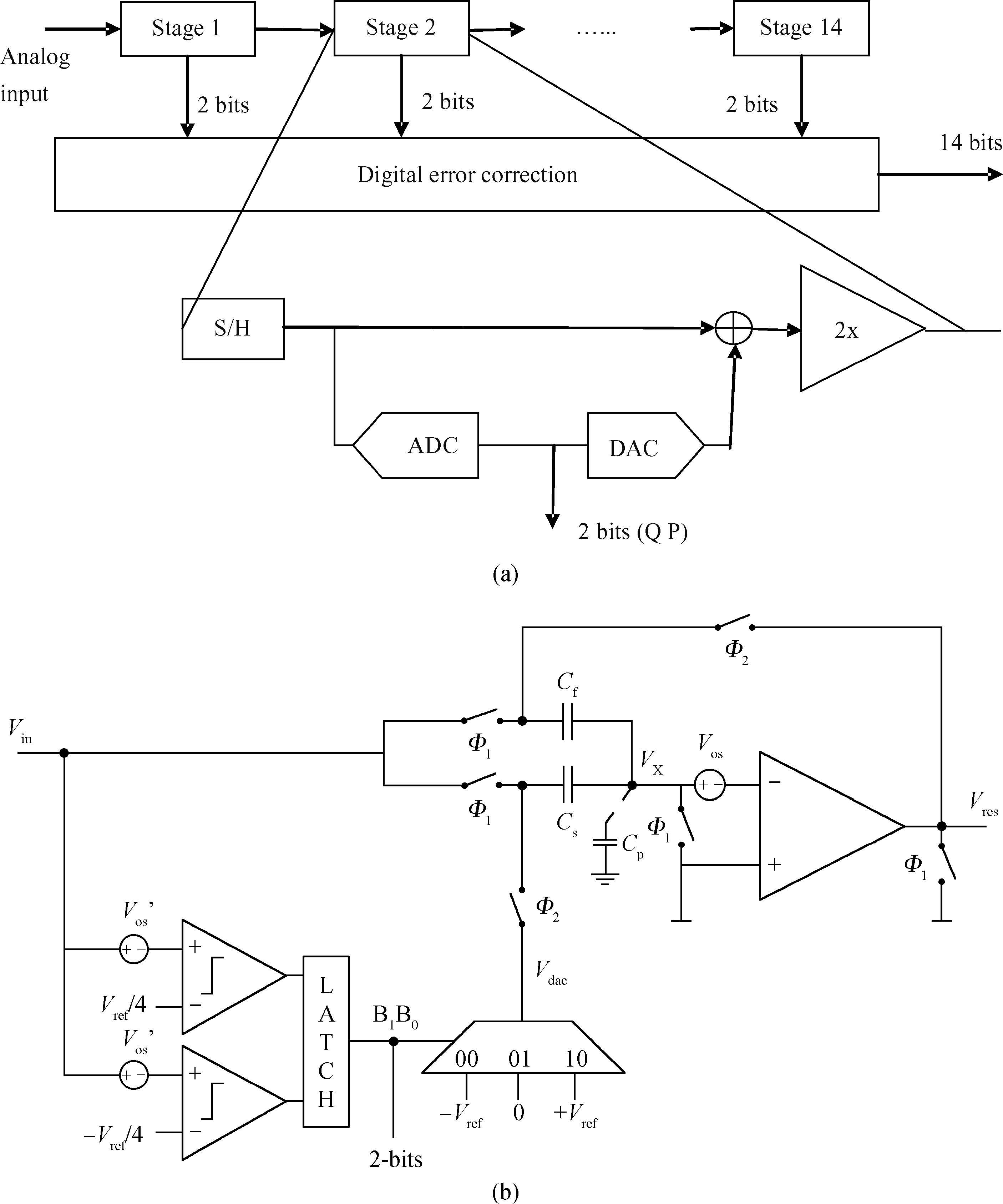
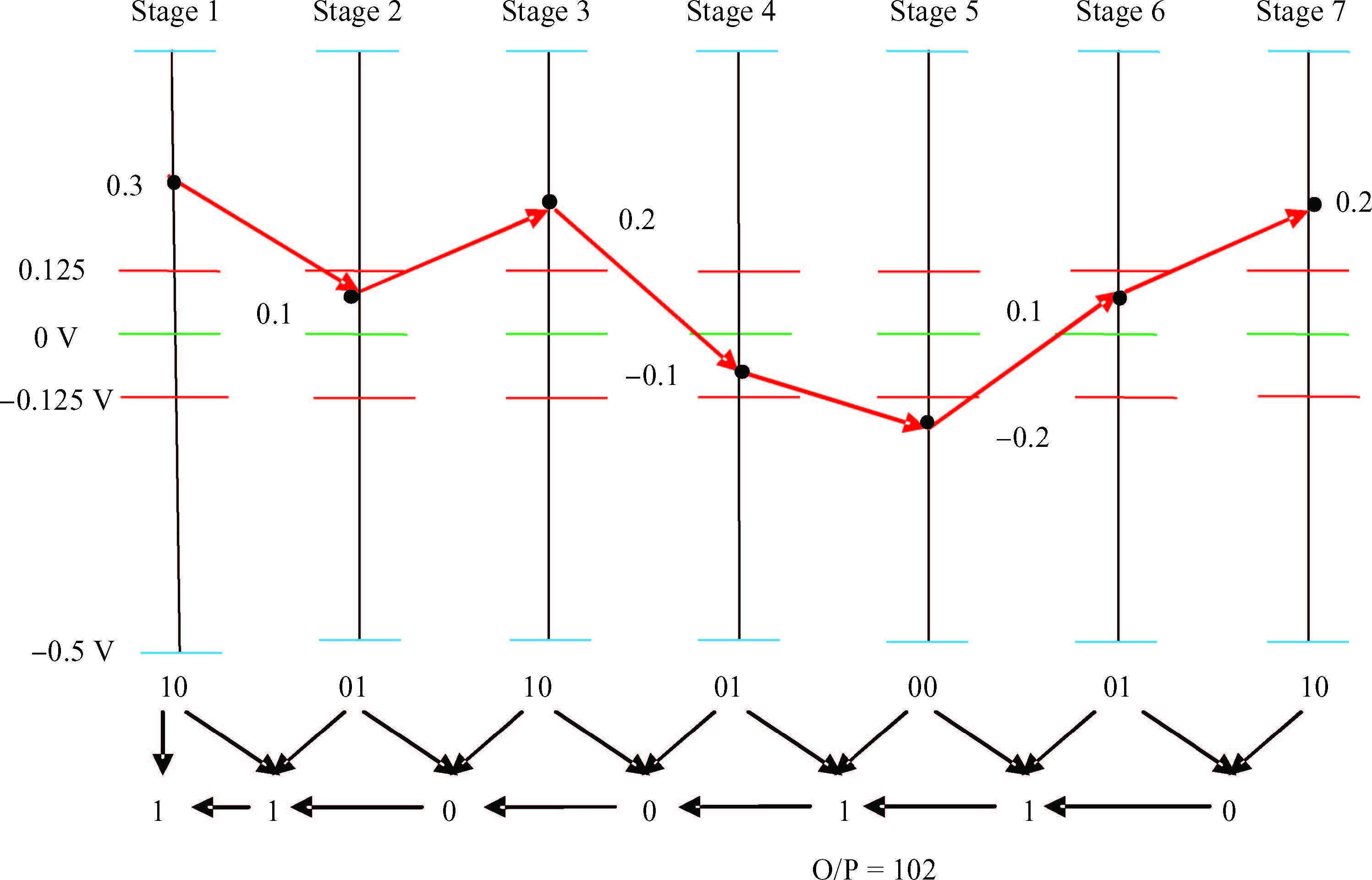
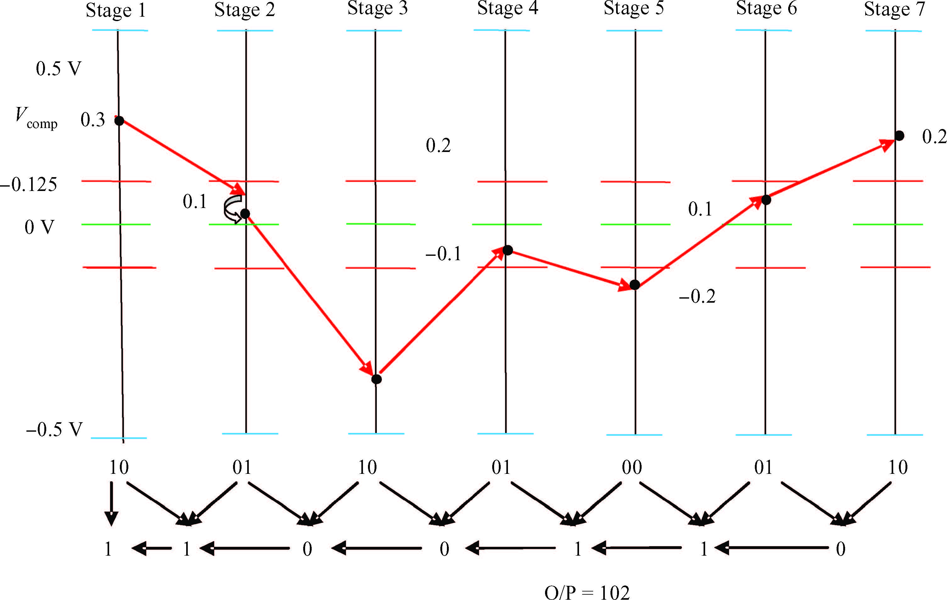
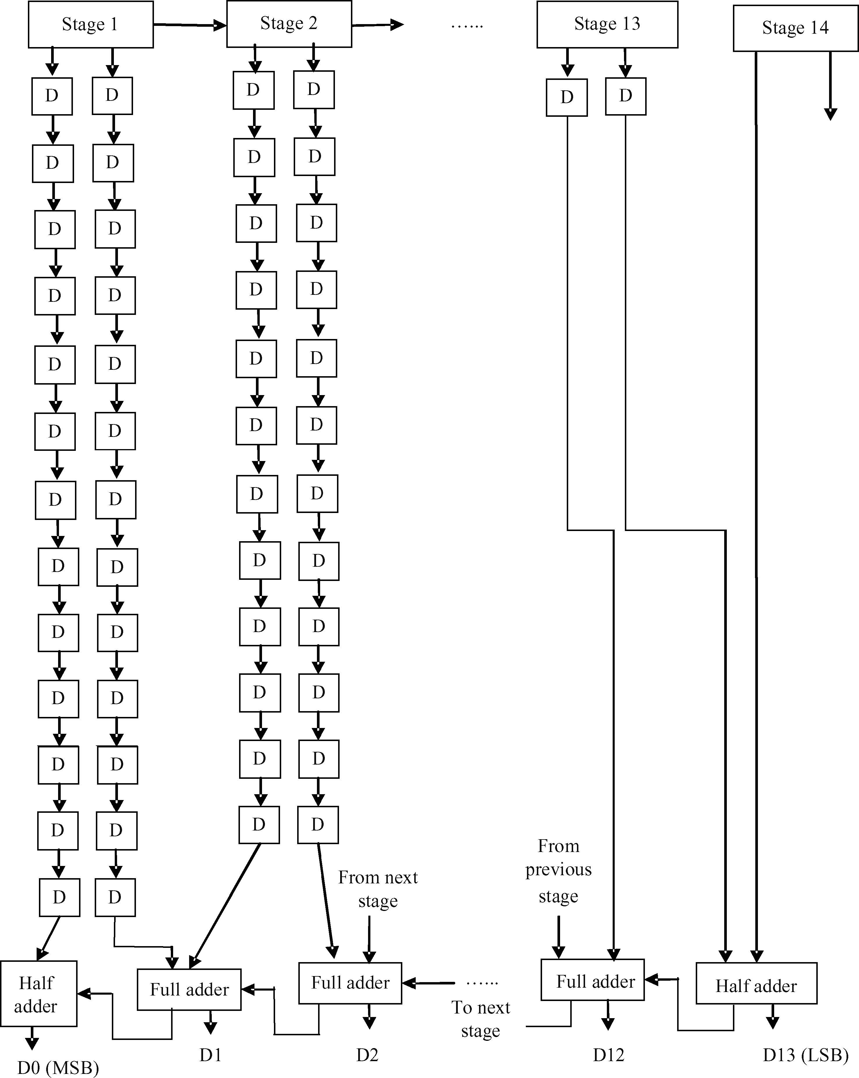
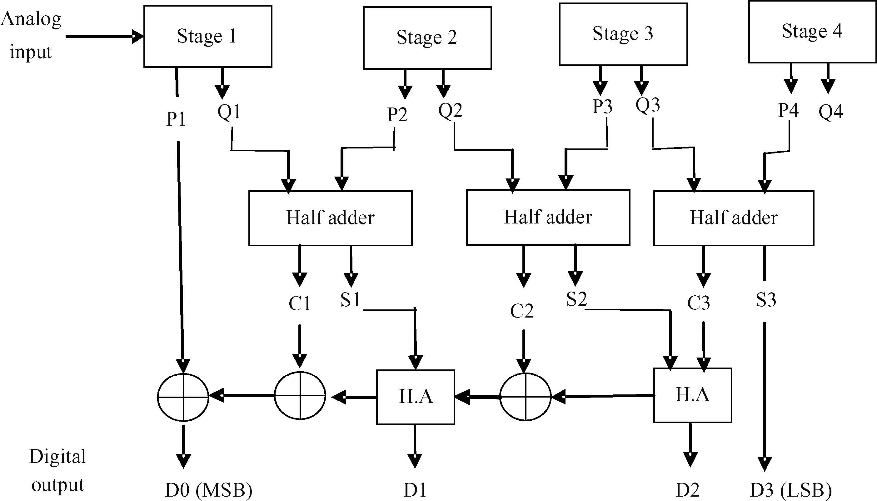
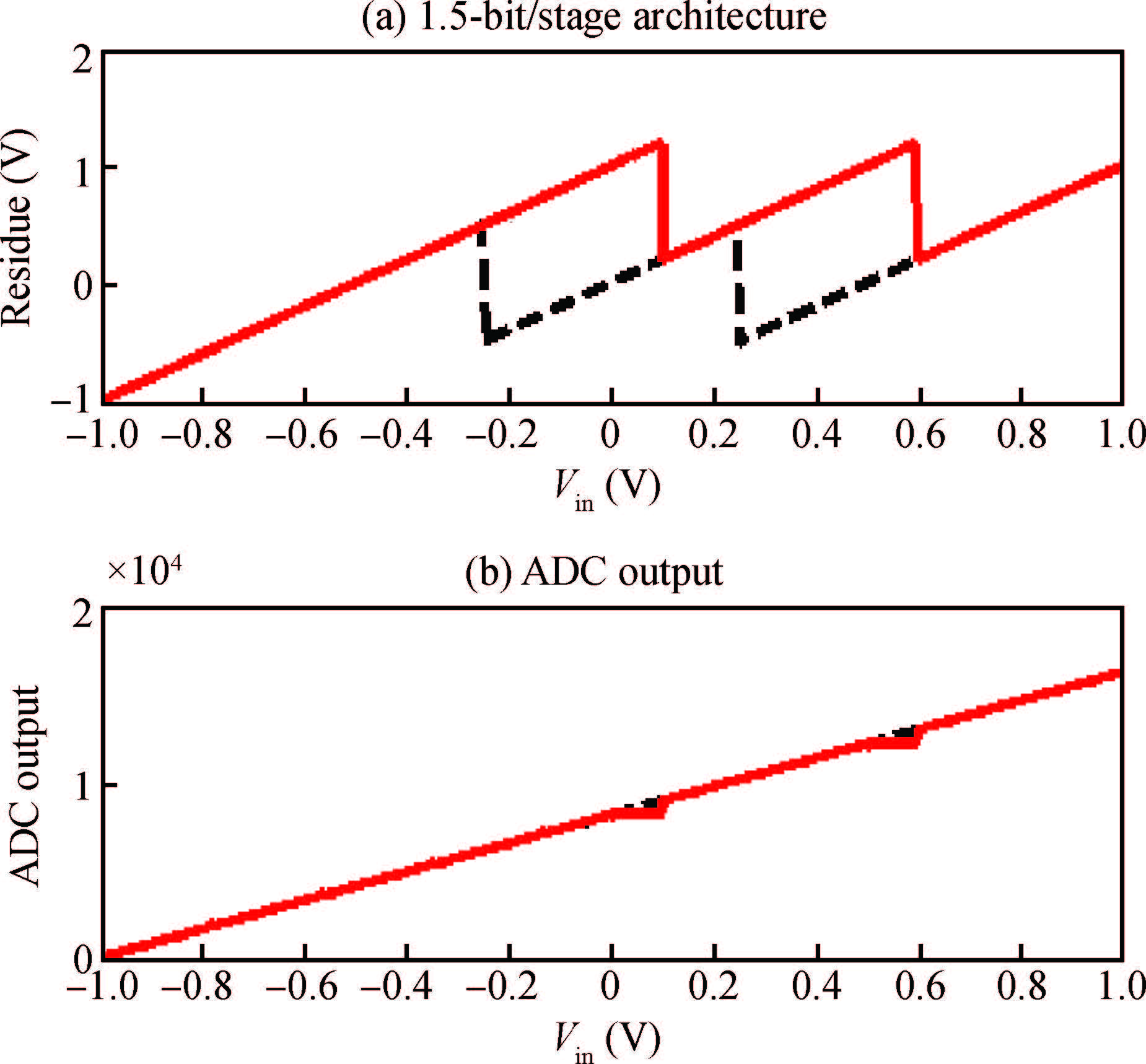
Table 1. Comparison of the performance of proposed model with other models of pipelined ADC.
 DownLoad: CSV
| [1] | |
| [2] | |
| [3] | |
| [4] | |
| [5] | |
| [6] | |
| [7] | |
| [8] | |
| [9] | |
| [10] | |
| [11] | |
| [12] | |
| [13] | |
| [14] | |
| [15] | |
| [16] | |
| [17] | |
| [18] | |
| [19] | |
| [20] | |
| [21] | |
| [22] | |
| [23] | |
| [24] | |
| [25] |


Article views: 4742 Times PDF downloads: 118 Times Cited by: 0 Times
Received: 12 July 2015 Revised: Online: Published: 01 March 2016
| Citation: |
Swina Narula, Sujata Pandey. High performance 14-bit pipelined redundant signed digit ADC[J]. Journal of Semiconductors, 2016, 37(3): 035001. doi: 10.1088/1674-4926/37/3/035001
****
S Narula, Sujata Pandey. High performance 14-bit pipelined redundant signed digit ADC[J]. J. Semicond., 2016, 37(3): 035001. doi: 10.1088/1674-4926/37/3/035001.

|
| [1] | |
| [2] | |
| [3] | |
| [4] | |
| [5] | |
| [6] | |
| [7] | |
| [8] | |
| [9] | |
| [10] | |
| [11] | |
| [12] | |
| [13] | |
| [14] | |
| [15] | |
| [16] | |
| [17] | |
| [18] | |
| [19] | |
| [20] | |
| [21] | |
| [22] | |
| [23] | |
| [24] | |
| [25] |

 WeChat ID
Journal of Semiconductors © 2017 All Rights Reserved 京ICP备05085259号-2