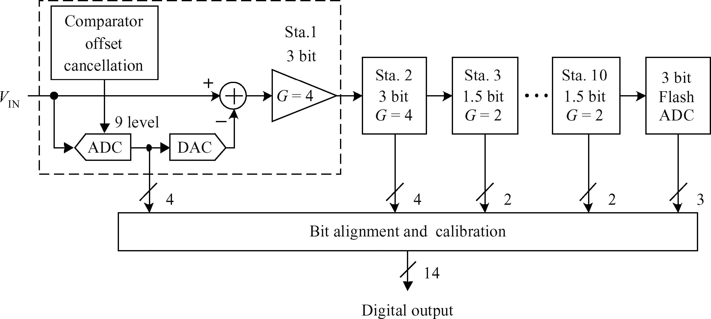
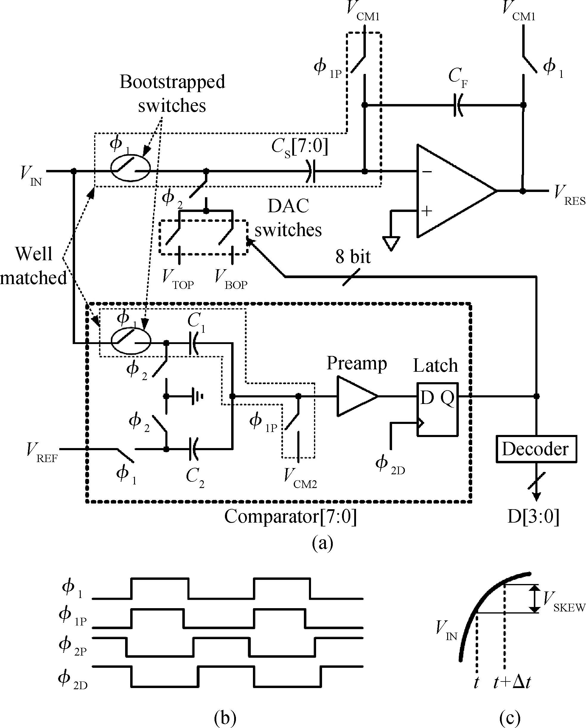
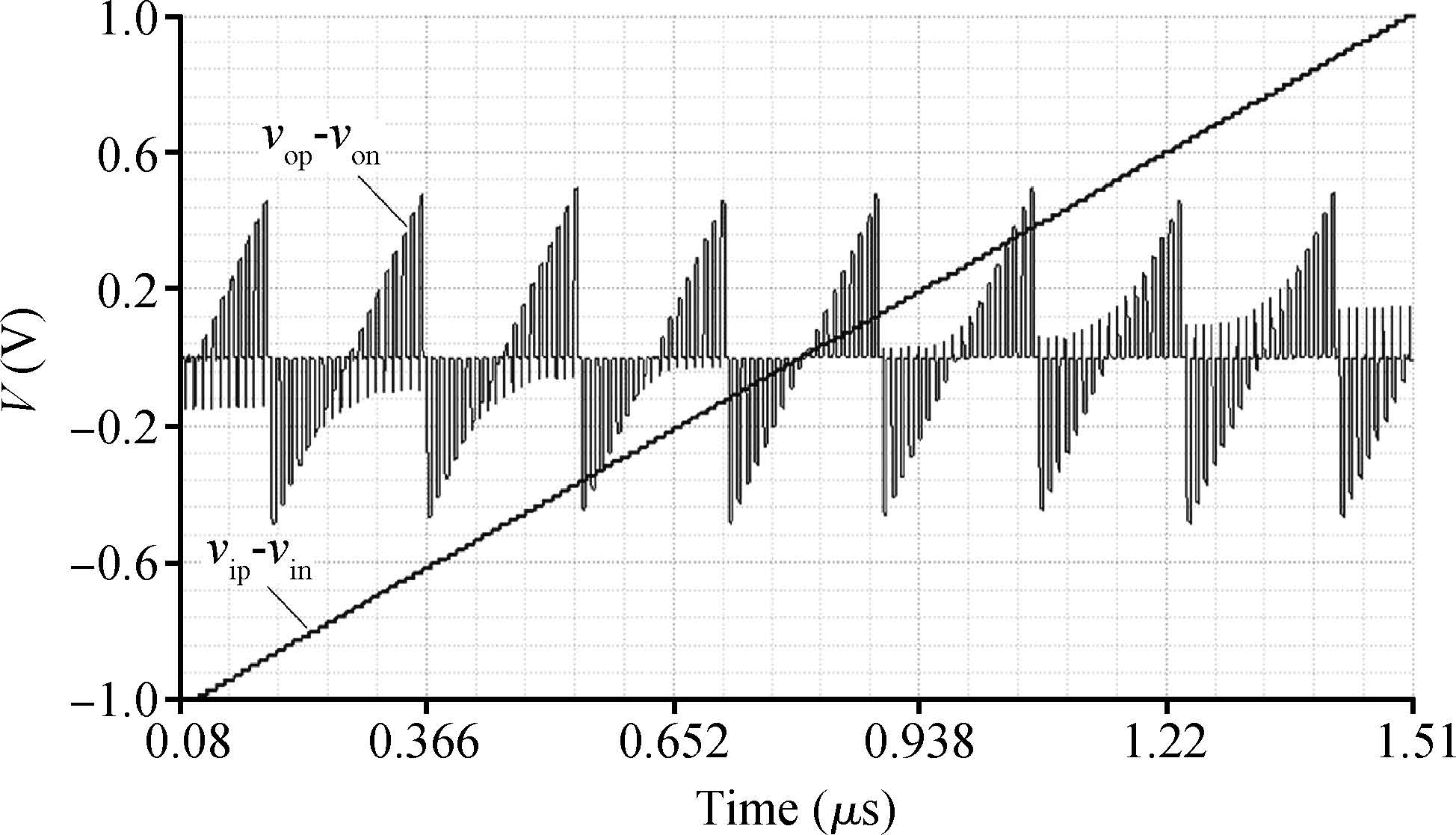
Fig1.
Architecture of the presented ADC.
SEMICONDUCTOR INTEGRATED CIRCUITS
Xiaofei Wang1, , Hong Zhang2, Jie Zhang2, Xin Du2 and Yue Hao1
Corresponding author: Wang Xiaofei, Email:xjtuwxf@126.com
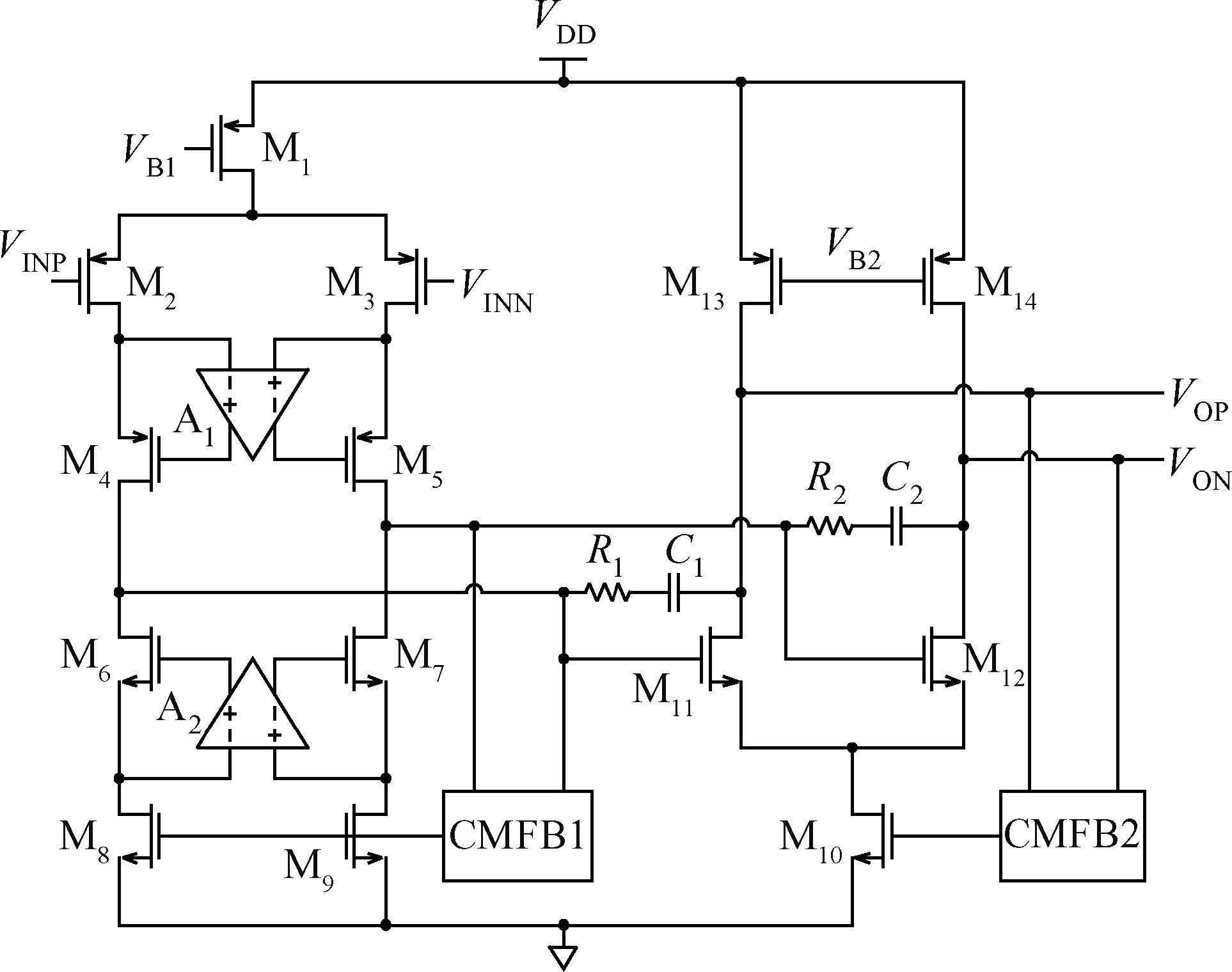
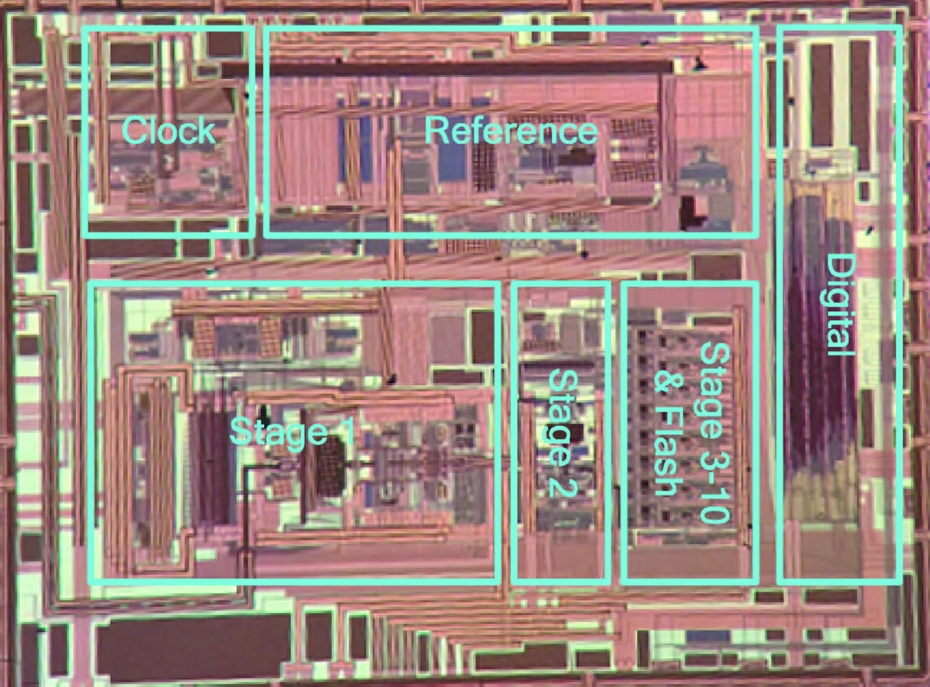
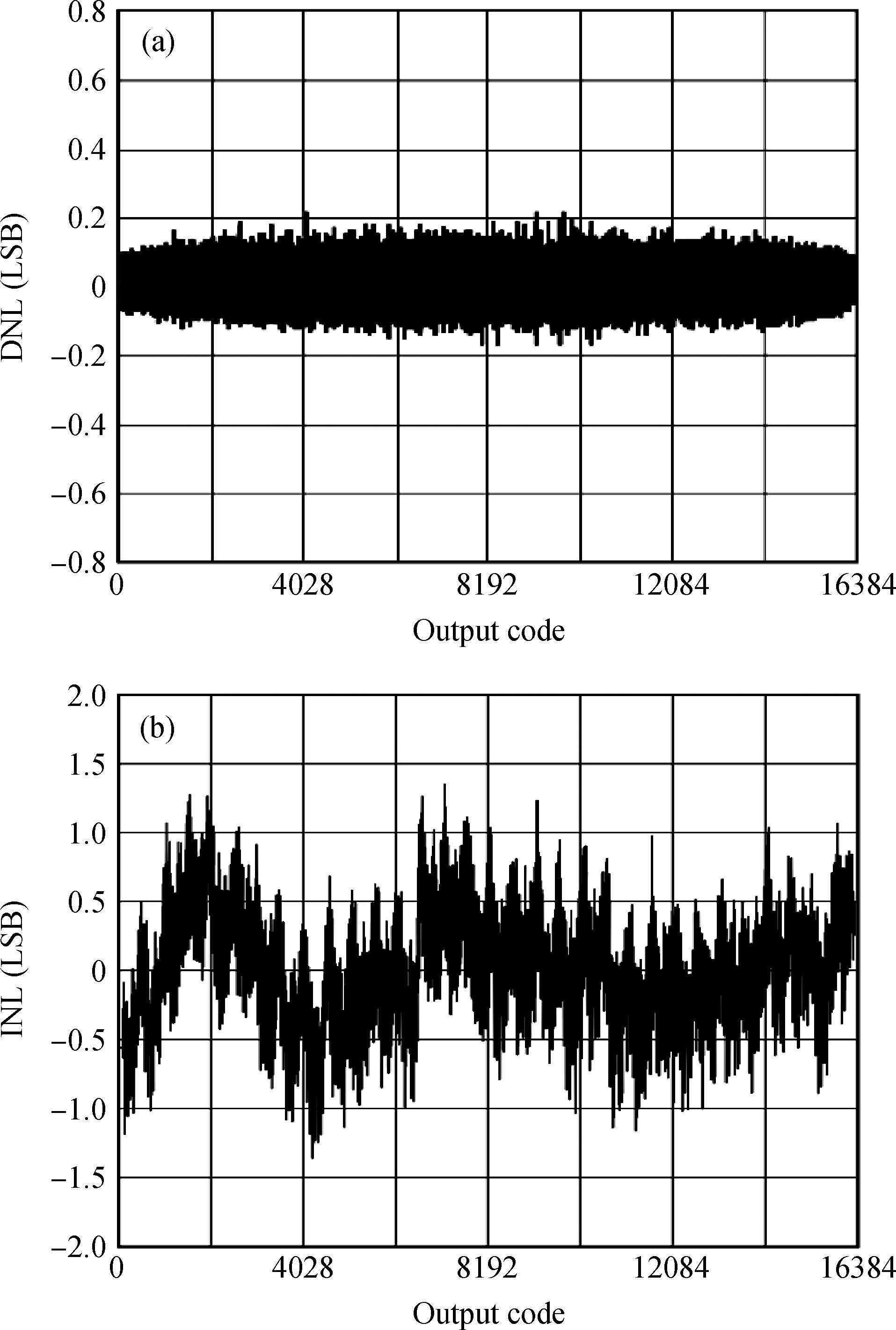
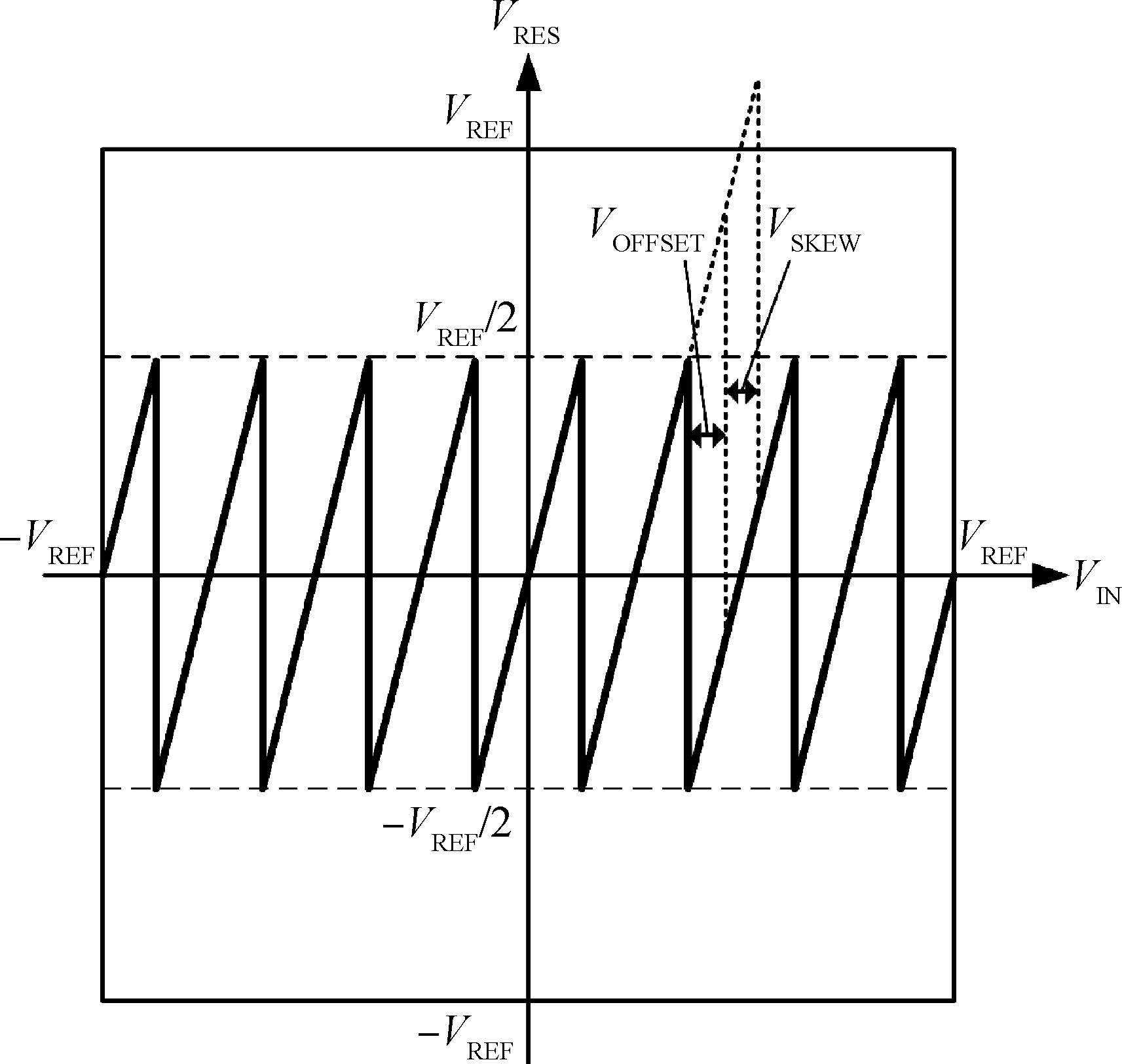
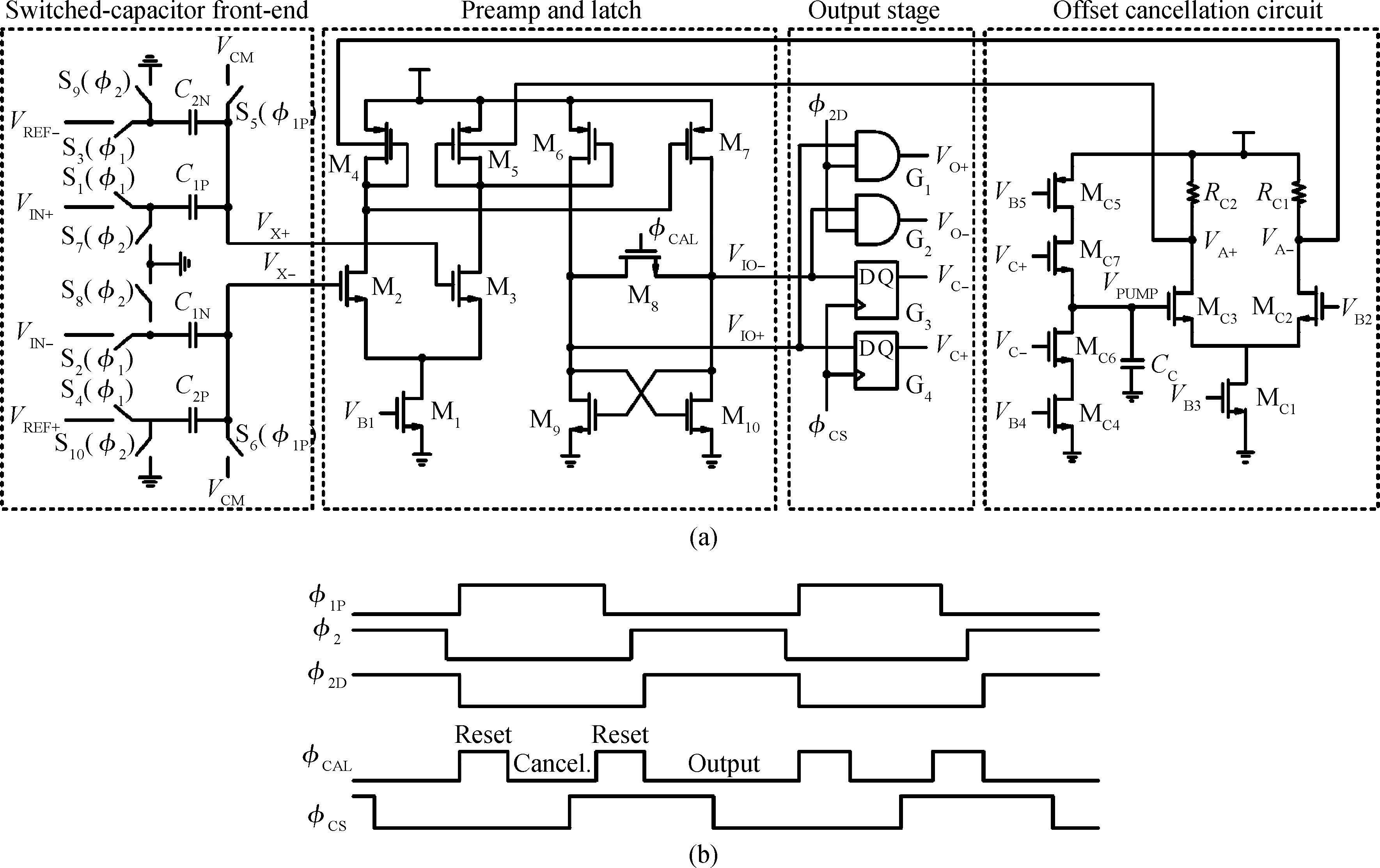
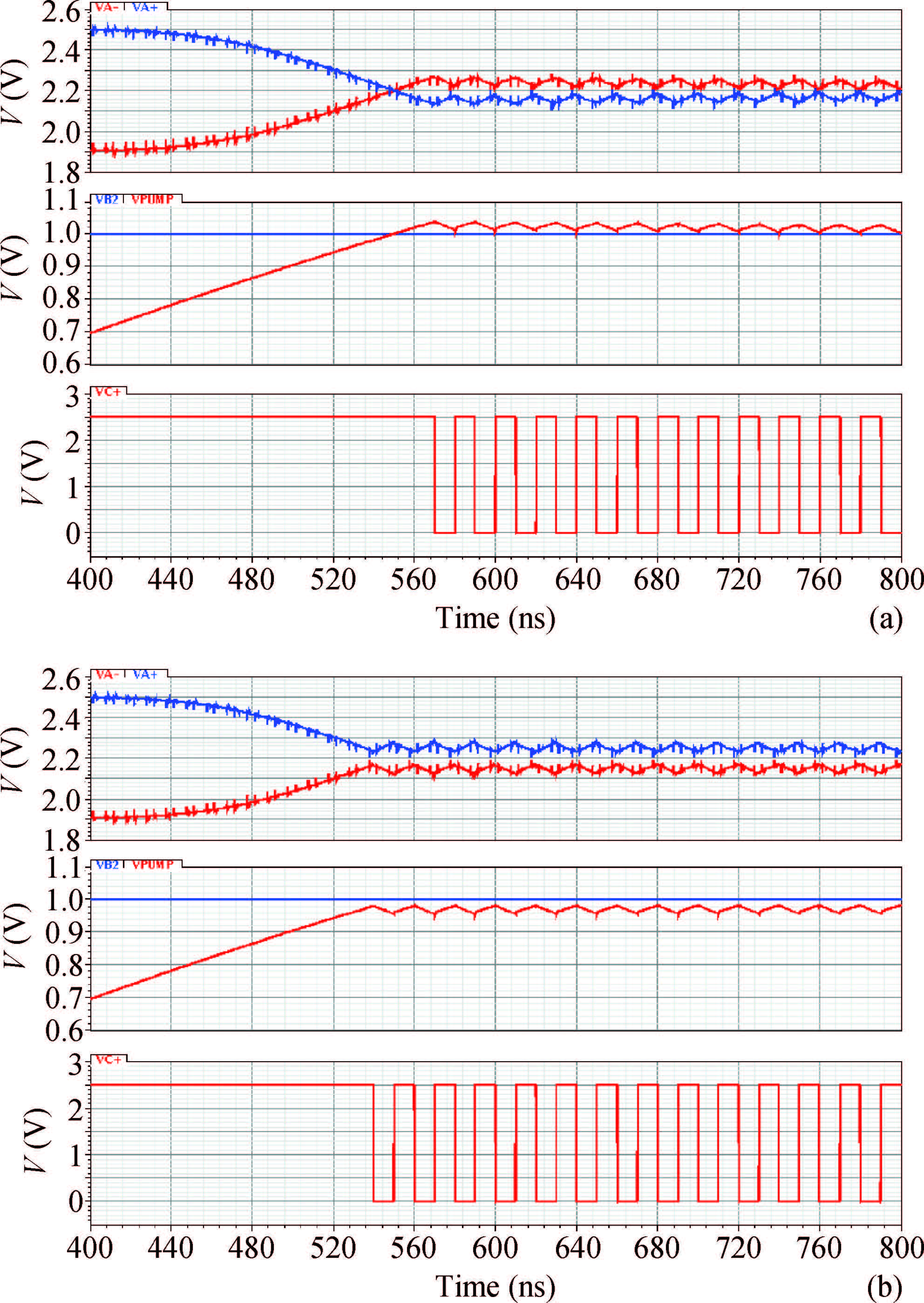
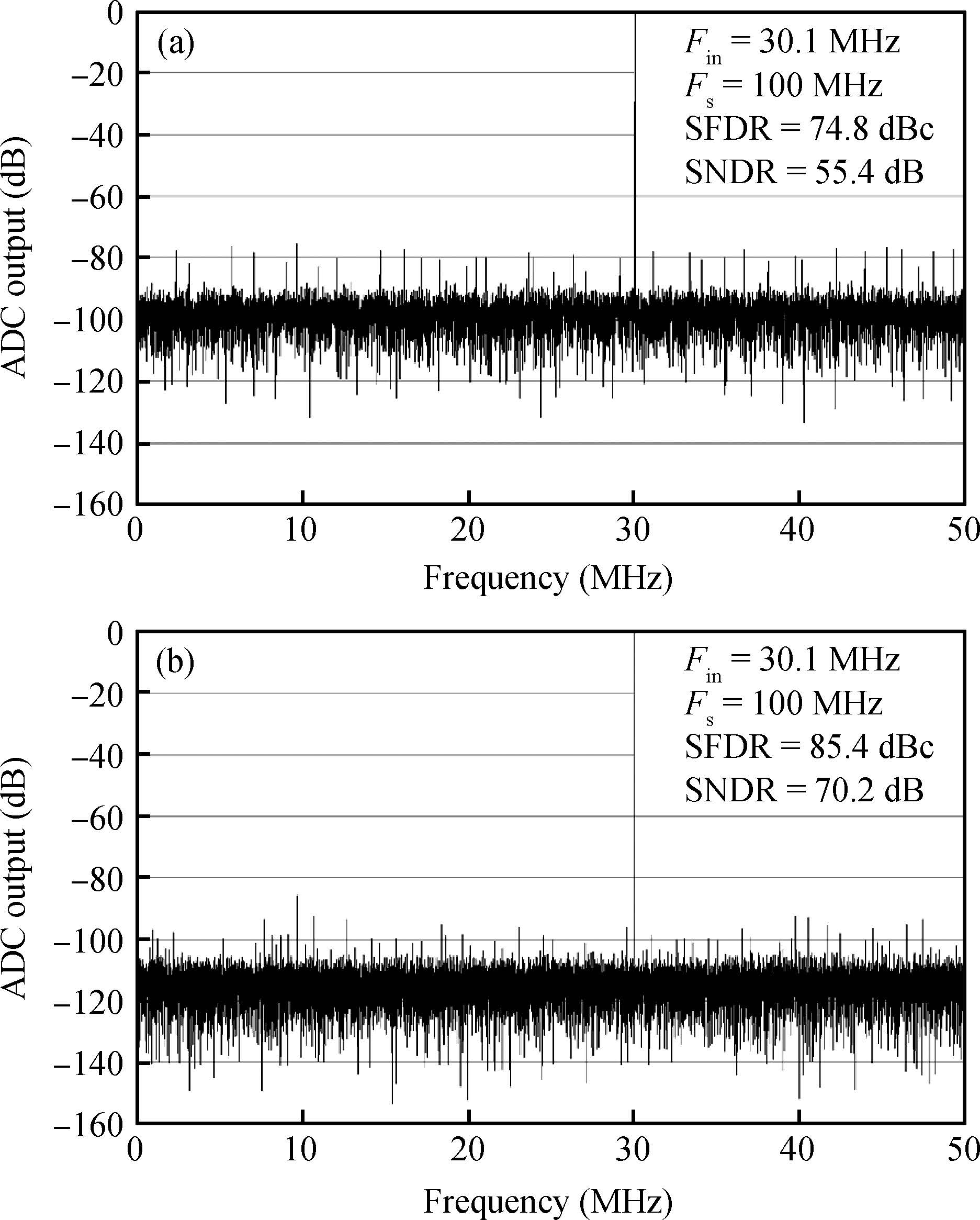
Abstract: A 14-bit 100-MS/s pipelined analog-to-digital converter(ADC) without dedicated front-end sample-and-hold amplifier(SHA) is presented. In addition to elaborate matching of the sampling network in the first stage, a background offset cancellation circuit is proposed in this paper to suppress the offset of the comparators in the first-stage sub-ADC, which ensures the overall offset does not exceed the correction range of the built-in redundant structure. Fabricated in a 0.18-μm CMOS technology, the presented ADC occupies a chip area of 12 mm2, and consumes 237 mW from a 1.8-V power supply. Measurement results with a 30.1-MHz input sine wave under a sampling rate of 100 MS/s show that the ADC achieves a 71-dB signal-to-noise and distortion ratio(SNDR), an 85.4-dB spurious-free dynamic range(SFDR), a maximum differential nonlinearity(DNL) of 0.22 LSB and a maximum integral nonlinearity(INL) of 1.4 LSB.
Keywords: SHA-less, pipelined ADC, clock skew, comparator offset, background
| [1] | |
| [2] | |
| [3] | |
| [4] | |
| [5] | |
| [6] | |
| [7] | |
| [8] | |
| [9] | |
| [10] |
| [1] | |
| [2] | |
| [3] | |
| [4] | |
| [5] | |
| [6] | |
| [7] | |
| [8] | |
| [9] | |
| [10] |


Article views: 5031 Times PDF downloads: 82 Times Cited by: 0 Times
Received: 25 July 2015 Revised: Online: Published: 01 March 2016
| Citation: |
Xiaofei Wang, Hong Zhang, Jie Zhang, Xin Du, Yue Hao. A SHA-less 14-bit, 100-MS/s pipelined ADC with comparator offset cancellation in background[J]. Journal of Semiconductors, 2016, 37(3): 035002. doi: 10.1088/1674-4926/37/3/035002
****
X F Wang, H Zhang, J Zhang, X Du, Y Hao. A SHA-less 14-bit, 100-MS/s pipelined ADC with comparator offset cancellation in background[J]. J. Semicond., 2016, 37(3): 035002. doi: 10.1088/1674-4926/37/3/035002.

|
| [1] | |
| [2] | |
| [3] | |
| [4] | |
| [5] | |
| [6] | |
| [7] | |
| [8] | |
| [9] | |
| [10] |

 WeChat ID
Journal of Semiconductors © 2017 All Rights Reserved 京ICP备05085259号-2

 DownLoad: