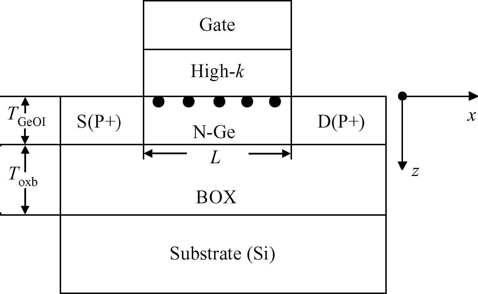
Loading [MathJax]/jax/output/HTML-CSS/jax.js
J. Semicond. > 2016, Volume 37 > Issue 4 > 044004

SEMICONDUCTOR DEVICES

A physical model of hole mobility for germanium-on-insulator pMOSFETs

Wenyu Yuan, Jingping Xu, Lu Liu, Yong Huang and Zhixiang Cheng

+ Author Affiliations

 Corresponding author: Jingping Xu, Email:jpxu@hust.edu.cn

DOI: 10.1088/1674-4926/37/4/044004

PDF

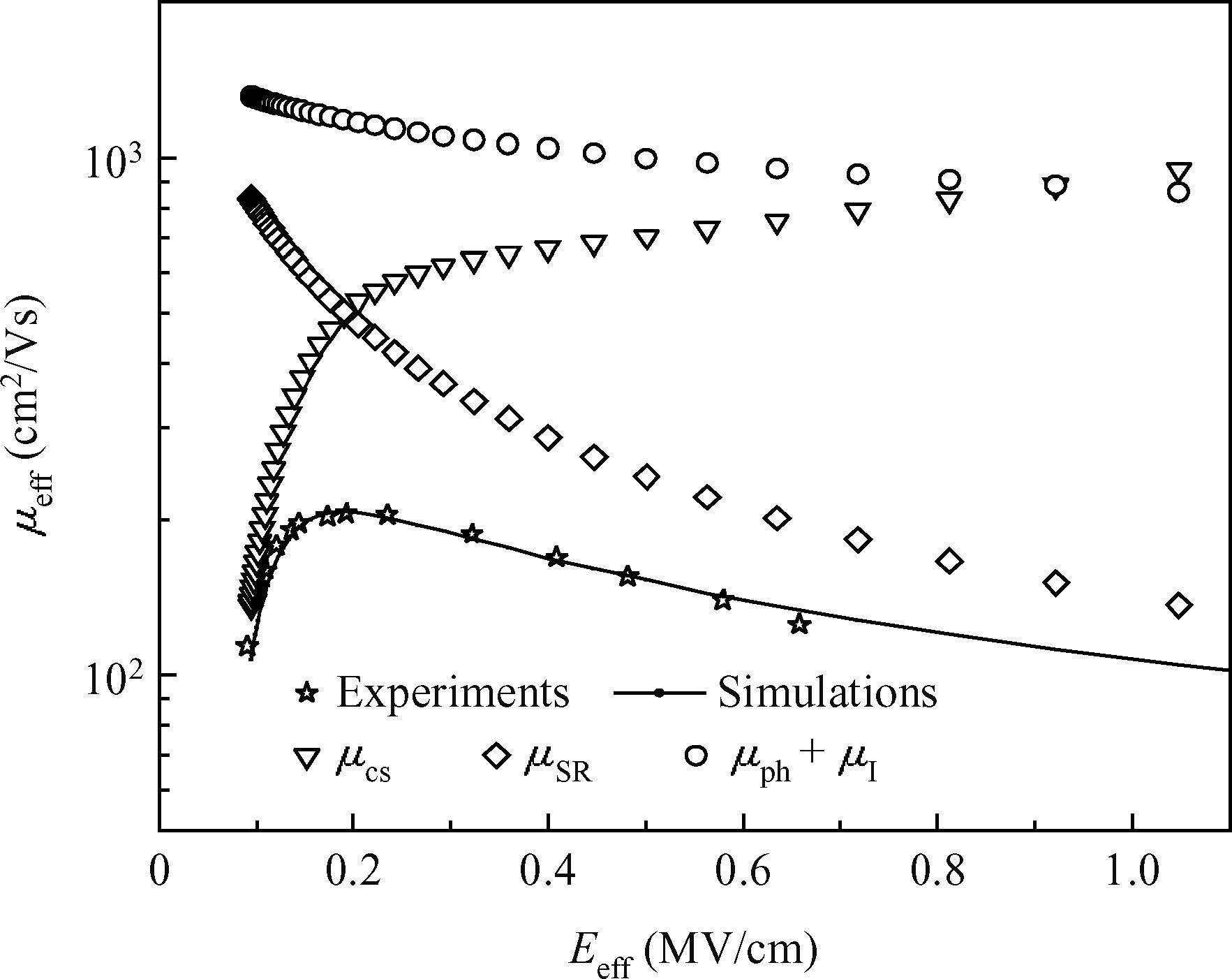
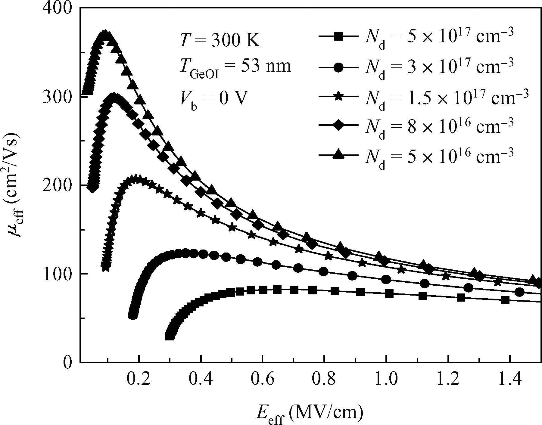
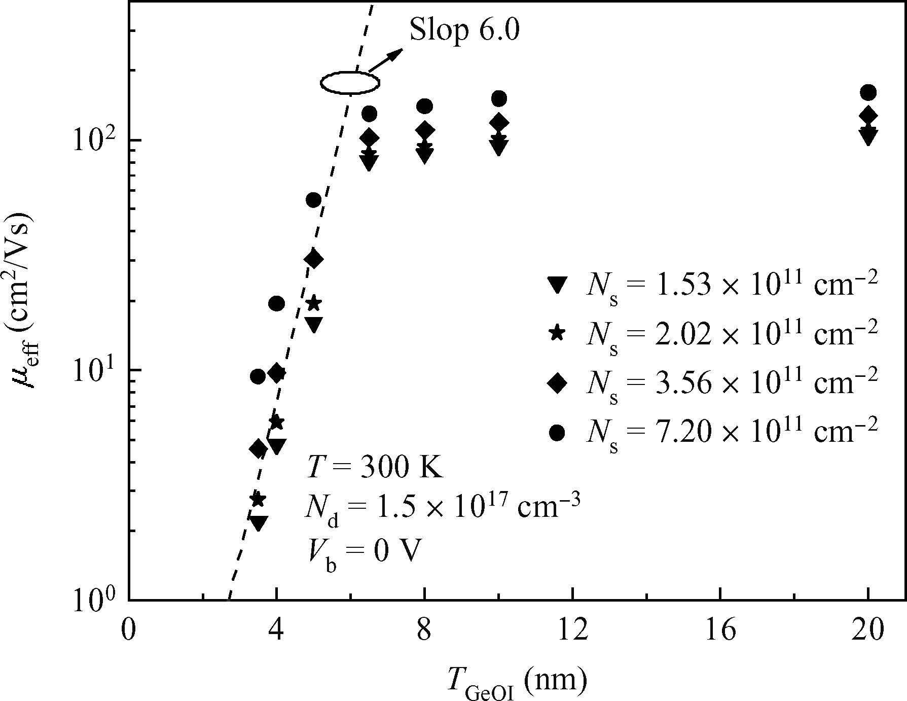
Abstract: A physical model of hole mobility for germanium-on-insulator pMOSFETs is built by analyzing all kinds of scattering mechanisms, and a good agreement of the simulated results with the experimental data is achieved, confirming the validity of this model. The scattering mechanisms involved in this model include acoustic phonon scattering, ionized impurity scattering, surface roughness scattering, coulomb scattering and the scattering caused by Ge film thickness fluctuation. The simulated results show that the coulomb scattering from the interface charges is responsible for the hole mobility degradation in the low-field regime and the surface roughness scattering limits the hole mobility in the high-field regime. In addition, the effects of some factors, e.g. temperature, doping concentration of the channel and the thickness of Ge film, on degradation of the mobility are also discussed using the model, thus obtaining a reasonable range of the relevant parameters.

Key words: GeOIpMOSFETshole mobilityscattering mechanisms

With silicon CMOS devices scaled into the deep submicrometer regime,using Ge as the channel material to fabricate germanium-on-insulator (GeOI) MOSFETs has become a hot research topic,due to its high mobility and performances[1, 2, 3, 4, 5, 6],in which the carrier mobility in the channel is one of the most concerned topics. In 2008,Bedell et al. demonstrated that high hole mobility can be maintained with the gate lengths down to 65 nm in partially strained (0.5%) Ge p-channel MOSFETs fabricated on silicon-germanium-on-insulator (SGOI) substrates[7]. In 2010,Gu et al. used ultra-thin thermal GeO2 as the passivation layer to prepare GeOI pMOSFETs with a high quality interface and obtained a peak hole mobility of 260 cm2/(Vs) at room temperature[8]. In 2013,Lee et al. investigated the depth profiling of GeOI crystallinity by using Raman spectroscopy and confirmed that the difference of Ge crystallinity in the front channel from that in the back one was an important mechanism of mobility degradation in ultra-thin body GeOI nMOSFETs[9]. In 2014,Hosoi et al. reported a very high peak hole mobility of 511 cm2/(Vs) in pseudo-GeOI pMOSFETs with back-gate controlled striped Ge channels fabricated by lateral liquid-phase epitaxy (LLPE),showing that LLPE is a promising technique to prepare next-generation GeOI MOS devices with high mobility[10].

Although many fruitful results have been achieved in the experimental investigation on carrier mobility of GeOI MOSFETs,the theoretical model on the mobility was less involved. In 2011,Daele[11] presented a simple empirical model on the hole mobility,but the micro-physical mechanisms could not be clearly revealed by his model. So,the aim of this work is to establish a physically based hole mobility model of GeOI pMOSFETs by comprehensively analyzing the scattering mechanisms,e.g. acoustic phonon scattering,ionized impurity scattering,surface roughness scattering,coulomb scattering,and so on. The correctness and validity of the model are confirmed by comparing with experimental data. Moreover,some useful results are obtained by using this model to discuss the effects of temperature,surface roughness,the interface charges,channel doping concentration and the thickness of Ge film on inversion channel mobility of GeOI pMOSFETs in detail.

The structure of GeOI pMOSFETs is shown in Figure1,where TGeOI and Toxb are the thicknesses of the n-type Ge film and buried oxide layer,respectively,L is the channel length,and a high-k material is used as the gate dielectric. Based on Fermi's Golden Rule[12],the scattering probability of carriers in semiconductors can be expressed as:

Pkk=1τkk=2π|Mkk|2δ(EkEk±w),

where Pkk is the scattering probability of carriers from the k state to the k state,τkk is the relaxation time,Mkk is the scattering matrix element,the δ function is the condition for energy conservation,while and ω are the Planck constant and the phonon frequency (ω is phonon energy),respectively. When the elastic scattering happens on the carriers,ω equals to zero. Fortunately,the ionized impurity scattering is elastic scattering and acoustic phonons scattering can be approximately treated as elastic scattering because the energy of electrons or holes is higher than that of the phonons so that when electrons or holes are scattered by phonons,their energy change can be ignored as compared with their average energy.

Figure  1.  The schematic diagram of a GeOI pMOSFET structure.

In the following paragraphs,the effects of different scattering mechanisms on the hole mobility in the inversion channel will be investigated in detail.

Assuming that hole carriers in the inversion layer are two-dimensional hole gas and occupy only the lowest subband,the mobility determined by acoustic phonon scattering can be described as follows[13, 14]:

Pac=1τac=mdD2ackbT3ρv2s|ζm(z)|2|ζn(z)|2dz,

and the corresponding hole mobility can be calculated as:

μac=eτacm,

where τac is the relaxation time of acoustic phonon scattering,md and m are the density-of-state mass and conductivity mass,respectively; e is the elemental charge,Dac is the deformation potential for the acoustic phonon scattering,ρ is the density of Germanium,vs is the velocity of phonons in Ge with v2s=v2l+v2t[15] (vl and vt are the longitudinal and transverse velocity of phonons,respectively),ζm(z) and ζn(z) are the envelope function of two dimensional carriers in m-th and n-th subband. According to the results given by Stern and Howard[16],the integral in Equation (2) can be rewritten as:

(|ζm(z)|2|ζn(z)|2dz)1=163(ε0εs212me2)1/3×(Ndepl+1132Ns)1/3,

where Ns and Ndepl are the inversion-charge areal density and effective depletion-charge areal density,respectively,while ε0 and εs are the vacuum permittivity and the relative permittivity of Ge,respectively. In fact,the hole mobility described by Equation (2) is related to the effective electric field (Eeff) at the high-k/Ge interface[17]:

Eeff=eε0εs(Ndepl+ηNs)+εoxbεsVbToxb,

where εoxb is the relative permittivity of the buried oxide layer,Vb is the substrate bias and the η factor is 1/3 for holes in bulk Si and Ge[18],however,it changes slightly with the inversion-charge areal density in GeOI MOSFETs,implying that the η factor depends on device architecture,and its average value for GeOI MOSFETs is found to be around 0.40[11]. Besides,as can be seen from Eq. (5),Eeff is also a function of Ns.

Brooks-Herring approximation can be used to describe the ionized impurity scattering when the doping concentration of the channel is below 1018 cm3. The screening coulomb potential in a nondegenerate case can be expressed as:

V(r)=e4πε0εsrexp(βsr), β2s=ne2ε0εskbT,

where βs is the inverse screening length and n is the concentration of ionized impurity.

According to Reference [19],the Brooks-Herring formula can be written as:

PI=1τI=V4π2k11(1ξ)Pi(k,k)k2dkdξ, Pi(k,k)=2πNe2V|V(q1)|2δ(EkEk), V(q1)=V(r)exp(iq1r)dr,

in which V(q1) is the Fourier coefficient of V(r),Pi(k,k) is the scattering probability of the holes per unit volume by the ionized impurity scattering center and τI is the relevant scattering relaxation time. Substituting Equations (6),(7),(9) and (10) into Equation (8) and using the formula of μI=eτIm,the mobility limited by ionized impurity scattering can be worked out:

μI=162π(ε0εs)2E3/20Nde3m1/2[ln(1+a)a1+a]1,

where a=8mE02β2s,Nd is the doping concentration in the channel (assuming that all the impurities are ionized at room temperature,then n=Nd),and E0 is the thermal energy (E0 = 3/2kbT[15]). The Born approximation presupposes that a 1,so that the quantity within the bracket in Equation (11) may be replaced by lna[19]. Thus,Equation (11) can be rewritten as:

μI=162π(ε0εs)2E3/20Nde3m1/2lna.

Assuming that Δ(r) is a thickness deviated from its average position,as shown in Figure2,the perturbation Hamiltonian can be calculated by[20]:

HSR=eV(z)eV[z+Δ(r)]=eΔ(r)tialV(z)tialz=eΔ(r)Eeff.

Figure  2.  Schematic model for the roughness of the high-k dielectric/Ge interface,in which the dashed line represents the average position of the interface.

Assuming that the correlation function C(r)=Δ(r),Δ(r+r) described the roughness obeys the exponential distribution,the power spectral density can be found by Fourier transform of C(r)[21]:

S(q2)=πΔ2l2(1+q22l22)3/2,

where q2 = 2kFsinθ/2,kF is the Fermi wavenumber,while and l are the average deviation and the correlation length of the high-k dielectric/Ge interface,respectively. Thus,the scattering probability and relaxation time of the surface roughness scattering can be obtained through finding the scattering matrix element by substituting the Fourier transform of HSR and Equation (14) into Equation (1). Further,according to the formula of μsr=eτsrm,the mobility limited by surface roughness scattering can be described as:

1μsr=emdmE2effπ32π0(1cosθ)S(q2)dθ.

Assuming that an interface charge is located at z=z0 along the high-k/Ge interface,the perturbation electrostatic potential caused by this charge can be obtained by solving Poisson' equation:

[ε(z)(r,z)]=(ρ0+ρind),

where ρ0 and ρind are the interface charges density and induced screening-charge density[20],respectively,and ε(z) is the position-dependent permittivity overall. According to the results of Ando[20],the coulomb scattering matrix element can be expressed as:

Mcs(q3)=Niteε012(εox+εs)P0eq3z0q3+qs(Pav+δsP20),

δs=εsεoxεs+εox,

qs(q3)=e2md4πε0εs210f(b1xEf/kBT)1xdx,

P0=b3(b+q3)3,Pav=8b3+9b2q3+3bq238(b+q3)3,

b=[12e2md(Ndepl+1132Ns)/(ε0εs2)]1/3,

where f is the Fermi Dirac distribution,Ef is the Fermi level,b1=q28mdkbT,qs is the wave-vector-dependent screening parameter,b is a variational parameter,Nit is the areal density of the interface charges and q3 $=k’- k is the change of wavenumber before and after scattering. Then,the scattering probability of the coulomb scattering can be written as:

Pcs(E)=1τ(E)=mdπ3π0|Mcs(q3)|2(1cosϕ)dϕ.

Thus,the averaged relaxation time over kinetic energy E can be described as:

1τcs=E1Eτ(E)tialftialEdEE1f(E)dE,

where E1 denotes the ground level of the first subband. Hence,the mobility limited by coulomb scattering can be calculated by μcs=eτcsm.

Aside from the mechanisms mentioned above,the thickness of Ge film and the interface quality between the Ge film and the buried oxide layer in GeOI MOSFETs also have effects on the carrier mobility in the inversion channel. The smaller the thickness of Ge film (TGeOI) is,the more degraded the mobility is,due to the dominated scattering from the fixed charge at the Ge/buried oxide layer interface[17, 22] and from the quantum well produced by ultra-thin Ge film[23, 24]. Besides,the scattering potential for a hole in the i-th subband (i = 1,2,3,) produced by a variation of TGeOI can be expressed as[25]:

VFLi(r)(dEidTGeOI)ΔFL(r),

where Ei is the eigenvalue of the subband and ΔFL(r) is the TGeOI variation in the transport plane. Further,the scattering probability (reciprocal relaxation time) induced by the additional potential can be derived as:

PGeOI=1τGeOI=mdπ3(dEidTGeOI)2π0SFL(q4)ε2(q4)(1cosϕ)dϕ,

where dEidTGeOI=π22i2mT3GeOI,SFL(q4) is the power spectrum density of the TGeOI fluctuations[25],and ε(q4) is the two-dimensional static dielectric function[26]. So,the mobility limited by the TGeOI variation can be obtained by μtGeOI=eτGeOIm.

Obviously,the mobility is roughly proportional to T6GeOI.

Based on Matthiessen's rule,the total effective mobility μeff of holes in the inversion channel limited by all the above mechanisms can be calculated as: 1μeff=1μph+1μI+1μsr+1μcs+1μtGeOI.

In simulation,a part of the physical parameters of GeOI pMOSFETs,e.g. TGeOI = 53 nm,Toxb = 147 nm,CET = 2.1 nm (capacitance equivalent thickness),εox = 10.2,εoxb = 3.9,etc.,are the same as those in Reference [27],and the other parameters,e.g. η,Dac,ρ,εs,etc.,are from References [11, 15, 28],or are determined by fitting with experimental results,e.g. Δ,l,Nit ,etc.,as listed in Table1.

Table  1.  A part of the physical parameters used in simulation.
DownLoad: CSV  | Show Table

Figure3 shows a comparison between the simulated hole mobility and experimental data. For clearly analyzing the effects of the scattering mechanisms on hole mobility,the mobilities limited by different mechanisms are respectively plotted in Figure3,in which the hollow circles represent the mobility determined by the phonon and ionized impurity scattering,i.e.,bulk-lattice scattering mobility; the triangle symbol is the mobility limited by the coulomb scattering; the diamond symbol describes the mobility affected by the surface roughness scattering and the black solid line stands for the effective mobility calculated by Equation (26). As shown in Figure3,a good agreement of the simulated results with experimental data[27] is achieved. The slightly larger values than the experiment data under high fields originated from the fact that only a first-order approximation of the Taylor formula was employed when calculating the perturbation Hamiltonian in Equation (13). It can be observed from Figure3 that in the low-field regime,the coulomb scattering is the main limiting mechanism because as the electrical field increases in the low-field regime,the carrier density in the inversion channel is increased,which makes the coulomb screening parameter qs [Equation (19)] and the variational parameter b [Equation (21)] enhanced,increasing the carrier mobility; in the high-field regime,the surface roughness scattering becomes the dominant mechanism because a highly effective electric field would induce a large perturbation potential at the roughness surface,which produces a strong scattering on the transportation of holes in the inversion layer,thus leading to a reduction of the hole mobility. While the acoustic phonon scattering is dependent on temperature,the ionized impurity scattering is related to temperature and the doping concentration of the channel would mainly affect the peak value of the hole mobility,they are less sensitive to the effective electric field.

Figure  3.  Comparison between the simulated hole mobilities and the experimental data for GeOI pMOSFETs.

Normally,it is believed that the impurities in Ge are fully ionized at room temperature. So,the perturbation potential is increased as the doping concentration increases,which makes the ionized impurity scattering on carriers enhanced,thus degrading the mobility,as shown in Figure4. The hole mobility in the high-field regime tends to be consistent because the surface roughness is assumed to be the same,which is similar to that in Reference [29] (for Ge film thickness of 20-60 nm). However,the doping concentration of the channel should not be too low for suppressing the short channel effect[30]. In addition,it can be seen from Figure4 that the curves of mobility versus Eeff right shift as Nd increases,because a higher electric field is needed to realize the inversion of the channel as doping concentration increases.

Figure  4.  Hole mobility versus the effective electric field under different doping concentrations of the channel.

Figure5 depicts the change of the hole mobility with effective electric field for different Δ parameters. In the low-field regime,the change trend of hole mobility for different Δ parameters tends to be consistent since the coulomb scattering is the dominant mechanism,and nevertheless,the hole mobility is greatly degraded in the high-field regime as Δ increases since the surface roughness scattering plays a main role in this case,as mentioned above.

Figure  5.  Hole mobility versus the effective electric field for various surface roughness.

As compared with the Δ parameter,the correlation length (l) has a smaller effect on the channel-hole mobility. However,for a given Eeff or Ns,the power spectral density in Equation (13) is maximum when l=12kFsinθ2,and hence the surface roughness scattering is strongest. The above condition implies that when Ns = 8 × 1012 cm2,l is 2 nm,comparable to the thermal DE Broglie wavelength (k1th 2 nm)[31]. So,a smooth surface is very necessary to obtain a high mobility.

Figure6 is the hole mobility as a function of Eeff under different temperatures. Obviously,the hole mobility is decreased with the elevating temperature. This is because the lattice vibration is enhanced as temperature increases,which makes the phonon scattering increased. Under low temperatures (< 300 K),the ionized impurity concentration is increased with elevated temperature and accordingly,the ionized impurity scattering on channel carriers is gradually enhanced. Therefore,both the acoustic phonon scattering and the ionized impurity scattering become the dominant mechanisms at low temperatures. While temperature is above room temperature,all the impurities are fully ionized so that only acoustic phonon scattering is the main mechanism to limit the mobility,resulting in a weakened temperature dependence of the hole mobility,as shown in Figure6.

Figure  6.  Hole mobility versus the effective electric field under different temperatures.

The interface charges generate coulomb potential and hence give rise to coulomb scattering on hole carriers,leading to a lower mobility. As can be seen from Figure7,the higher the interface-charge areal density is,the lower the low-field hole mobility is,while the degradation of the high-field hole mobility gradually tends to be consistent because it is mainly determined by the surface roughness scattering,as mentioned above. In addition,the right shift of the mobility versus Eeff curves with the increase of the interface charges areal density is attributed to the increased threshold voltage of the device,which is obviously not beneficial to a reduction of power consumption. Therefore,a high quality high-k/Ge interface is highly desired to improve the carrier mobility in the inversion channel.

Figure  7.  Hole mobility versus the effective electric field under different interface charge areal densities.

Figure8 shows the TGeOI dependence of the hole mobility in the inversion channel. When TGeOI > 10 nm,the mobility hardly changes with the thickness of the Ge film,and when TGeOI < 10 nm,the mobility is obviously decreased as TGeOI decreases and especially when TGeOI < 5 nm,a serious degradation of the mobility is observed. This is because a very strong quantum well effect will appear in the case of TGeOI < 10 nm especially TGeOI < 5 nm,which will create a large additional potential[32] and a strong scattering on the channel carriers,resulting in an obvious reduction of the mobility in the low-field regime. In addition,this kind of scattering is inherently related to the size-induced quantization in the Ge film[25],which is different from the mechanism of the surface roughness scattering described in Section 2.3. Further,Figure9 illustrates a strong dependence between the mobility and TGeOI under the weak fields or low inversion-charge densities. As can be seen,for TGeOI < 5 nm,the hole mobility decreases with T6GeOI,which is also explained in Reference [25]. On the contrary,a gradually weakened thickness dependence of the hole mobility can be found for TGeOI > 5 nm,e.g. TGeOI = 6.5,8,10 nm,etc. So,the thickness of Ge film is an important parameter in GeOI pMOSFETs.

Figure  8.  Hole mobility versus the effective electric field for different thicknesses of Ge film.
Figure  9.  Hole mobility versus thickness of Ge film for different inversion charge densities under the weak fields.

On the other hand,too thin Ge film would make the inversion channel closer to the buried oxide interface,which makes the channel carriers easily suffer from scattering of the fixed charge of the buried oxide layer,leading to a further reduction of the hole mobility,as calculated in Reference [22]. Therefore,in order to prevent the serious degradation of the hole mobility in the inversion layer,the thickness of the Ge film should not be too thin,for example,TGeOI = 10 nm.

Based on Fermi's Golden Rule,a physical model of the hole mobility for GeOI pMOSFETs has been established by comprehensively considering various kinds of scattering mechanisms. The validity of the model is confirmed by the relevant experimental data. Using the model,the physical mechanisms on the degradation of the mobility under different conditions are analyzed,and the simulation results show that (i) in the low-field regime,the hole mobility is determined by the coulomb scattering and the larger the interface-charge areal density is,the more serious the mobility degradation is; (ii) in the high-field regime,surface roughness scattering is the dominant mechanism on the degradation of the mobility and the smoother the surface is,the higher the mobility is; (iii) the acoustic phonon scattering becomes strong with elevated temperature,and at low temperatures,the ionized impurity scattering is also an important scattering mechanism besides the acoustic phonon scattering; (iv) a higher doping concentration of the channel could generate a more serious ionized impurity scattering,resulting in a lower hole mobility,however,to suppress the short channel effect,the doping concentration should not be too low; (v) in the case of TGeOI < 10 nm,the scattering potential from the quantum well could induce a severe degradation of the hole mobility,and to maintain a high mobility,a TGeOI of 10 nm is reasonable. In summary,a smooth surface,high quality high-k/Ge interface,reasonable doping concentration of the channel and thickness of Ge film are highly desired for enhancing the hole mobility of GeOI pMOSFETs.


[1]
[2]
[3]
[4]
[5]
[6]
[7]
[8]
[9]
[10]
[11]
[12]
[13]
[14]
[15]
[16]
[17]
[18]
[19]
[20]
[21]
[22]
[23]
[24]
[25]
[26]
[27]
[28]
[29]
[30]
[31]
[32]
Fig. 1.  The schematic diagram of a GeOI pMOSFET structure.

Fig. 2.  Schematic model for the roughness of the high-k dielectric/Ge interface,in which the dashed line represents the average position of the interface.

Fig. 3.  Comparison between the simulated hole mobilities and the experimental data for GeOI pMOSFETs.

Fig. 4.  Hole mobility versus the effective electric field under different doping concentrations of the channel.

Fig. 5.  Hole mobility versus the effective electric field for various surface roughness.

Fig. 6.  Hole mobility versus the effective electric field under different temperatures.

Fig. 7.  Hole mobility versus the effective electric field under different interface charge areal densities.

Fig. 8.  Hole mobility versus the effective electric field for different thicknesses of Ge film.

Fig. 9.  Hole mobility versus thickness of Ge film for different inversion charge densities under the weak fields.

Table 1.   A part of the physical parameters used in simulation.

DownLoad: CSV
[1]
[2]
[3]
[4]
[5]
[6]
[7]
[8]
[9]
[10]
[11]
[12]
[13]
[14]
[15]
[16]
[17]
[18]
[19]
[20]
[21]
[22]
[23]
[24]
[25]
[26]
[27]
[28]
[29]
[30]
[31]
[32]
  • Search

    Advanced Search >>

    GET CITATION

    shu

    Export: BibTex EndNote

    Article Metrics

    Article views: 3112 Times PDF downloads: 38 Times Cited by: 0 Times

    History

    Received: 30 July 2015 Revised: Online: Published: 01 April 2016

    Catalog

      Email This Article

      User name:
      Email:*请输入正确邮箱
      Code:*验证码错误
      Wenyu Yuan, Jingping Xu, Lu Liu, Yong Huang, Zhixiang Cheng. A physical model of hole mobility for germanium-on-insulator pMOSFETs[J]. Journal of Semiconductors, 2016, 37(4): 044004. doi: 10.1088/1674-4926/37/4/044004 ****W Y Yuan, J P Xu, L Liu, Y Huang, Z X Cheng. A physical model of hole mobility for germanium-on-insulator pMOSFETs[J]. J. Semicond., 2016, 37(4): 044004. doi: 10.1088/1674-4926/37/4/044004.
      Citation:
      Wenyu Yuan, Jingping Xu, Lu Liu, Yong Huang, Zhixiang Cheng. A physical model of hole mobility for germanium-on-insulator pMOSFETs[J]. Journal of Semiconductors, 2016, 37(4): 044004. doi: 10.1088/1674-4926/37/4/044004 ****
      W Y Yuan, J P Xu, L Liu, Y Huang, Z X Cheng. A physical model of hole mobility for germanium-on-insulator pMOSFETs[J]. J. Semicond., 2016, 37(4): 044004. doi: 10.1088/1674-4926/37/4/044004.

      A physical model of hole mobility for germanium-on-insulator pMOSFETs

      DOI: 10.1088/1674-4926/37/4/044004
      Funds:

      Project supported by the National Natural Science Foundation of China (Nos. 61274112, 61176100, 61404055).

      More Information
      • Corresponding author: Email:jpxu@hust.edu.cn
      • Received Date: 2015-07-30
      • Accepted Date: 2015-10-14
      • Published Date: 2016-01-25

      Catalog

        /

        DownLoad:  Full-Size Img  PowerPoint
        Return
        Return