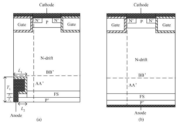
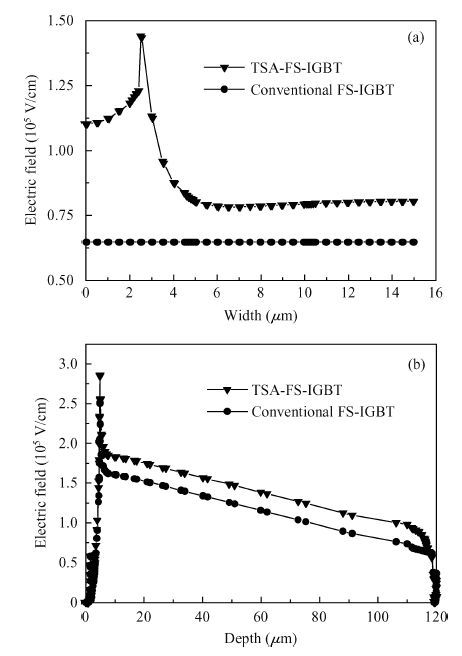
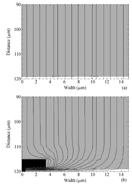
Processing math: 100%
J. Semicond. > 2016, Volume 37 > Issue 5 > 054008

SEMICONDUCTOR DEVICES

Novel trench gate field stop IGBT with trench shorted anode

Xudong Chen1, , Jianbing Cheng1, 2, Guobing Teng1 and Houdong Guo1

+ Author Affiliations

 Corresponding author: Corresponding author. Email: xdcnjupt@163.com

DOI: 10.1088/1674-4926/37/5/054008

PDF

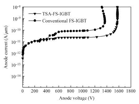
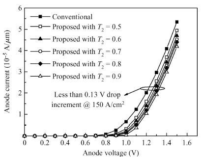
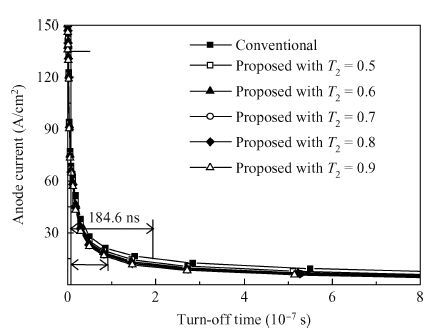
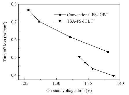
Abstract: A novel trench field stop (FS) insulated gate bipolar transistor (IGBT) with a trench shorted anode (TSA) is proposed. By introducing a trench shorted anode, the TSA-FS-IGBT can obviously improve the breakdown voltage. As the simulation results show, the breakdown voltage is improved by a factor of 19.5% with a lower leakage current compared with the conventional FS-IGBT. The turn off time of the proposed structure is 50% lower than the conventional one with less than 9% voltage drop increased at a current density of 150 A/cm2. Additionally, there is no snapback observed. As a result, the TSA-FS-IGBT has a better trade-off relationship between the turn off loss and forward drop.

Key words: FS-IGBTtrench shorted anodebreakdown voltageturn off losstradeoff

Insulated gate bipolar transistors (IGBTs) have been widely used to power electronic applications such as motor control and electrical drive circuits[1, 2]. The major target of IGBT design is to improve the breakdown voltage and realize a better trade-off between forward drop and turn off loss. Great efforts have been made to optimize these performances of IGBTs. Field stop (FS) and trench gate structure have been used to significantly improve performances of IGBT[3, 4]. To further lower the switching speed, various concepts including shorted anode[5, 6], striped anode[7], segmented anode[8], injection efficiency controlled IGBT[2, 9], dual-gates structure[10, 11, 12], n-region controlled[13] and super junction IGBT[14, 15] have also been introduced.

This paper proposes a novel trench shorted anode FS IGBT (TSA-FS-IGBT) structure. Extensive numerical simulations are carried out to analyze performances of the new structure. Comparison results between the TSA-FS-IGBT and conventional FS-IGBT are also discussed.

A schematic cross section of the proposed TSA-FS-IGBT and a conventional FS-IGBT is shown in Figure 1. The major difference between the two devices is that the TSA-FS-IGBT has a trench shorted anode. The new anode design modulates the electric field in the drift region. Consequently, the breakdown voltage is improved compared with the conventional device.

Figure  1.  Schematic cross-section of (a) the proposed TSA-FS-IGBT and (b) conventional FS-IGBT.

When the gate applied voltage is higher than the threshold voltage, the TSA-FS-IGBT turns on. If the anode bias voltage is small, it operates in unipolar mode because the n-drift is shorted to the anode. When the channel current is large enough, the PN junction (P+ anode/shorted N-drift) is forward biased, holes start to inject into the drift region. Then the TSA-FS-IGBT operates into bipolar mode. During turn off, electrons are extracted faster than the conventional FS-IGBT due to the shorted electron extraction path.

The device parameters used in the simulation are listed in Table1. Physical models used include the concentration dependent model, the perpendicular electric field model, the band gap narrowing model, the auger combination model, the Shockley-Read-Hall recombination model and the impact ionization model. The excess carrier lifetime is set to 1.2 μs (τn = 2τp) for both structures.

Table  1.  Device specification.
DownLoad: CSV  | Show Table

Figure 2 shows the forward blocking characteristic of the TSA-FS-IGBT and conventional FS-IGBT. The two devices are designed to realize the blocking class of 1.2 kV. Figure 2 shows the breakdown voltage for the conventional FS-IGBT is 1316 V while the TSA-FS-IGBT is 1573 V, which is 257 V higher. In addition, the TSA-FS-IGBT has a lower leakage current because the introduction of the trench anode reduces the anode injection efficiency and the transport factor of the PNP transistor.

Figure  2.  Blocking characteristics of different structures. T2 = 0.7 μm, L2 = 2 μm and T1 = 5 μm for the TSA-FS-IGBT.

Figure 3 shows the lateral electric field and the vertical electric field distribution at cut line BB' and AA'. The lateral electric field of the TSA-FS-IGBT is obviously higher than the conventional one from Figure 3(a). An electric field peak appears at 2.5 μm, because the electric field is concentrated at the trench oxide corner. Figure 3(b) shows the vertical electric field of the proposed structure is a little higher than that of the conventional FS-IGBT. An enhanced electron accumulation layer is formed around the anode trench oxide when the forward blocking voltage is biased at the shorted anode. Firstly, the electron accumulation layer stops the electric field just like the FS layer. Secondly, the electron accumulation layer around the trench oxide helps to compensate partial positive charges in the fully depleted FS layer[16]. Thus, the electric field can be modulated to a higher level as seen from Figure 3. Therefore, the TSA-FS-IGBT can sustain a higher blocking voltage.

Figure  3.  (a) Lateral electric field along BB' and (b) vertical electric field along AA' of TSA-FS-IGBT (T1 = 0.7 μm, L2 = 2 μm and T1 = 5 μm) and conventional FS-IGBT.

The I-V characteristic of the TSA-FS-IGBT is strongly dependent on the parameter L2 and T2. The minimum voltage for generating the hole injection across the shorted drift region Vsd is expressed as:

Vsd = IchL2qNdμnT2w,
(1)
where Ich is the channel current, q is the electron charge, Nd is the drift region doping concentration, and μn is the electron mobility. And w equals to 1 μm, which is the device width in the third dimension. As for the TSA-FS-IGBT, because Nd is much lower than the FS layer, the biased anode voltage during forward conduction mainly drops on the shorted drift region[15]. Therefore, the PN junction (P+ anode/N drift) is forward biased under relatively low anode voltage leading to the conductivity modulation. As a result, snapback can be effectively suppressed.

Figure 4 shows the I-V characteristics of TSA-FS-IGBT and conventional FS-IGBT. There is no snapback observed from Figure 4. Forward drop of TSA-FS-IGBT is a little higher (less than 0.13 V) because the existence of the shorted drift region reduces the anode injection efficiency. As T2 increases, the injection efficiency decreases, leading to a higher voltage drop. The principle is similar to the variation of T2 when L2 varies according to Equation (1).

Figure  4.  \caption{I-V characteristics of the TSA-FS-IGBT by varying T2(L2 = 3 μm and T1 = 5 μm) and conventional FS-IGBT.

Figure 5 shows the current flow lines of the lower part of the TSA-FS-IGBT and conventional FS-IGBT in the forward conduction mode. There is no current non-uniformity in the TSA-FS-IGBT cell as seen from Figure 5. Figure 5 also shows there are less current flows at the very left part above the trench oxide of the TSA-FS-IGBT, because the electron current tends to choose the path that has smaller resistance.

Figure  5.  Current flow lines of different structure in conduction mode. (a) Conventional FS-IGBT and (b) proposed with T1 = 5 μm, T2 = 0.9 μm and L2 = 3 μm.

Figure 6 shows the turn off times of the TSA-FS-IGBT with different T2. As seen from Figure 6, the minimum and maximum turn off\, time of the TSA-FS-IGBT is 91.7 ns and 120 ns when T2 varies, however, the turn off time of the conventional FS-IGBT is 184.6 ns. This can be explained as follows. During turn off, electrons can be extracted very fast by the path offered by the shorted anode. And holes can be extracted by the cathode in the TSA-FS-IGBT. However, removal of excess carriers in the conventional FS-IGBT mainly relies on recombination.

Figure  6.  Turn off times of the TSA-FS-IGBT (L1 = 3.5 μm, and T1 = 5 μm) and the conventional FS-IGBT. The anode doping is 5 × 1018 cm3.

Figure 7 shows the trade-off relationships between the turn off loss and forward drop by changing the P+ anode doping for both two structures. It can be seen that the trade off line of \, the TSA-FS-IGBT lies lower than the conventional FS-IGBT.

Figure  7.  Forward drop and turn off loss trade-off curve of different structures by varying P+ doping. Simulated current density is 150 A/cm2 under resistive load and gate voltage is from 15 to 0 V.

A new TSA-FS-IGBT with a trench shorted anode is introduced in this paper. The blocking voltage of the TSA-FS-IGBT is 257 V higher than its conventional counterpart. Whereas the forward drop of the TSA-FS-IGBT is a little higher than that of a conventional FS-IGBT, there is no snapback observed. The turn off loss and forward drop trade-off relationship of the TSA-FS-IGBT is better than its conventional counterpart. As a result, the TSA-FS-IGBT is a novel device structure with enhanced performance.


[1]
[2]
[3]
[4]
[5]
[6]
[7]
[8]
[9]
[10]
[11]
[12]
[13]
[14]
[15]
[16]
Fig. 1.  Schematic cross-section of (a) the proposed TSA-FS-IGBT and (b) conventional FS-IGBT.

Fig. 2.  Blocking characteristics of different structures. T2 = 0.7 μm, L2 = 2 μm and T1 = 5 μm for the TSA-FS-IGBT.

Fig. 3.  (a) Lateral electric field along BB' and (b) vertical electric field along AA' of TSA-FS-IGBT (T1 = 0.7 μm, L2 = 2 μm and T1 = 5 μm) and conventional FS-IGBT.

Fig. 4.  \caption{I-V characteristics of the TSA-FS-IGBT by varying T2(L2 = 3 μm and T1 = 5 μm) and conventional FS-IGBT.

Fig. 5.  Current flow lines of different structure in conduction mode. (a) Conventional FS-IGBT and (b) proposed with T1 = 5 μm, T2 = 0.9 μm and L2 = 3 μm.

Fig. 6.  Turn off times of the TSA-FS-IGBT (L1 = 3.5 μm, and T1 = 5 μm) and the conventional FS-IGBT. The anode doping is 5 × 1018 cm3.

Fig. 7.  Forward drop and turn off loss trade-off curve of different structures by varying P+ doping. Simulated current density is 150 A/cm2 under resistive load and gate voltage is from 15 to 0 V.

Table 1.   Device specification.

DownLoad: CSV
DownLoad: CSV
[1]
[2]
[3]
[4]
[5]
[6]
[7]
[8]
[9]
[10]
[11]
[12]
[13]
[14]
[15]
[16]
1

Dynamic avalanche reliability enhancement of FS-IGBT under unclamped inductive switching

Jingping Zhang, Houcai Luo, Huan Wu, Bofeng Zheng, Xianping Chen, et al.

Journal of Semiconductors. doi: 10.1088/1674-4926/25020006

2

A monolithic integrated low-voltage deep brain stimulator with wireless power and data transmission

Zhang Zhang, Ye Tan, Jianmin Zeng, Xu Han, Xin Cheng, et al.

Journal of Semiconductors, 2016, 37(9): 095003. doi: 10.1088/1674-4926/37/9/095003

3

An ultra-low-voltage rectifier for PE energy harvesting applications

Jingmin Wang, Zheng Yang, Zhangming Zhu, Yintang Yang

Journal of Semiconductors, 2016, 37(2): 025004. doi: 10.1088/1674-4926/37/2/025004

4

Ultralow specific on-resistance high voltage trench SOI LDMOS with enhanced RESURF effect

Qing Xu, Xiaorong Luo, Kun Zhou, Ruichao Tian, Jie Wei, et al.

Journal of Semiconductors, 2015, 36(2): 024010. doi: 10.1088/1674-4926/36/2/024010

5

A high-voltage SOI MOSFET with a compensation layer on the trenched buried oxide layer

Qiuming Zhao, Qi Li, Ning Tang, Yongchang Li

Journal of Semiconductors, 2013, 34(3): 034003. doi: 10.1088/1674-4926/34/3/034003

6

A new short-anoded IGBT with high emission efficiency

Chen Weizhong, Zhang Bo, Li Zehong, Ren Min, Li Zhaoji, et al.

Journal of Semiconductors, 2012, 33(11): 114003. doi: 10.1088/1674-4926/33/11/114003

7

A novel lateral IGBT with a controlled anode for on-off-state loss trade-off improvement

Chen Wensuo, Zhang Bo, Fang Jian, Li Zhaoji

Journal of Semiconductors, 2011, 32(7): 074005. doi: 10.1088/1674-4926/32/7/074005

8

A low-voltage low-power CMOS voltage reference based on subthreshold MOSFETs

Wang Honglai, Zhang Xiaoxing, Dai Yujie, Lü Yingjie, Toshimasa Matsuoka, et al.

Journal of Semiconductors, 2011, 32(8): 085009. doi: 10.1088/1674-4926/32/8/085009

9

A compressed wide period-tunable grating working at low voltage

Liu Xiang, Li Tie, Ming Anjie, Wang Yuelin

Journal of Semiconductors, 2010, 31(10): 104010. doi: 10.1088/1674-4926/31/10/104010

10

Process optimization of a deep trench isolation structure for high voltage SOI devices

Zhu Kuiying, Qian Qinsong, Zhu Jing, Sun Weifeng

Journal of Semiconductors, 2010, 31(12): 124009. doi: 10.1088/1674-4926/31/12/124009

11

A novel on-chip high to low voltage power conversion circuit

Wang Hui, Wang Songlin, Lai Xinquan, Ye Qiang, Mou Zaixin, et al.

Journal of Semiconductors, 2009, 30(3): 035008. doi: 10.1088/1674-4926/30/3/035008

12

Silicide-block-film effects on high voltage drain-extended MOS transistors

Wang Lei, Gao Chao, Liu Bo, Hu Jian, Lee Po, et al.

Journal of Semiconductors, 2009, 30(3): 034003. doi: 10.1088/1674-4926/30/3/034003

13

Low voltage bandgap reference with closed loop curvature compensation

Fan Tao, Du Bo, Zhang Zheng, Yuan Guoshun

Journal of Semiconductors, 2009, 30(3): 035006. doi: 10.1088/1674-4926/30/3/035006

14

Axial Local Lifetime Control in High-Voltage Diodes Based on Proximity Gettering of Platinum by Proton-Implantation Damages

Jia Yunpeng, Zhang Bin, Sun Yuechen, Kang Baowei

Chinese Journal of Semiconductors , 2006, 27(2): 294-297.

15

Low Voltage Flash Memory Cells Using SiGe Quantum Dots for Enhancing F-N Tunneling

Deng Ning, Pan Liyang, Liu Zhihong, Zhu Jun, Chen Peiyi, et al.

Chinese Journal of Semiconductors , 2006, 27(3): 454-458.

16

Breakdown Voltage and Charge to Breakdown Investigation of Gate Oxide of 0.18μm Dual Gate CMOS Process with Different Measurement Methods

Zhao Yi, Wan Xinggong, Xu Xiangming, Cao Gang, Bu Jiao, et al.

Chinese Journal of Semiconductors , 2006, 27(2): 290-293.

17

A Novel SOI High Voltage Device Structure with a Partial Locating Charge Trench

Luo Xiaorong, Zhang Bo, Li Zhaoji, Tang Xinwei

Chinese Journal of Semiconductors , 2006, 27(1): 115-120.

18

On-State Breakdown Model for High Voltage RESURF LDMOS

Fang Jian, Yi Kun, Li Zhaoji, and Zhang Bo(436)

Chinese Journal of Semiconductors , 2005, 26(3): 436-442.

19

A Novel Structure and Its Breakdown Mechanism of a SOI High Voltage Device with a Shielding Trench

Luo Xiaorong, Li Zhaoji, Zhang Bo, Guo Yufeng, Tang Xinwei, et al.

Chinese Journal of Semiconductors , 2005, 26(11): 2154-2158.

20

A High Breakdown Voltage Thin SOI Device with a Vertically Linearly Graded Concentration Drift Region

Lu Shengli, Sun Zhilin, Sun Weifeng, Shi Longxing

Chinese Journal of Semiconductors , 2005, 26(12): 2286-2289.

1. Sahu, S.K., Parmar, O., Chacko, S.T. et al. Gate Engineered IGBT with Improved Device Performance. 2023. doi:10.1109/DevIC57758.2023.10134985
2. Zhang, X., Gong, M., Pan, J. et al. Simulation Study of Low Turn-Off Loss and Snapback-Free SA-IGBT with Injection-Enhanced p-Floating Layer. Electronics (Switzerland), 2022, 11(15): 2351. doi:10.3390/electronics11152351
3. Wang, B.. Research on Electro-thermal Model Simulation of IGBT Switching Transient. IOP Conference Series: Earth and Environmental Science, 2021, 702(1): 012037. doi:10.1088/1755-1315/702/1/012037
4. Wang, B., Tang, Y. Research on IGBT Limit Current Based on Heat Balance Analysis. IOP Conference Series: Earth and Environmental Science, 2021, 702(1): 012035. doi:10.1088/1755-1315/702/1/012035
5. Wang, B.. Analysis of junction capacitance characteristics of trench gate IGBT. E3S Web of Conferences, 2021. doi:10.1051/e3sconf/202123702024
6. Wang, B.. Analysis of base characteristics of trench gate field termination IGBT. E3S Web of Conferences, 2021. doi:10.1051/e3sconf/202123702023
7. Wang, B., Tang, Y. Thermal Failure Analysis of IGBT Based on Collector Leakage Current. ACM International Conference Proceeding Series, 2020. doi:10.1145/3443467.3443871
8. Mao, H.-k., Wang, Y., Wu, X. et al. Simulation study of 4H-SiC trench insulated gate bipolar transistor with low turn-off loss. Micromachines, 2019, 10(12): 815. doi:10.3390/mi10120815
9. Bo, W., Yong, T., Li, Z. Research on thermal failure mechanism of IGBT based on thermal balance analysis. 2019. doi:10.1109/EITCE47263.2019.9094896
10. Wang, B., Luo, Y., Liu, B. et al. Transient Mathematical Model of Trench Field-Stop IGBT. Diangong Jishu Xuebao/Transactions of China Electrotechnical Society, 2017, 32(12): 50-57.
  • Search

    Advanced Search >>

    GET CITATION

    Xudong Chen, Jianbing Cheng, Guobing Teng, Houdong Guo. Novel trench gate field stop IGBT with trench shorted anode[J]. Journal of Semiconductors, 2016, 37(5): 054008. doi: 10.1088/1674-4926/37/5/054008
    X D Chen, J B Cheng, G B Teng, H D Guo. Novel trench gate field stop IGBT with trench shorted anode[J]. J. Semicond., 2016, 37(5): 054008. doi: 10.1088/1674-4926/37/5/054008.
    shu

    Export: BibTex EndNote

    Article Metrics

    Article views: 3429 Times PDF downloads: 67 Times Cited by: 10 Times

    History

    Received: 15 August 2015 Revised: Online: Published: 01 May 2016

    Catalog

      Email This Article

      User name:
      Email:*请输入正确邮箱
      Code:*验证码错误
      Xudong Chen, Jianbing Cheng, Guobing Teng, Houdong Guo. Novel trench gate field stop IGBT with trench shorted anode[J]. Journal of Semiconductors, 2016, 37(5): 054008. doi: 10.1088/1674-4926/37/5/054008 ****X D Chen, J B Cheng, G B Teng, H D Guo. Novel trench gate field stop IGBT with trench shorted anode[J]. J. Semicond., 2016, 37(5): 054008. doi: 10.1088/1674-4926/37/5/054008.
      Citation:
      Xudong Chen, Jianbing Cheng, Guobing Teng, Houdong Guo. Novel trench gate field stop IGBT with trench shorted anode[J]. Journal of Semiconductors, 2016, 37(5): 054008. doi: 10.1088/1674-4926/37/5/054008 ****
      X D Chen, J B Cheng, G B Teng, H D Guo. Novel trench gate field stop IGBT with trench shorted anode[J]. J. Semicond., 2016, 37(5): 054008. doi: 10.1088/1674-4926/37/5/054008.

      Novel trench gate field stop IGBT with trench shorted anode

      DOI: 10.1088/1674-4926/37/5/054008
      Funds:

      Project supported by the National Natural Science Foundation of China (No. 61274080) and the Postdoctoral Science Foundation of China (No. 2013M541585).

      More Information
      • Corresponding author: Corresponding author. Email: xdcnjupt@163.com
      • Received Date: 2015-08-15
      • Accepted Date: 2015-09-25
      • Published Date: 2016-01-25

      Catalog

        /

        DownLoad:  Full-Size Img  PowerPoint
        Return
        Return