


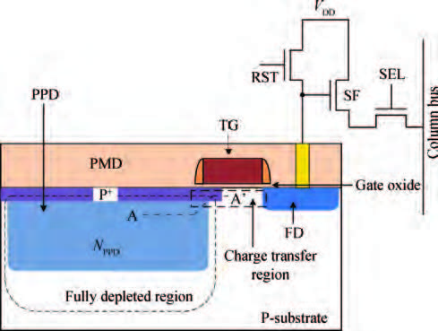
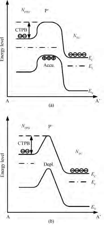
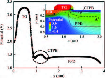
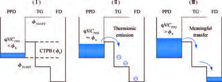
图1.
(Color online) Schematic cross-sectional diagram of the PPD and the TG in 4T-pixel.
SEMICONDUCTOR DEVICES
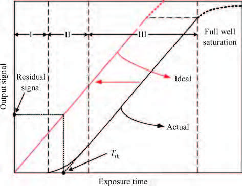
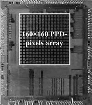
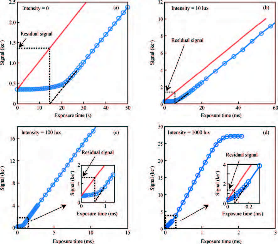
Abstract: The charge transfer potential barrier (CTPB) formed beneath the transfer gate causes a noticeable image lag issue in pinned photodiode (PPD) CMOS image sensors (CIS), and is difficult to measure straightforwardly since it is embedded inside the device. From an understanding of the CTPB formation mechanism, we report on an alternative method to feasibly measure the CTPB height by performing a linear extrapolation coupled with a horizontal left-shift on the sensor photoresponse curve under the steady-state illumination. The theoretical study was performed in detail on the principle of the proposed method. Application of the measurements on a prototype PPD-CIS chip with an array of 160 × 160 pixels is demonstrated. Such a method intends to shine new light on the guidance for the lag-free and high-speed sensors optimization based on PPD devices.
Keywords: CMOS image sensors (CIS), pinned photodiode (PPD), charge transfer potential barrier (CTPB), photoresponse curve
| [1] | |
| [2] | |
| [3] | |
| [4] | |
| [5] | |
| [6] | |
| [7] | |
| [8] | |
| [9] | |
| [10] | |
| [11] | |
| [12] | |
| [13] | |
| [14] | |
| [15] | |
| [16] | |
| [17] | |
| [18] |
| [1] | |
| [2] | |
| [3] | |
| [4] | |
| [5] | |
| [6] | |
| [7] | |
| [8] | |
| [9] | |
| [10] | |
| [11] | |
| [12] | |
| [13] | |
| [14] | |
| [15] | |
| [16] | |
| [17] | |
| [18] |


Article views: 4396 Times PDF downloads: 122 Times Cited by: 0 Times
Received: 11 September 2015 Revised: Online: Published: 01 May 2016
| Citation: |
Chen Cao, Bing Zhang, Junfeng Wang, Longsheng Wu. Measurement of charge transfer potential barrier in pinned photodiode CMOSimage sensors[J]. Journal of Semiconductors, 2016, 37(5): 054007. doi: 10.1088/1674-4926/37/5/054007
****
C Cao, B Zhang, J F Wang, L S Wu. Measurement of charge transfer potential barrier in pinned photodiode CMOSimage sensors[J]. J. Semicond., 2016, 37(5): 054007. doi: 10.1088/1674-4926/37/5/054007.

|
| [1] | |
| [2] | |
| [3] | |
| [4] | |
| [5] | |
| [6] | |
| [7] | |
| [8] | |
| [9] | |
| [10] | |
| [11] | |
| [12] | |
| [13] | |
| [14] | |
| [15] | |
| [16] | |
| [17] | |
| [18] |

 WeChat ID
Journal of Semiconductors © 2017 All Rights Reserved 京ICP备05085259号-2

 DownLoad:

