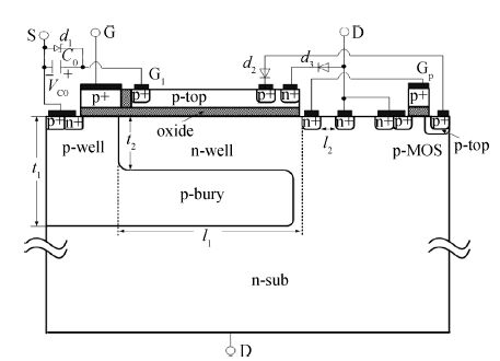
Fig1.
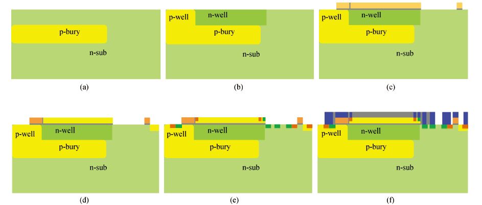
Schematic diagram of the proposed structure.
SEMICONDUCTOR DEVICES
Wenfang Du, Xinjiang Lyu and Xingbi Chen
Corresponding author: Corresponding author. Email: xbchen@uestc.edu.cn
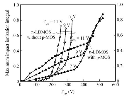
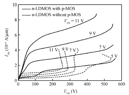
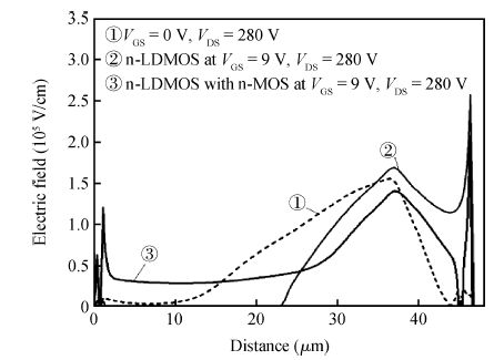
Abstract: An LDMOS with nearly rectangular-shape safe operation area (SOA) and low specific on-resistance is proposed. By utilizing a split gate, an electron accumulation layer is formed near the surface of the n-drift region to improve current conduction capability during on-state operation. As a result, the specific on-resistance can be lowered down to 74.7 mΩ·cm2 for a 600 V device from simulation. Furthermore, under high-voltage and high-current conditions, electrons and holes flow as majority carriers in the n-drift region and p-type split gate, respectively. Due to charge compensation occurring between holes and electrons, the local electric field is reduced and impact ionization is weakened in the proposed device. Therefore, a higher on-state breakdown voltage at large VGS is obtained and snap-back is suppressed as well.
Keywords: LDMOS, safe operation area (SOA), snap-back, split gate
| [1] | |
| [2] | |
| [3] | |
| [4] | |
| [5] | |
| [6] | |
| [7] | |
| [8] | |
| [9] | |
| [10] | |
| [11] | |
| [12] | |
| [13] | |
| [14] | |
| [15] | |
| [16] |
| [1] | |
| [2] | |
| [3] | |
| [4] | |
| [5] | |
| [6] | |
| [7] | |
| [8] | |
| [9] | |
| [10] | |
| [11] | |
| [12] | |
| [13] | |
| [14] | |
| [15] | |
| [16] |


Article views: 4870 Times PDF downloads: 104 Times Cited by: 0 Times
Received: 07 September 2015 Revised: Online: Published: 01 May 2016
| Citation: |
Wenfang Du, Xinjiang Lyu, Xingbi Chen. An LDMOS with large SOA and low specific on-resistance[J]. Journal of Semiconductors, 2016, 37(5): 054006. doi: 10.1088/1674-4926/37/5/054006
****
W F Du, X Lyu, X B Chen. An LDMOS with large SOA and low specific on-resistance[J]. J. Semicond., 2016, 37(5): 054006. doi: 10.1088/1674-4926/37/5/054006.

|
| [1] | |
| [2] | |
| [3] | |
| [4] | |
| [5] | |
| [6] | |
| [7] | |
| [8] | |
| [9] | |
| [10] | |
| [11] | |
| [12] | |
| [13] | |
| [14] | |
| [15] | |
| [16] |

 WeChat ID
Journal of Semiconductors © 2017 All Rights Reserved 京ICP备05085259号-2

 DownLoad: