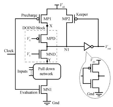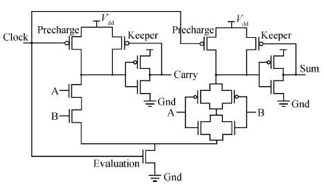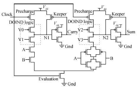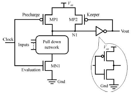
Fig. 1.
Standard domino logic circuit.
SEMICONDUCTOR INTEGRATED CIRCUITS
Ambika Prasad Shah1, Vaibhav Neema1 and Shreeniwas Daulatabad2
Corresponding author: Corresponding author. Email: ambika_shah@rediffmail.com
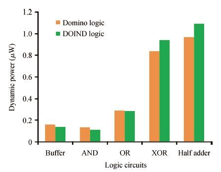
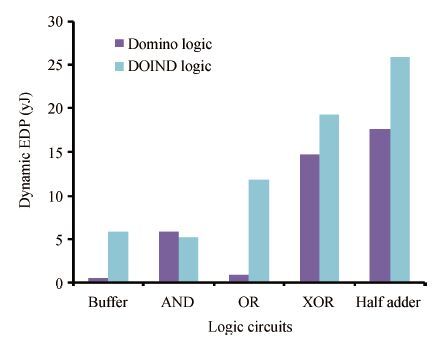
Abstract: A novel DOIND logic approach is proposed for domino logic, which reduces the leakage current with a minimum delay penalty. Simulation is performed at 70 nm technology node with supply voltage 1V for domino logic and DOIND logic based AND, OR, XOR and Half Adder circuits using the tanner EDA tool. Simulation results show that the proposed DOIND approach decreases the average leakage current by 68.83%, 66.6%, 77.86% and 74.34% for 2 input AND, OR, XOR and Half Adder respectively. The proposed approach also has 47.76% improvement in PDAP for the buffer circuit as compared to domino logic.
Keywords: deep submicron, DOIND logic, domino logic, evaluation, precharge, subthreshold leakage
| [1] | |
| [2] | |
| [3] | |
| [4] | |
| [5] | |
| [6] | |
| [7] | |
| [8] | |
| [9] | |
| [10] | |
| [11] | |
| [12] | |
| [13] | |
| [14] | |
| [15] | |
| [16] | |
| [17] | |
| [18] |
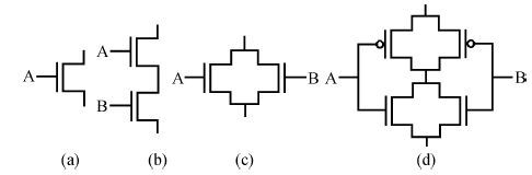
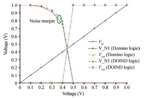
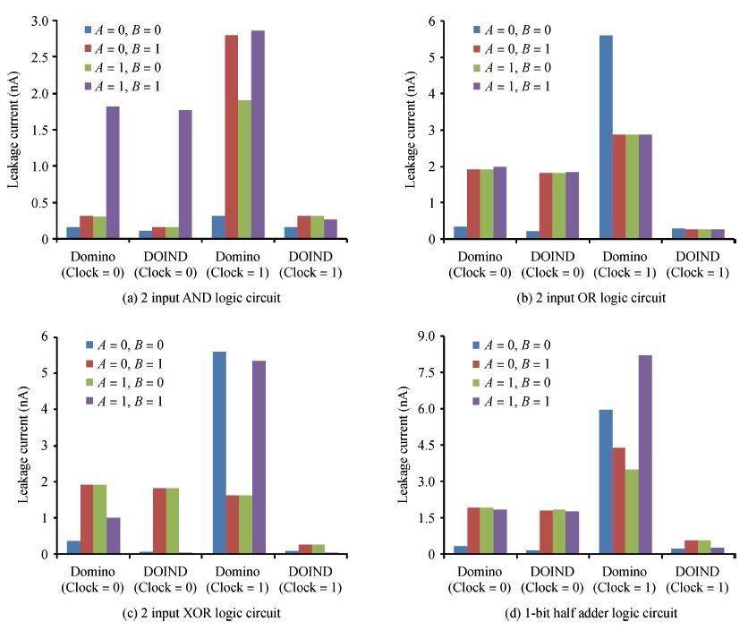
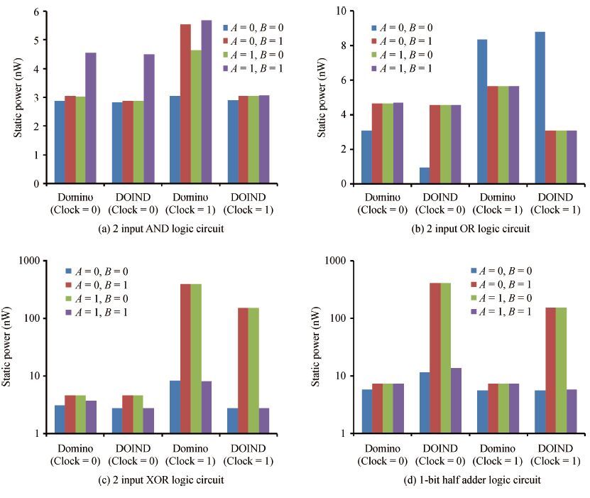
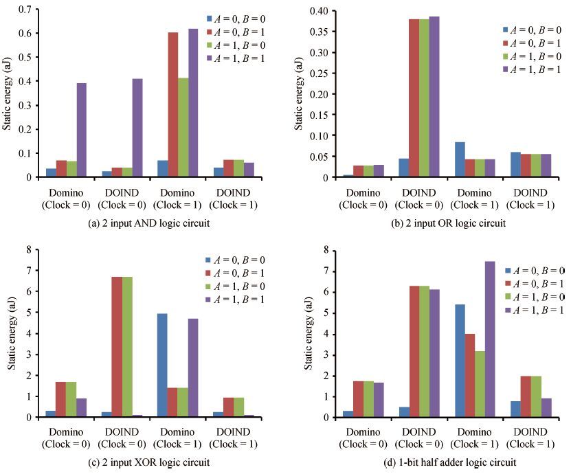
Table 3. Average improvement of Static Parameters for different combinational logic circuits.
 DownLoad: CSV
| [1] | |
| [2] | |
| [3] | |
| [4] | |
| [5] | |
| [6] | |
| [7] | |
| [8] | |
| [9] | |
| [10] | |
| [11] | |
| [12] | |
| [13] | |
| [14] | |
| [15] | |
| [16] | |
| [17] | |
| [18] |


Article views: 4151 Times PDF downloads: 25 Times Cited by: 0 Times
Received: 19 August 2015 Revised: Online: Published: 01 May 2016
| Citation: |
Ambika Prasad Shah, Vaibhav Neema, Shreeniwas Daulatabad. DOIND: a technique for leakage reduction in nanoscale domino logic circuits[J]. Journal of Semiconductors, 2016, 37(5): 055001. doi: 10.1088/1674-4926/37/5/055001
****
A P Shah, V Neema, S Daulatabad. DOIND: a technique for leakage reduction in nanoscale domino logic circuits[J]. J. Semicond., 2016, 37(5): 055001. doi: 10.1088/1674-4926/37/5/055001.

|
| [1] | |
| [2] | |
| [3] | |
| [4] | |
| [5] | |
| [6] | |
| [7] | |
| [8] | |
| [9] | |
| [10] | |
| [11] | |
| [12] | |
| [13] | |
| [14] | |
| [15] | |
| [16] | |
| [17] | |
| [18] |

 WeChat ID
Journal of Semiconductors © 2017 All Rights Reserved 京ICP备05085259号-2