| [1] |
Faria B, Silvestre N, Canongia Lopes J N. Induced anisotropy of chiral carbon nanotubes under combined tension-twisting. Mechanics of Materials, 2013, 58:97
|
| [2] |
Tada K, Yasuda M, Mitsueda T, et al. Molecular dynamics study of electron irradiation effects on mechanical properties of carbon nanotubes. Microelectron Eng, 2013, 107:50
|
| [3] |
Jeong B W, Lim J K, Sinnott S B. Torsional stiffening of carbon nanotube systems. Appl Phys Lett, 2007, 90:023102
|
| [4] |
Wu M H, Li X, Pan D, et al. Synthesis of nitrogen-doped single-walled carbon nanotubes and monitoring of doping by Raman spectroscopy. Chin Phys B, 2013, 22:086101
|
| [5] |
Karimov Kh S, Sulaiman K, Ahmad Z, et al. Novel pressure and displacement sensors based on carbon nanotubes. Chin Phys B, 2015, 24:018801
|
| [6] |
Zhang G X, Wang H H, Chen Y F, et al. Numerical simulations on effcet of Stone-Wales defects on mechanical properties of SWCNTs under axial stretch or twist loads. Journal of East China University of Science and Technology (Natural Science Edition), 2013, 01:8(in Chinese)
|
| [7] |
Zhang X W, Zhang K W. Use the molecular kynamics simulate the stability of single-walled carbon nanotube with vacancy defects. Journal of Jiangnan University (Natural Science Edition), 2011, 02:249(in Chinese)
|
| [8] |
Sharma A, Chandra R, Kumar P, et al. Effect of Stone-Wales and vacancy defects on elastic moduli of carbon nanotubes and their composites using molecular dynamics simulation. Computational Materials Science, 2014, 86:01
|
| [9] |
Partovi-Azar P, Jand S P, Namiranian A, et al. Electronic features induced by Stone-Wales defects in zigzag and chiral carbon nanotubes. Computational Materials Science, 2013, 79:82
|
| [10] |
Qing X Z, Chao Y W, Zhi B F, et al. Effects of various defects on the electronic properties of single-walled carbon nanotubes:a first principle study. Frontiers of Physics, 2014, 09:200
|
| [11] |
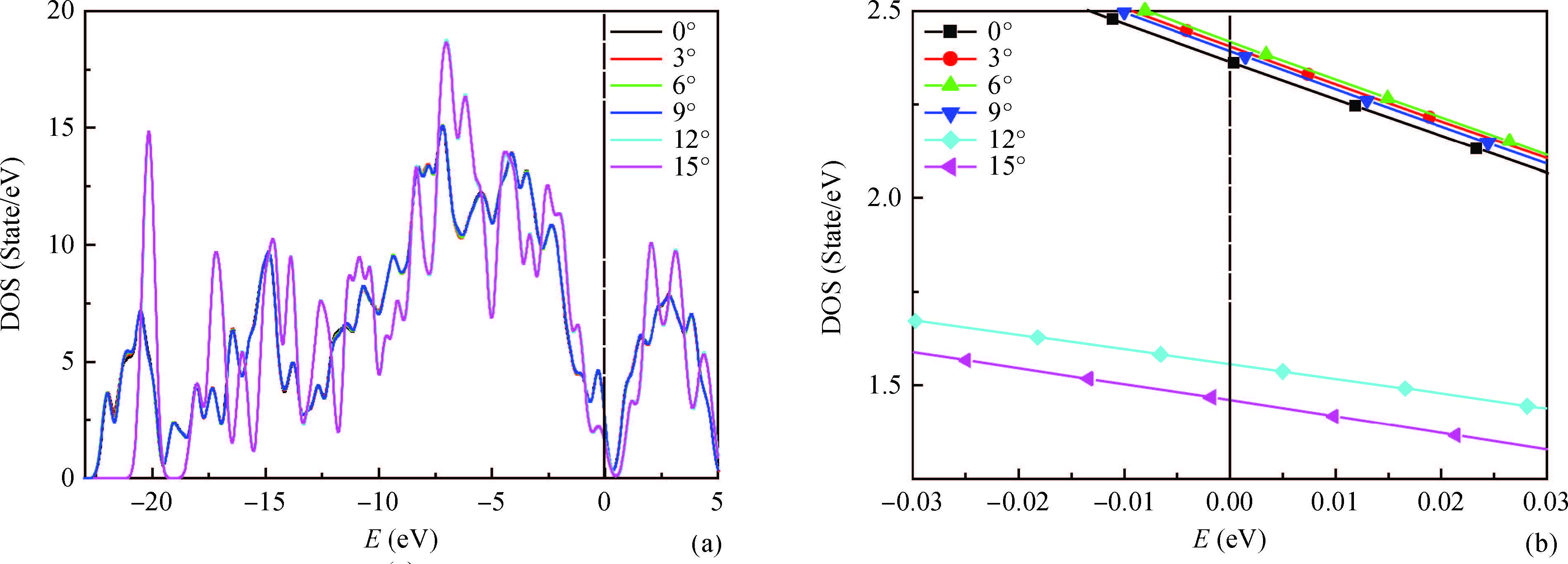
Xie Y, Luo Y, Liu S J. The effects of the uniaxial pressure on electronic structures of the (6,6) single-walled carbon nanotube crysta. Acta Physica Sinica, 2008, 57:4364(in Chinese)
|
| [12] |
Jin L, Fu H G, Xie Y, et al, Field emission properties of capped carbon nanotubes doped by alkali metals:a theoretical investigation. Chin Phys B, 2012, 05:651
|
| [13] |
Yu Z Q, Zhang C H, Li S D, et al. Electronic structures and optoelectronic properties of C/Ge-doped silicon nanotubes. Journal of Inorganic Materials, 2015, 03:233(in Chinese)
|
| [14] |
Marlo M, Milman V. Density-functional study of bulk and surface properties of titanium nitride using different exchange-correlation functionals. Phys Rev B, 2000, 62:2899
|
| [15] |
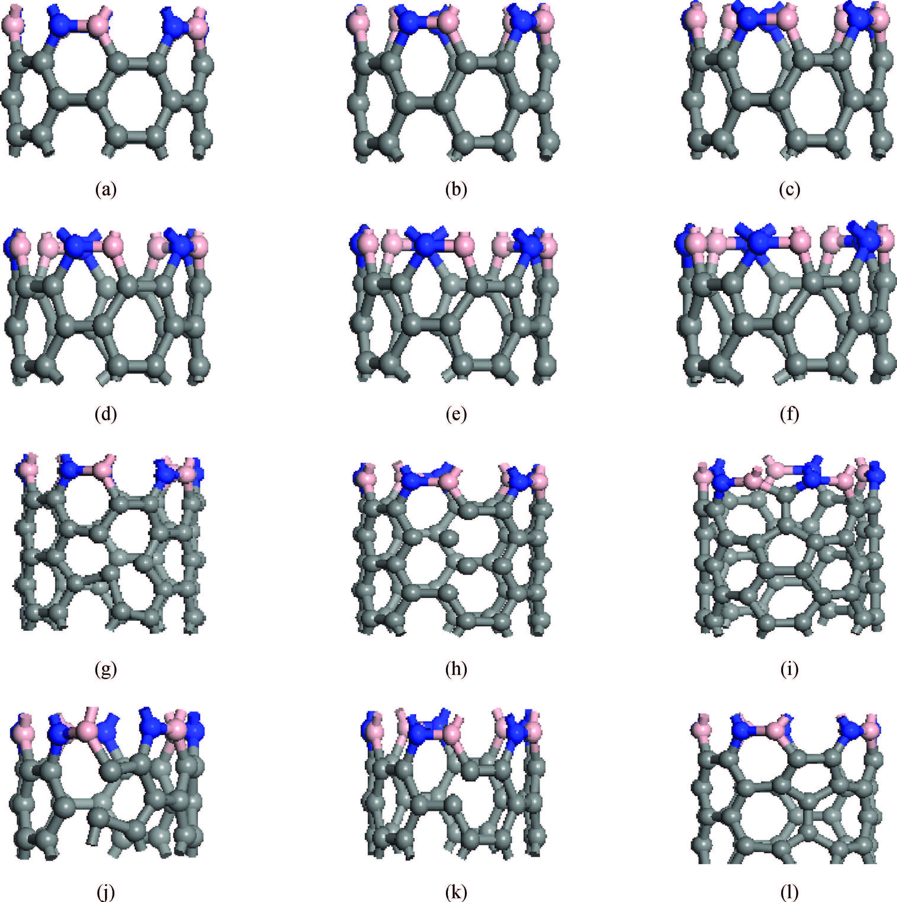
Jiang Y, Liu G L. Infuences of shear deformation on electronic structure and optical properties of B, N doped carbon nanotube superlattices. Acta Physica Sinica, 2015, 64(14):1(in Chinese)
|


 DownLoad: