


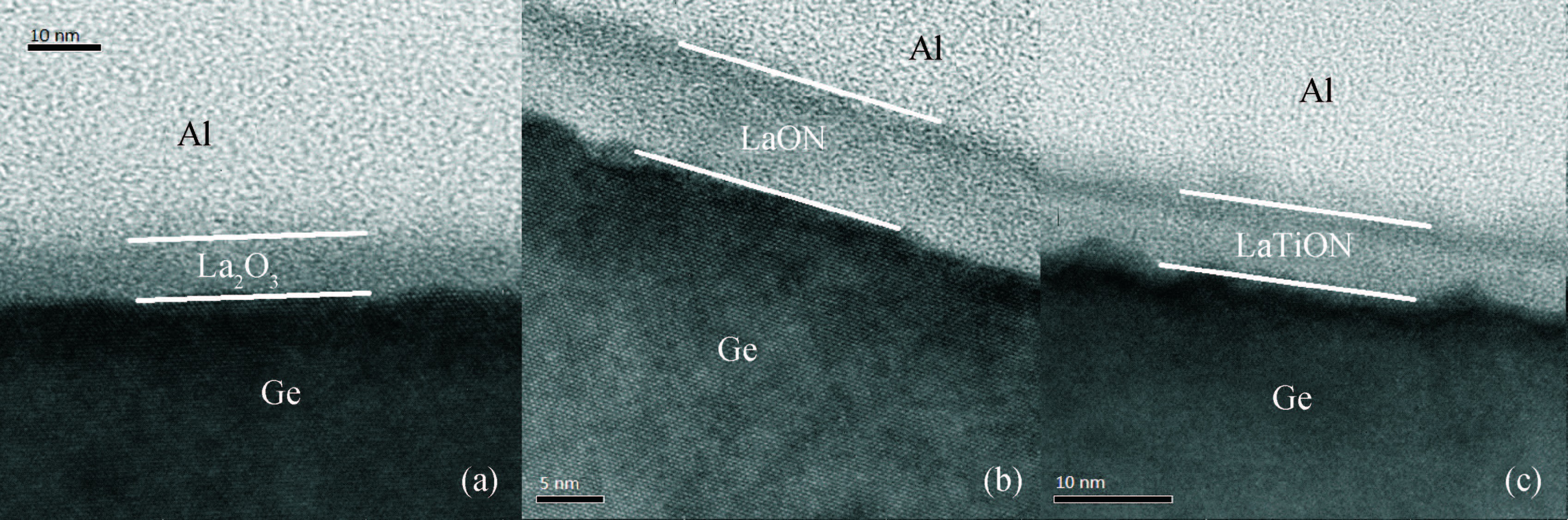
Fig. 1.
TEM pictures of (a) La2O3/Ge MOS, (b) LaON/Ge MOS and (c) LaTiON/Ge MOS.
SEMICONDUCTOR DEVICES
Huoxi Xu1 and Jingping Xu2,
Corresponding author: Jingping Xu, Email: 799904108@qq.com
Abstract: LaON, LaTiO and LaTiON films are deposited as gate dielectrics by incorporating N or/and Ti into La2O3 using the sputtering method to fabricate Ge MOS capacitors, and the electrical properties of the devices are carefully examined. LaON/Ge capacitors exhibit the best interface quality, gate leakage property and device reliability, but a smaller k value (14.9). LaTiO/Ge capacitors exhibit a higher k value (22.7), but a deteriorated interface quality, gate leakage property and device reliability. LaTiON/Ge capacitors exhibit the highest k value (24.6), and a relatively better interface quality (3.1×10¹¹ eV-1cm-2), gate leakage property (3.6×10⁻³ A/cm2 at Vg=1 V+Vfb) and device reliability. Therefore, LaTiON is more suitable for high performance Ge MOS devices as a gate dielectric than LaON and LaTiO materials.
Keywords: Ge MOS capacitor, La2O3, N or/and Ti incorporation, interface properties, k value
| [1] |
Robertson J, Wallace R M. High-k materials and metal gates for CMOS applications. Mater Sci Eng R, 2015, 88:1
|
| [2] |
Oh I K, Kim M K, Lee J S, et al. The effect of La2O3-incorporation in HfO2 dielectrics on Ge substrate by atomic layer deposition. Appl Surf Sci, 2013, 287:349
|
| [3] |
Liu Chen, Zhang Yuming, Zhang Yimen, et al. Temperature dependent interfacial and electrical characteristics during atomic layer deposition and annealing of HfO2 films in p-GaAs metal-oxide-semiconductor capacitors. Journal of Semiconductors, 2015, 36:124003
|
| [4] |
Bethge O, Henkel C, Abermann S, et al. Stability of La2O3 and GeO2 passivated Ge surfaces during ALD of ZrO2 high-k dielectric. Appl Surf Sci, 2012, 258:3444
|
| [5] |
Bom N M, Soares G V, Krug C, et al. Evolution of the Al2O3/Ge (100) interface for reactively sputter-deposited films submitted to postdeposition anneals. Appl Surf Sci, 2012, 258:5707
|
| [6] |
Zhou Jiahui, Chang Hudong, Liu Honggang, et al. MIM capacitors with various Al2O3 thicknesses for GaAs RFIC application. Journal of Semiconductors, 2015, 36:054004
|
| [7] |
Xie Q, Deduytsche D, Schaekers M, et al. Implementing TiO2 as gate dielectric for Ge-channel complementary metal-oxide-semiconductor devices by using HfO2/GeO2 interlayer. Appl Phys Lett, 2010, 97:112905
|
| [8] |
Fu C H, Chang-Liao K S, Liu L J, et al. An ultralow EOT Ge MOS device with tetragonal HfO2 and high quality HfxGeyO interfacial layer. IEEE Trans Electron Devices, 2014, 61:2662
|
| [9] |
Sun Q Q, Shi Y, Dong L, et al. Impact of germanium related defects on electrical performance of hafnium oxide. Appl Phys Lett, 2008, 92:102908
|
| [10] |
Mirovic I Z, Althobaiti M, Weerakkody A, et al. Ge interface engineering using ultra-thin La2O3 and Y2O3 films:a study into the effect of deposition temperature. J Appl Phys, 2014, 115:114102
|
| [11] |
Lamagna L, Wiemer C, Perego M, et al. O3-based atomic layer deposition of hexagonal La2O3 films on Si (100) and Ge (100) substrates. J Appl Phys, 2010, 108:084108
|
| [12] |
Galata S F, Mavrou G, Tsipas P, et al. Metal-oxide-semiconductor devices on p-type Ge with La2O3 and ZrO2/La2O3 as gate dielectric and the effect of postmetallization anneal. J Vac Sci Technol B, 2009, 27:246
|
| [13] |
Xu H X, Xu J P, Li C X, et al. Impacts of Ti on electrical properties of Ge metal-oxide-semiconductor capacitors with ultrathin high-k LaTiON gate dielectric. Appl Phys A, 2010, 99:903
|
| [14] |
Cheng C L, Horng J H, Wu Y Z. Electrical and reliability characteristics of HfLaTiO-gated metal-oxide-semiconductor capacitors with various Ti concentrations. Device Mater Reliab, 2012, 12:399
|
| [15] |
Li C X, Zou X, Lai P T, et al. Effects of Ti content and wet-N2 anneal on Ge MOS capacitors with HfTiO gate dielectric. Microelectron Reliab, 2008, 48:526
|
| [16] |
He G, Sun Z Q, Liu M, et al. Nitrogen dependence of band alignment and electrical properties of HfTiON gate dielectrics metal-oxide-semiconductor capacitor. Appl Phys Lett, 2010, 97:192902
|
| [17] |
Kawada N, Ito M, Saito Y. Thermal stability of lanthanum oxynitride ultrathin films deposited on silicon substrates. Jpn J Appl Phys, 2006, 45:9197
|
| [18] |
He G, Liu J W, Chen H S, et al. Interface control and modification of band alignment and electrical properties of HfTiO/GaAs gate stacks by nitrogen incorporation. J Mater Chem C, 2014, 2:5299
|
| [19] |
Terman L M. An investigation of surface states at a silicon/silicon oxide interface employing metal-oxide-silicon diodes. Solid State Electron, 1962, 5:285
|
| [20] |
Ji F, Xu J P, Lai P T, et al. Improved interfacial properties of Ge MOS capacitor with high-k dielectric by using TaON/GeON dual interlayer. Electron Device Lett, 2011, 32:122
|
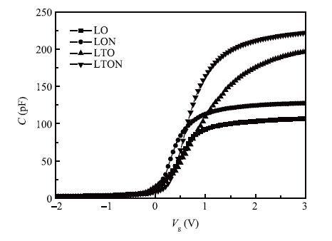
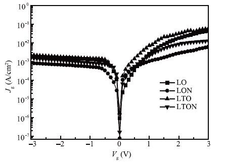
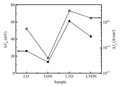
Table 1. Parameters of the Ge MOS capacitors extracted from HF (1-MHz) C-V curves, and tox is the physical thickness of gate dielectric measured by ellipsometry.
| Sample | tox (nm) | Cox (pF) | CET (nm) | Vfb (V) | Qox (cm-2) | Dit (eV-1cm-2) | k |
| LO | 7.51 | 108 | 2.5 | 0.23 | -1.03×10¹² | 3.3×10¹¹ | 11.7 |
| LON | 8.05 | 129 | 2.1 | 0.19 | -8.5×10¹¹ | 1.2×10¹¹ | 14.9 |
| LTO | 7.54 | 209 | 1.3 | 0.47 | -6.15×10¹² | 7.1×10¹¹ | 22.7 |
| LTON | 7.55 | 227 | 1.2 | 0.34 | -4.3×10¹² | 3.1×10¹¹ | 24.6 |
 DownLoad: CSV
| [1] |
Robertson J, Wallace R M. High-k materials and metal gates for CMOS applications. Mater Sci Eng R, 2015, 88:1
|
| [2] |
Oh I K, Kim M K, Lee J S, et al. The effect of La2O3-incorporation in HfO2 dielectrics on Ge substrate by atomic layer deposition. Appl Surf Sci, 2013, 287:349
|
| [3] |
Liu Chen, Zhang Yuming, Zhang Yimen, et al. Temperature dependent interfacial and electrical characteristics during atomic layer deposition and annealing of HfO2 films in p-GaAs metal-oxide-semiconductor capacitors. Journal of Semiconductors, 2015, 36:124003
|
| [4] |
Bethge O, Henkel C, Abermann S, et al. Stability of La2O3 and GeO2 passivated Ge surfaces during ALD of ZrO2 high-k dielectric. Appl Surf Sci, 2012, 258:3444
|
| [5] |
Bom N M, Soares G V, Krug C, et al. Evolution of the Al2O3/Ge (100) interface for reactively sputter-deposited films submitted to postdeposition anneals. Appl Surf Sci, 2012, 258:5707
|
| [6] |
Zhou Jiahui, Chang Hudong, Liu Honggang, et al. MIM capacitors with various Al2O3 thicknesses for GaAs RFIC application. Journal of Semiconductors, 2015, 36:054004
|
| [7] |
Xie Q, Deduytsche D, Schaekers M, et al. Implementing TiO2 as gate dielectric for Ge-channel complementary metal-oxide-semiconductor devices by using HfO2/GeO2 interlayer. Appl Phys Lett, 2010, 97:112905
|
| [8] |
Fu C H, Chang-Liao K S, Liu L J, et al. An ultralow EOT Ge MOS device with tetragonal HfO2 and high quality HfxGeyO interfacial layer. IEEE Trans Electron Devices, 2014, 61:2662
|
| [9] |
Sun Q Q, Shi Y, Dong L, et al. Impact of germanium related defects on electrical performance of hafnium oxide. Appl Phys Lett, 2008, 92:102908
|
| [10] |
Mirovic I Z, Althobaiti M, Weerakkody A, et al. Ge interface engineering using ultra-thin La2O3 and Y2O3 films:a study into the effect of deposition temperature. J Appl Phys, 2014, 115:114102
|
| [11] |
Lamagna L, Wiemer C, Perego M, et al. O3-based atomic layer deposition of hexagonal La2O3 films on Si (100) and Ge (100) substrates. J Appl Phys, 2010, 108:084108
|
| [12] |
Galata S F, Mavrou G, Tsipas P, et al. Metal-oxide-semiconductor devices on p-type Ge with La2O3 and ZrO2/La2O3 as gate dielectric and the effect of postmetallization anneal. J Vac Sci Technol B, 2009, 27:246
|
| [13] |
Xu H X, Xu J P, Li C X, et al. Impacts of Ti on electrical properties of Ge metal-oxide-semiconductor capacitors with ultrathin high-k LaTiON gate dielectric. Appl Phys A, 2010, 99:903
|
| [14] |
Cheng C L, Horng J H, Wu Y Z. Electrical and reliability characteristics of HfLaTiO-gated metal-oxide-semiconductor capacitors with various Ti concentrations. Device Mater Reliab, 2012, 12:399
|
| [15] |
Li C X, Zou X, Lai P T, et al. Effects of Ti content and wet-N2 anneal on Ge MOS capacitors with HfTiO gate dielectric. Microelectron Reliab, 2008, 48:526
|
| [16] |
He G, Sun Z Q, Liu M, et al. Nitrogen dependence of band alignment and electrical properties of HfTiON gate dielectrics metal-oxide-semiconductor capacitor. Appl Phys Lett, 2010, 97:192902
|
| [17] |
Kawada N, Ito M, Saito Y. Thermal stability of lanthanum oxynitride ultrathin films deposited on silicon substrates. Jpn J Appl Phys, 2006, 45:9197
|
| [18] |
He G, Liu J W, Chen H S, et al. Interface control and modification of band alignment and electrical properties of HfTiO/GaAs gate stacks by nitrogen incorporation. J Mater Chem C, 2014, 2:5299
|
| [19] |
Terman L M. An investigation of surface states at a silicon/silicon oxide interface employing metal-oxide-silicon diodes. Solid State Electron, 1962, 5:285
|
| [20] |
Ji F, Xu J P, Lai P T, et al. Improved interfacial properties of Ge MOS capacitor with high-k dielectric by using TaON/GeON dual interlayer. Electron Device Lett, 2011, 32:122
|


Article views: 3503 Times PDF downloads: 14 Times Cited by: 0 Times
Received: 23 November 2015 Revised: 23 February 2016 Online: Published: 01 June 2016
| Citation: |
Huoxi Xu, Jingping Xu. Electrical properties of Ge metal-oxide-semiconductor capacitors with high-k La2O3 gate dielectric incorporated by N or/and Ti[J]. Journal of Semiconductors, 2016, 37(6): 064006. doi: 10.1088/1674-4926/37/6/064006
****
H X Xu, J P Xu. Electrical properties of Ge metal-oxide-semiconductor capacitors with high-k La2O3 gate dielectric incorporated by N or/and Ti[J]. J. Semicond., 2016, 37(6): 064006. doi: 10.1088/1674-4926/37/6/064006.

|
| [1] |
Robertson J, Wallace R M. High-k materials and metal gates for CMOS applications. Mater Sci Eng R, 2015, 88:1
|
| [2] |
Oh I K, Kim M K, Lee J S, et al. The effect of La2O3-incorporation in HfO2 dielectrics on Ge substrate by atomic layer deposition. Appl Surf Sci, 2013, 287:349
|
| [3] |
Liu Chen, Zhang Yuming, Zhang Yimen, et al. Temperature dependent interfacial and electrical characteristics during atomic layer deposition and annealing of HfO2 films in p-GaAs metal-oxide-semiconductor capacitors. Journal of Semiconductors, 2015, 36:124003
|
| [4] |
Bethge O, Henkel C, Abermann S, et al. Stability of La2O3 and GeO2 passivated Ge surfaces during ALD of ZrO2 high-k dielectric. Appl Surf Sci, 2012, 258:3444
|
| [5] |
Bom N M, Soares G V, Krug C, et al. Evolution of the Al2O3/Ge (100) interface for reactively sputter-deposited films submitted to postdeposition anneals. Appl Surf Sci, 2012, 258:5707
|
| [6] |
Zhou Jiahui, Chang Hudong, Liu Honggang, et al. MIM capacitors with various Al2O3 thicknesses for GaAs RFIC application. Journal of Semiconductors, 2015, 36:054004
|
| [7] |
Xie Q, Deduytsche D, Schaekers M, et al. Implementing TiO2 as gate dielectric for Ge-channel complementary metal-oxide-semiconductor devices by using HfO2/GeO2 interlayer. Appl Phys Lett, 2010, 97:112905
|
| [8] |
Fu C H, Chang-Liao K S, Liu L J, et al. An ultralow EOT Ge MOS device with tetragonal HfO2 and high quality HfxGeyO interfacial layer. IEEE Trans Electron Devices, 2014, 61:2662
|
| [9] |
Sun Q Q, Shi Y, Dong L, et al. Impact of germanium related defects on electrical performance of hafnium oxide. Appl Phys Lett, 2008, 92:102908
|
| [10] |
Mirovic I Z, Althobaiti M, Weerakkody A, et al. Ge interface engineering using ultra-thin La2O3 and Y2O3 films:a study into the effect of deposition temperature. J Appl Phys, 2014, 115:114102
|
| [11] |
Lamagna L, Wiemer C, Perego M, et al. O3-based atomic layer deposition of hexagonal La2O3 films on Si (100) and Ge (100) substrates. J Appl Phys, 2010, 108:084108
|
| [12] |
Galata S F, Mavrou G, Tsipas P, et al. Metal-oxide-semiconductor devices on p-type Ge with La2O3 and ZrO2/La2O3 as gate dielectric and the effect of postmetallization anneal. J Vac Sci Technol B, 2009, 27:246
|
| [13] |
Xu H X, Xu J P, Li C X, et al. Impacts of Ti on electrical properties of Ge metal-oxide-semiconductor capacitors with ultrathin high-k LaTiON gate dielectric. Appl Phys A, 2010, 99:903
|
| [14] |
Cheng C L, Horng J H, Wu Y Z. Electrical and reliability characteristics of HfLaTiO-gated metal-oxide-semiconductor capacitors with various Ti concentrations. Device Mater Reliab, 2012, 12:399
|
| [15] |
Li C X, Zou X, Lai P T, et al. Effects of Ti content and wet-N2 anneal on Ge MOS capacitors with HfTiO gate dielectric. Microelectron Reliab, 2008, 48:526
|
| [16] |
He G, Sun Z Q, Liu M, et al. Nitrogen dependence of band alignment and electrical properties of HfTiON gate dielectrics metal-oxide-semiconductor capacitor. Appl Phys Lett, 2010, 97:192902
|
| [17] |
Kawada N, Ito M, Saito Y. Thermal stability of lanthanum oxynitride ultrathin films deposited on silicon substrates. Jpn J Appl Phys, 2006, 45:9197
|
| [18] |
He G, Liu J W, Chen H S, et al. Interface control and modification of band alignment and electrical properties of HfTiO/GaAs gate stacks by nitrogen incorporation. J Mater Chem C, 2014, 2:5299
|
| [19] |
Terman L M. An investigation of surface states at a silicon/silicon oxide interface employing metal-oxide-silicon diodes. Solid State Electron, 1962, 5:285
|
| [20] |
Ji F, Xu J P, Lai P T, et al. Improved interfacial properties of Ge MOS capacitor with high-k dielectric by using TaON/GeON dual interlayer. Electron Device Lett, 2011, 32:122
|

 WeChat ID
Journal of Semiconductors © 2017 All Rights Reserved 京ICP备05085259号-2


