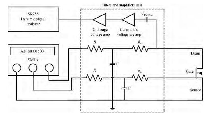
Fig. 1.
The measurement setup for low-frequency noise in the MOSFETs.
SEMICONDUCTOR DEVICES
Yuan Liu1, , Yurong Liu2, Yujuan He1, Bin Li2, Yunfei En1 and Wenxiao Fang1
Corresponding author: Yuan Liu, liuyuan@ceprei.com
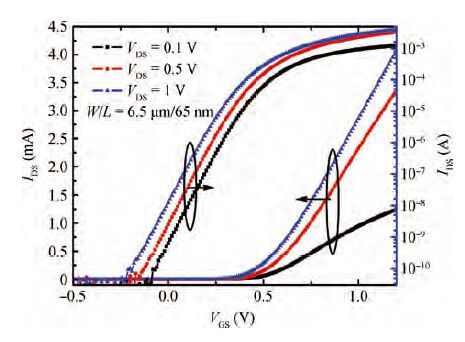
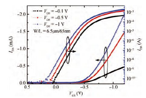
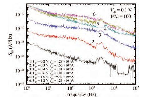
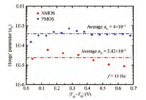
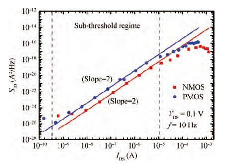
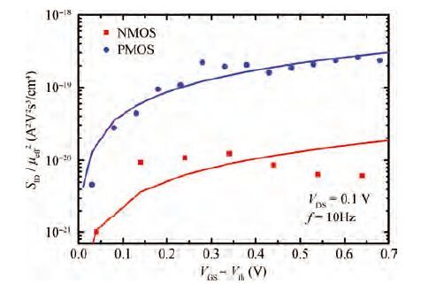
Abstract: Low-frequency noise behavior in the MOSFETs processed in 65 nm technology is investigated in this paper. Low-frequency noise for NMOS transistors agrees with McWhorter's theory (carrier number fluctuation), low-frequency noise in the sub-threshold regime agrees with McWhorter's theory for PMOS transistors while it agree with Hooge's theory (carrier mobility fluctuation) in the channel strong inversion regime. According to carrier number fluctuation model, the extracted trap densities near the interface between channel and gate oxide for NMOS and PMOS transistor are 3.94×10¹⁷ and 3.56×1018 cm-3/eV respectively. According to carrier mobility fluctuation model, the extracted average Hooge's parameters are 2.42×10⁻⁵ and 4×10⁻⁴. By consideration of BSIM compact model, it is shown that two noise parameters (NOIA and NOIB) can model the intrinsic channel noise. The extracted NOIA and NOIB are constants for PMOS and their values are equal to 3.94×1017 cm-3/eV and 9.31×10⁻⁴ V-1. But for NMOS, NOIA is also a constant while NOIB is inversely proportional to the effective gate voltage. The extracted NOIA and NOIB for NMOS are equal to 3.56×1018 cm-3/eV and 1.53×10⁻² V-1. Good agreement between simulation and experimental results is achieved.
Keywords: MOSFET, low-frequency noise, carrier number fluctuation, carrier mobility fluctuation
| [1] |
Lopez D, Haendler S, Leyris C, et al. Low-frequency noise investigation and noise variability analysis in high-k/metal gate 32-nm CMOS transistors. IEEE Trans Electron Devices, 2011, 58(8):2310
|
| [2] |
Jerng A, Sodini C G. The impact of devices type and sizing on phase noise mechanisms. IEEE J Solid-State Circuits, 2005, 40(2):360
|
| [3] |
Jones B K. Electrical noise as a reliability indicator in electronic devices and components. IEE Proceedings-Circuits Devices and Systems, 2002, 149(1):13
|
| [4] |
Ciofi C, Neri B. Low-frequency noise measurements as a characterization tool for degradation phenomena in solid-state devices. J Phys D, 2000, 33(21):R199
|
| [5] |
Liu Y, Wu W J, Li B, et al. Analysis of low-frequency noise in the amorphous indium zinc oxide thin film transistors. Acta Physica Sinica, 2014, 63(9):098503
|
| [6] |
Chen W H, Du L, Yin X S, et al. Shot noise measurement methods in electronic devices. Acta Physica Sinica, 2011, 60(10):107202
|
| [7] |
Liu Y, Wu W J, Quang L, et al. Temperature-dependent drain current characteristics and low frequency noises in indium zinc oxide thin film transistors. Chinese Physics Letters, 2015, 32(8):088506
|
| [8] |
Cozzi S A, Labate L, Stella R. Extraction of scalable electrical model for a SOI JFET using BSIM3 model. Microelectron J, 2013, 44(1):39
|
| [9] |
Ioannidis E G, Dimitriadis C A, Haendler S, et al. Improved analysis and modeling of low-frequency noise in nanoscale MOSFETs. Solid-State Electron, 2012, 76:54
|
| [10] |
Allogo Y A, de Murcia M, Vildeuil J C, et al. 1/f noise measurements in n-channel MOSFETs processed in 0.25μm technology. Solid-State Electron, 2002, 46:361
|
| [11] |
Hung K K, Ko P K, Hu C, et al. A unified model for the flicker noise in metal-oxide-semiconductor field-effect transistors. IEEE Trans Electron Devices, 1990, 37(3):654
|
| [12] |
Hung K K, Ko P K, Hu C, et al. A physics-based MOSFET noise model for circuit simulators. IEEE Trans Electron Devices, 1990, 37(5):1323
|
| [13] |
Vildeuil J C, Valenza M, Rigaud D. Extraction of the BSIM31/f noise parameters in CMOS transistors. Microelectron J, 1999, 30:199
|
| [14] |
Arora N 2007 MOSFET Modeling for VLSI Simulation:Theory and Practice (Singapore:World Scientific Publishing Co. Pte. Ltd)
|
| [15] |
Simoen E, Claeys C. On the flicker noise in submicron silicon MOSFETs. Solid-State Electron, 1999, 43(5):865
|
| [16] |
Jayaraman R, Sodini C G. A 1/f noise technique to extract the oxide trap density near the conduction band edge of silicon. IEEE Trans Electron Devices, 1989, 36(9):1773
|
| [17] |
Liu Y, Wu W J, En Y F, et al. Total dose ionizing radiation effects in the indium-zinc oxide thin-film transistors. IEEE Electron Device Lett, 2014, 35(3):369
|
| [18] |
Valenza M, Hoffmann A, Sodini D, et al. Overview of the impact of on 1/f noise in p-MOSFETs downscaling technology to 90 nm. IEE Proceedings-Circuits Devices and Systems, 2004, 151(2):102
|
| [19] |
Hooge F N. 1/f noise sources. IEEE Trans Electron Devices, 1994, 41(11):1926
|
| [20] |
Vandamme L K J, Hooge F N. What do we certainly know about 1/f noise in MOSTs. IEEE Trans Electron Devices, 2008, 55(11):3070
|
| [21] |
von Haartman M, Malm B G, Ostling M. Comprehensive study on low frequency noise and mobility in Si and SiGe pMOSFETs with high-k gate dielectrics and TiN gate. IEEE Trans Electron Devices, 2006, 53(4):836
|
| [22] |
Liu Y, Chen H B, Liu Y R, et al. Low frequency noise and radiation response in the partially depleted SOI MOSFETs with ion implanted buried oxide. Chinese Physics B, 2015, 24(8):088503
|
| [23] |
Mercha A, Pichon L, Carin R, et al. Grain boundary trap passivation in polysilicon thin film transistor investigated by low frequency noise. Thin Solid Films, 2001, 383(1/2):303
|
| [24] |
Rhayem J, Rigaud D, Valenza M, et al. 1/f noise modeling in long channel amorphous silicon thin film transistors. J Appl Phys, 2000, 87(4):1983
|
| [25] |
Vandamme L K J, Feyaerts R, Trefan G, et al. 1/f noise in pentacene and poly-thienylene vinylene thin film transistors. J Appl Phys, 2002, 91(2):719
|
| [26] |
Wang F, Celik-Butler Z. An improved physics-based 1/f noise model for deep submicron MOSFETs. Solid-State Electron, 2001, 45(2):351
|


Article views: 4223 Times PDF downloads: 72 Times Cited by: 0 Times
Received: 20 September 2015 Revised: 30 November 2015 Online: Published: 01 June 2016
| Citation: |
Yuan Liu, Yurong Liu, Yujuan He, Bin Li, Yunfei En, Wenxiao Fang. Low-frequency noise characteristics in the MOSFETs processed in 65 nm technology[J]. Journal of Semiconductors, 2016, 37(6): 064012. doi: 10.1088/1674-4926/37/6/064012
****
Y Liu, Y R Liu, Y J He, B Li, Y F En, W X Fang. Low-frequency noise characteristics in the MOSFETs processed in 65 nm technology[J]. J. Semicond., 2016, 37(6): 064012. doi: 10.1088/1674-4926/37/6/064012.

|
| [1] |
Lopez D, Haendler S, Leyris C, et al. Low-frequency noise investigation and noise variability analysis in high-k/metal gate 32-nm CMOS transistors. IEEE Trans Electron Devices, 2011, 58(8):2310
|
| [2] |
Jerng A, Sodini C G. The impact of devices type and sizing on phase noise mechanisms. IEEE J Solid-State Circuits, 2005, 40(2):360
|
| [3] |
Jones B K. Electrical noise as a reliability indicator in electronic devices and components. IEE Proceedings-Circuits Devices and Systems, 2002, 149(1):13
|
| [4] |
Ciofi C, Neri B. Low-frequency noise measurements as a characterization tool for degradation phenomena in solid-state devices. J Phys D, 2000, 33(21):R199
|
| [5] |
Liu Y, Wu W J, Li B, et al. Analysis of low-frequency noise in the amorphous indium zinc oxide thin film transistors. Acta Physica Sinica, 2014, 63(9):098503
|
| [6] |
Chen W H, Du L, Yin X S, et al. Shot noise measurement methods in electronic devices. Acta Physica Sinica, 2011, 60(10):107202
|
| [7] |
Liu Y, Wu W J, Quang L, et al. Temperature-dependent drain current characteristics and low frequency noises in indium zinc oxide thin film transistors. Chinese Physics Letters, 2015, 32(8):088506
|
| [8] |
Cozzi S A, Labate L, Stella R. Extraction of scalable electrical model for a SOI JFET using BSIM3 model. Microelectron J, 2013, 44(1):39
|
| [9] |
Ioannidis E G, Dimitriadis C A, Haendler S, et al. Improved analysis and modeling of low-frequency noise in nanoscale MOSFETs. Solid-State Electron, 2012, 76:54
|
| [10] |
Allogo Y A, de Murcia M, Vildeuil J C, et al. 1/f noise measurements in n-channel MOSFETs processed in 0.25μm technology. Solid-State Electron, 2002, 46:361
|
| [11] |
Hung K K, Ko P K, Hu C, et al. A unified model for the flicker noise in metal-oxide-semiconductor field-effect transistors. IEEE Trans Electron Devices, 1990, 37(3):654
|
| [12] |
Hung K K, Ko P K, Hu C, et al. A physics-based MOSFET noise model for circuit simulators. IEEE Trans Electron Devices, 1990, 37(5):1323
|
| [13] |
Vildeuil J C, Valenza M, Rigaud D. Extraction of the BSIM31/f noise parameters in CMOS transistors. Microelectron J, 1999, 30:199
|
| [14] |
Arora N 2007 MOSFET Modeling for VLSI Simulation:Theory and Practice (Singapore:World Scientific Publishing Co. Pte. Ltd)
|
| [15] |
Simoen E, Claeys C. On the flicker noise in submicron silicon MOSFETs. Solid-State Electron, 1999, 43(5):865
|
| [16] |
Jayaraman R, Sodini C G. A 1/f noise technique to extract the oxide trap density near the conduction band edge of silicon. IEEE Trans Electron Devices, 1989, 36(9):1773
|
| [17] |
Liu Y, Wu W J, En Y F, et al. Total dose ionizing radiation effects in the indium-zinc oxide thin-film transistors. IEEE Electron Device Lett, 2014, 35(3):369
|
| [18] |
Valenza M, Hoffmann A, Sodini D, et al. Overview of the impact of on 1/f noise in p-MOSFETs downscaling technology to 90 nm. IEE Proceedings-Circuits Devices and Systems, 2004, 151(2):102
|
| [19] |
Hooge F N. 1/f noise sources. IEEE Trans Electron Devices, 1994, 41(11):1926
|
| [20] |
Vandamme L K J, Hooge F N. What do we certainly know about 1/f noise in MOSTs. IEEE Trans Electron Devices, 2008, 55(11):3070
|
| [21] |
von Haartman M, Malm B G, Ostling M. Comprehensive study on low frequency noise and mobility in Si and SiGe pMOSFETs with high-k gate dielectrics and TiN gate. IEEE Trans Electron Devices, 2006, 53(4):836
|
| [22] |
Liu Y, Chen H B, Liu Y R, et al. Low frequency noise and radiation response in the partially depleted SOI MOSFETs with ion implanted buried oxide. Chinese Physics B, 2015, 24(8):088503
|
| [23] |
Mercha A, Pichon L, Carin R, et al. Grain boundary trap passivation in polysilicon thin film transistor investigated by low frequency noise. Thin Solid Films, 2001, 383(1/2):303
|
| [24] |
Rhayem J, Rigaud D, Valenza M, et al. 1/f noise modeling in long channel amorphous silicon thin film transistors. J Appl Phys, 2000, 87(4):1983
|
| [25] |
Vandamme L K J, Feyaerts R, Trefan G, et al. 1/f noise in pentacene and poly-thienylene vinylene thin film transistors. J Appl Phys, 2002, 91(2):719
|
| [26] |
Wang F, Celik-Butler Z. An improved physics-based 1/f noise model for deep submicron MOSFETs. Solid-State Electron, 2001, 45(2):351
|

 WeChat ID
Journal of Semiconductors © 2017 All Rights Reserved 京ICP备05085259号-2

 DownLoad: