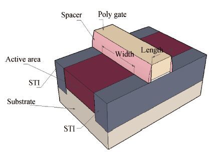
Fig. 1.
(Color online) Structure of NMOSFETs used in this work.
SEMICONDUCTOR DEVICES
Dezhao Yu1, 2, 3, Qiwen Zheng1, 2, , Jiangwei Cui1, 2, Hang Zhou1, 2, 3, Xuefeng Yu1, 2 and Qi Guo1, 2
Corresponding author: Qiwen Zheng, Email: qwzheng@ms.xjb.ac.cn
Abstract: In this paper, total dose responses and reliability issues of MOSFETs fabricated by 65 nm CMOS technology were examined. "Radiation-induced narrow channel effect" is observed in a narrow channel device. Similar to total dose responses of NMOSFETs, narrow channel NMOSFEs have larger hot-carrier-induced degradation than wide channel devices. Step Time-Dependent Dielectric Breakdown (TDDB) stresses are applied, and narrow channel devices have higher breakdown voltage than wide channel devices, which agree with "weakest link" theory of TDDB. Experimental results show that linear current, transconductance, saturated drain current and subthreshold swing are superposed degenerated by total dose irradiation and reliability issues, which may result in different lifetime from that considering total dose irradiation reliability issues separately.
Keywords: total dose responses, reliability, lifetime
| [1] |
Zhao Di, Luo Qian, Wang Xiangzhan, et al. Performance enhancement of c-CESL-strained 95-nm-gate NMOSFET using trench-based structure. Journal of Semiconductors, 2015, 36(1):014010
|
| [2] |
Ren Shangqing, Yang Hong, Tang Bo, et al. Characterization of positive bias temperature instability of NMOSFET with high-k/metal gate last process. Journal of Semiconductors, 2015, 36(1):014007
|
| [3] |
Colinge J P. Hot-electron effects in silicon-on-insulator n-channel MOSFET's. IEEE Trans Electron Devices, 1987, ED-34:2173
|
| [4] |
Wu E, Nowak E, Vayshenker A, et al. CMOS scaling beyond the 100 nm node with silicon-dioxide-based gate dielectrics. IBM J Res Develop, 2002, (46):287
|
| [5] |
Yashchin E, Li Baozhen, Stathis J, et al. Min-log approach to modeling dielectric breakdown data. IEEE International Reliability Physics Symposium (IRPS), 2012:GD.4.1
|
| [6] |
Ma Xiaohua, Hao Yue, Chen Haifeng, et al. The breakdown characteristics of ultra-thin gate oxide n-MOSFET under voltage stress. Acta Phys Sin, 2006, 55(11):6118
|
| [7] |
Cui Jiangwei. Research on radiation and reliability effects of ultra deep sub-micro CMOS device for space application. Urumqi:Xinjiang Technical Institute of Physics and Chemistry, Chinese Academy of Sciences, 2012:49
|
| [8] |
Shaneyfelt M R, Dodd P E, Draper B L, et al. Challenges in hardening technologies using shallow-trench isolation. IEEE Trans Nucl Sci, 199845(6):2584
|
| [9] |
Faccio F, Cervelli G. Radiation induced edge effects in deep submicron CMOS transistors. IEEE Trans Nucl Sci, 2005, 52:2413
|
| [10] |
Shaneyfelt M R, Schwank J R, Fleetwood D M, et al. Interfacetrap buildup rates in wet and dry oxides. IEEE Trans Nucl Sci, 1992, 39(6):2244
|
| [11] |
Lai S K. Two carrier nature of interface state generation in hole trapping and radiation damage. Appl Phys Lett, 1981, 38:58
|
| [12] |
Cui Jiangwei, Yu Xuefeng, Ren Diyuan, et al. The influence of channel size on total dose irradiation and hot carrier effects of sub-micro NMOSFET. Acta Phys Sin, 2012, 61(2):026102
|
| [13] |
Schwank J R, Shaneyfelt M R, Fleetwood D M, et al. Radiation effects in MOS oxides. IEEE Trans Nucl Sci, 2008, 55(4):1833
|
| [14] |
Silvestri M, Gerardin S, Paccagnella A, et al. Channel hot carrier stress on irradiated 130-nm NMOSFETs. IEEE Trans Nucl Sci, 2008, 56(4):1960
|
| [15] |
Silvestri M, Gerardin S, Schrimpf R D, et al. The role of irradiation bias on the time dependent dielectric breakdown of 130-nm MOSFETs exposed to X-rays. IEEE Trans Nucl Sci, 2009, 56(6):3244
|
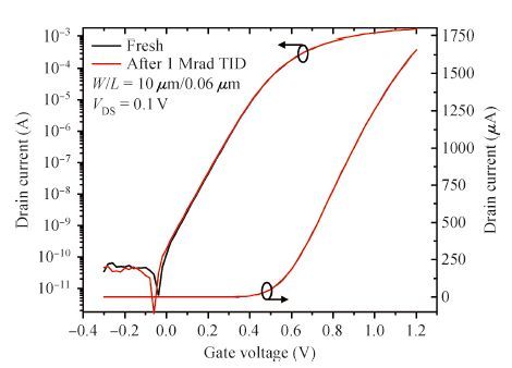
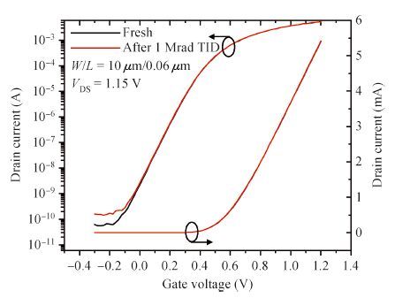
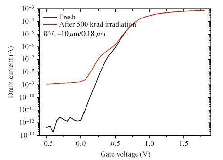
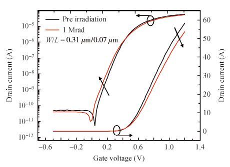
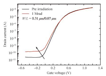
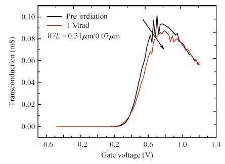
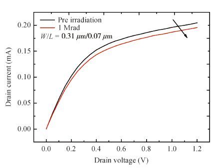
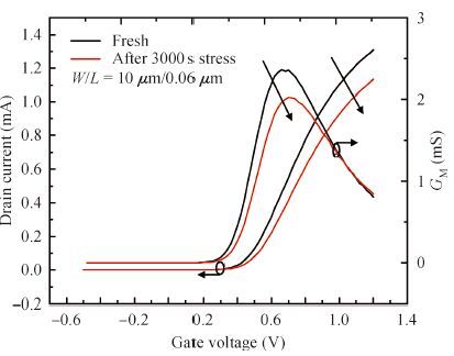
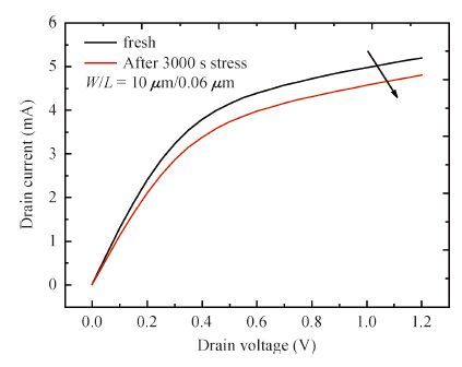
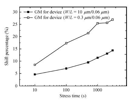
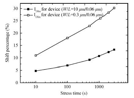
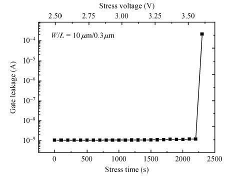
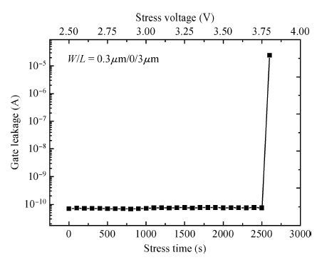
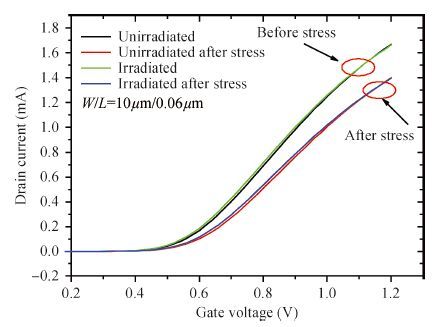
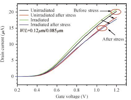
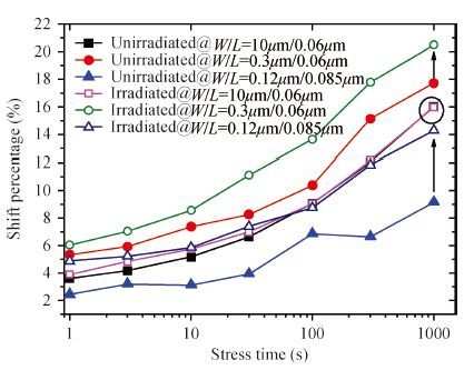
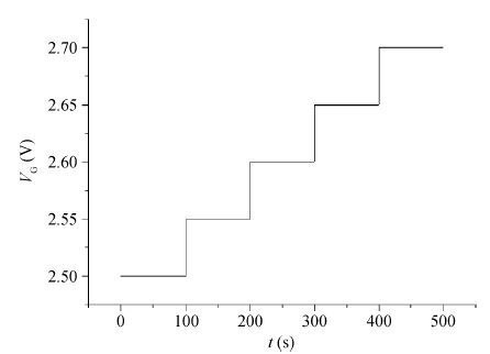
Table 1. Experimental details of total dose irradiation and reliability issues.
| Experiments | Bias | Devices (W/L, type) |
| TID | VG=1.32 V, all other pins grounded | 10 µm/0.06 µm 0.31 µm/0.07 µm |
| HCI | VD=2 V, VG= 1 V, all other pins grounded | 10 µm/0.06 µm 0.3 µm/0.06 µm 0.12 µm /0.085 µm |
| TDDB | Step Stress in Gate, start with 2.5 V, each step lasts 100 s and then increased by 0.05 V | 10 µm/0.3 µm 0.3 µm/0.3 µm |
 DownLoad: CSV
| [1] |
Zhao Di, Luo Qian, Wang Xiangzhan, et al. Performance enhancement of c-CESL-strained 95-nm-gate NMOSFET using trench-based structure. Journal of Semiconductors, 2015, 36(1):014010
|
| [2] |
Ren Shangqing, Yang Hong, Tang Bo, et al. Characterization of positive bias temperature instability of NMOSFET with high-k/metal gate last process. Journal of Semiconductors, 2015, 36(1):014007
|
| [3] |
Colinge J P. Hot-electron effects in silicon-on-insulator n-channel MOSFET's. IEEE Trans Electron Devices, 1987, ED-34:2173
|
| [4] |
Wu E, Nowak E, Vayshenker A, et al. CMOS scaling beyond the 100 nm node with silicon-dioxide-based gate dielectrics. IBM J Res Develop, 2002, (46):287
|
| [5] |
Yashchin E, Li Baozhen, Stathis J, et al. Min-log approach to modeling dielectric breakdown data. IEEE International Reliability Physics Symposium (IRPS), 2012:GD.4.1
|
| [6] |
Ma Xiaohua, Hao Yue, Chen Haifeng, et al. The breakdown characteristics of ultra-thin gate oxide n-MOSFET under voltage stress. Acta Phys Sin, 2006, 55(11):6118
|
| [7] |
Cui Jiangwei. Research on radiation and reliability effects of ultra deep sub-micro CMOS device for space application. Urumqi:Xinjiang Technical Institute of Physics and Chemistry, Chinese Academy of Sciences, 2012:49
|
| [8] |
Shaneyfelt M R, Dodd P E, Draper B L, et al. Challenges in hardening technologies using shallow-trench isolation. IEEE Trans Nucl Sci, 199845(6):2584
|
| [9] |
Faccio F, Cervelli G. Radiation induced edge effects in deep submicron CMOS transistors. IEEE Trans Nucl Sci, 2005, 52:2413
|
| [10] |
Shaneyfelt M R, Schwank J R, Fleetwood D M, et al. Interfacetrap buildup rates in wet and dry oxides. IEEE Trans Nucl Sci, 1992, 39(6):2244
|
| [11] |
Lai S K. Two carrier nature of interface state generation in hole trapping and radiation damage. Appl Phys Lett, 1981, 38:58
|
| [12] |
Cui Jiangwei, Yu Xuefeng, Ren Diyuan, et al. The influence of channel size on total dose irradiation and hot carrier effects of sub-micro NMOSFET. Acta Phys Sin, 2012, 61(2):026102
|
| [13] |
Schwank J R, Shaneyfelt M R, Fleetwood D M, et al. Radiation effects in MOS oxides. IEEE Trans Nucl Sci, 2008, 55(4):1833
|
| [14] |
Silvestri M, Gerardin S, Paccagnella A, et al. Channel hot carrier stress on irradiated 130-nm NMOSFETs. IEEE Trans Nucl Sci, 2008, 56(4):1960
|
| [15] |
Silvestri M, Gerardin S, Schrimpf R D, et al. The role of irradiation bias on the time dependent dielectric breakdown of 130-nm MOSFETs exposed to X-rays. IEEE Trans Nucl Sci, 2009, 56(6):3244
|


Article views: 3917 Times PDF downloads: 28 Times Cited by: 0 Times
Received: 04 December 2015 Revised: 23 December 2015 Online: Published: 01 June 2016
| Citation: |
Dezhao Yu, Qiwen Zheng, Jiangwei Cui, Hang Zhou, Xuefeng Yu, Qi Guo. Total dose responses and reliability issues of 65 nm NMOSFETs[J]. Journal of Semiconductors, 2016, 37(6): 064016. doi: 10.1088/1674-4926/37/6/064016
****
D Z Yu, Q W Zheng, J W Cui, H Zhou, X F Yu, Q Guo. Total dose responses and reliability issues of 65 nm NMOSFETs[J]. J. Semicond., 2016, 37(6): 064016. doi: 10.1088/1674-4926/37/6/064016.

|
| [1] |
Zhao Di, Luo Qian, Wang Xiangzhan, et al. Performance enhancement of c-CESL-strained 95-nm-gate NMOSFET using trench-based structure. Journal of Semiconductors, 2015, 36(1):014010
|
| [2] |
Ren Shangqing, Yang Hong, Tang Bo, et al. Characterization of positive bias temperature instability of NMOSFET with high-k/metal gate last process. Journal of Semiconductors, 2015, 36(1):014007
|
| [3] |
Colinge J P. Hot-electron effects in silicon-on-insulator n-channel MOSFET's. IEEE Trans Electron Devices, 1987, ED-34:2173
|
| [4] |
Wu E, Nowak E, Vayshenker A, et al. CMOS scaling beyond the 100 nm node with silicon-dioxide-based gate dielectrics. IBM J Res Develop, 2002, (46):287
|
| [5] |
Yashchin E, Li Baozhen, Stathis J, et al. Min-log approach to modeling dielectric breakdown data. IEEE International Reliability Physics Symposium (IRPS), 2012:GD.4.1
|
| [6] |
Ma Xiaohua, Hao Yue, Chen Haifeng, et al. The breakdown characteristics of ultra-thin gate oxide n-MOSFET under voltage stress. Acta Phys Sin, 2006, 55(11):6118
|
| [7] |
Cui Jiangwei. Research on radiation and reliability effects of ultra deep sub-micro CMOS device for space application. Urumqi:Xinjiang Technical Institute of Physics and Chemistry, Chinese Academy of Sciences, 2012:49
|
| [8] |
Shaneyfelt M R, Dodd P E, Draper B L, et al. Challenges in hardening technologies using shallow-trench isolation. IEEE Trans Nucl Sci, 199845(6):2584
|
| [9] |
Faccio F, Cervelli G. Radiation induced edge effects in deep submicron CMOS transistors. IEEE Trans Nucl Sci, 2005, 52:2413
|
| [10] |
Shaneyfelt M R, Schwank J R, Fleetwood D M, et al. Interfacetrap buildup rates in wet and dry oxides. IEEE Trans Nucl Sci, 1992, 39(6):2244
|
| [11] |
Lai S K. Two carrier nature of interface state generation in hole trapping and radiation damage. Appl Phys Lett, 1981, 38:58
|
| [12] |
Cui Jiangwei, Yu Xuefeng, Ren Diyuan, et al. The influence of channel size on total dose irradiation and hot carrier effects of sub-micro NMOSFET. Acta Phys Sin, 2012, 61(2):026102
|
| [13] |
Schwank J R, Shaneyfelt M R, Fleetwood D M, et al. Radiation effects in MOS oxides. IEEE Trans Nucl Sci, 2008, 55(4):1833
|
| [14] |
Silvestri M, Gerardin S, Paccagnella A, et al. Channel hot carrier stress on irradiated 130-nm NMOSFETs. IEEE Trans Nucl Sci, 2008, 56(4):1960
|
| [15] |
Silvestri M, Gerardin S, Schrimpf R D, et al. The role of irradiation bias on the time dependent dielectric breakdown of 130-nm MOSFETs exposed to X-rays. IEEE Trans Nucl Sci, 2009, 56(6):3244
|

 WeChat ID
Journal of Semiconductors © 2017 All Rights Reserved 京ICP备05085259号-2