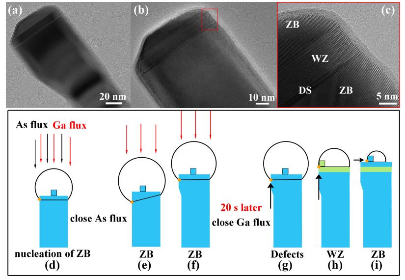
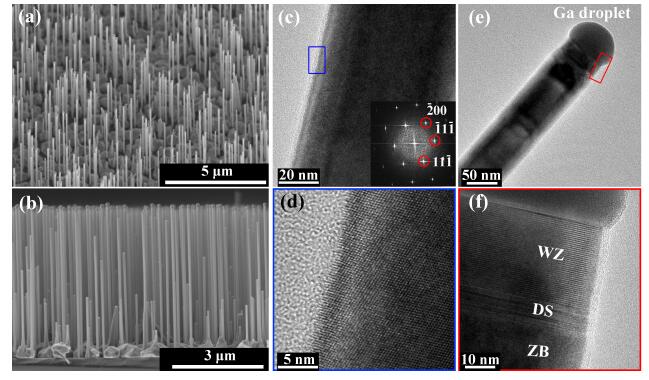
| [1] |
Borg B M, Dick K A, Ganjipour B, et al. InAs/GaSb heterostructure nanowires for tunnel field-effect transistors. Nano Lett, 2010, 10(10):4080 doi: 10.1021/nl102145h |
| [2] |
Tatebayashi J, Kako S, Ho J, et al. Room-temperature lasing in a single nanowire with quantum dots. Nat Photon, 2015, 9(8):501 doi: 10.1038/nphoton.2015.111 |
| [3] |
Pan D, Fu M, Yu X, et al. Controlled synthesis of phase-pure InAs nanowires on Si(111) by diminishing the diameter to 10 nm. Nano Lett, 2014, 14(3):1214 doi: 10.1021/nl4040847 |
| [4] |
Pan D, Fan D X, Kang N, et al. Free-standing two-dimensional single-crystalline InSb nanosheets. Nano Lett, 2016, 16(2):834 doi: 10.1021/acs.nanolett.5b04845 |
| [5] |
Li L X, Pan D, Xue Y Z, et al. Near full-composition-range highquality GaAs 1-xSb x nanowires grown by molecular-beam epitaxy. Nano Lett, 2017, 17(2):622 doi: 10.1021/acs.nanolett.6b03326 |
| [6] |
Joyce H J, Parkinson P, Jiang N, et al. Electron mobilities approaching bulk limits in "surface-free" GaAs nanowires. Nano Lett, 2014, 14(10):5989 doi: 10.1021/nl503043p |
| [7] |
Yao M, Huang N, Cong S, et al. GaAs nanowire array solar cells with axial p-i-n junctions. Nano Lett, 2014, 14(6):3293 doi: 10.1021/nl500704r |
| [8] |
Wang H. High gain single GaAs nanowire photodetector. Appl Phys Lett, 2013, 103(9):093101 doi: 10.1063/1.4816246 |
| [9] |
Tomioka K, Motohisa J, Hara S, et al. GaAs/AlGaAs core multishell nanowire-based light-emitting diodes on Si. Nano Lett, 2010, 10(5):1639 doi: 10.1021/nl9041774 |
| [10] |
Krogstrup P, Jørgensen H I, Heiss M, et al. Single-nanowire solar cells beyond the Shockley-Queisser limit. Nat Photon, 2013, 7(4):306 doi: 10.1038/nphoton.2013.32 |
| [11] |
Harmand J C, Patriarche G, Péré-Laperne N, et al. Analysis of vapor-liquid-solid mechanism in Au-assisted GaAs nanowire growth. Appl Phys Lett, 2005, 87(20):203101 doi: 10.1063/1.2128487 |
| [12] |
Wu Z H, Mei X Y, Kim D, et al. Growth of Au-catalyzed sequenceed GaAs nanowire arrays by molecular-beam epitaxy. Appl Phys Lett, 2002, 81(27):5177 doi: 10.1063/1.1532772 |
| [13] |
Persson A I, Larsson M W, Stenstrom S, et al. Solid-phase diffusion mechanism for GaAs nanowire growth. Nat Mater, 2004, 3(10):677 doi: 10.1038/nmat1220 |
| [14] |
Tchernycheva M, Harmand J C, Patriarche G, et al. Temperature conditions for GaAs nanowire formation by Au-assisted molecular beam epitaxy. Nanotechnology, 2006, 17(16):4025 doi: 10.1088/0957-4484/17/16/005 |
| [15] |
Zhao Y, Li X, Wang W, et al. Growth and properties of GaAs nanowires on fused quartz substrate. J Semicond, 2014, 35(9):093002 doi: 10.1088/1674-4926/35/9/093002 |
| [16] |
Li R, Huang H, Ren X, et al. Growth of pure zinc blende p-type GaAs nanowires by metal-organic chemical vapor deposition. J Semicond, 2011, 32(5):053003 doi: 10.1088/1674-4926/32/5/053003 |
| [17] |
Zhou C, Zheng K, Lu Z Y, et al. Quality control of GaAs nanowire structures by limiting As flux in molecular beam epitaxy. J Phys Chem C, 2015, 119, 20721 doi: 10.1021/acs.jpcc.5b05606 |
| [18] |
Paek J H, Nishiwaki T, Yamaguchi M, et al. Catalyst free MBEVLS growth of GaAs nanowires on (111) Si substrate. Phys Status Solidi C, 2009, 6(6):1436 doi: 10.1002/pssc.v6:6 |
| [19] |
Krogstrup P, Popovitz-Biro R, Johnson E, et al. Structural phase control in self-catalyzed growth of GaAs nanowires on silicon (111). Nano Lett, 2010, 10(11):4475 doi: 10.1021/nl102308k |
| [20] |
Ramdani M R, Harmand J C, Glas F, et al. Arsenic pathways in self-catalyzed growth of GaAs nanowires. Cryst Growth Des, 2013, 13(1):91 doi: 10.1021/cg301167g |
| [21] |
Spirkoska D, Arbiol J, Gustafsson A, et al. Structural and optical properties of high quality zinc-blende/wurtzite GaAs nanowire heterostructures. Phys Rev B, 2009, 80(24):245325 doi: 10.1103/PhysRevB.80.245325 |
| [22] |
Yamaguchi M, Paek J H, Amano H. Probability of twin formation on self-catalyzed GaAs nanowires on Si substrate. Nanoscale Res Lett, 2012, 7(1):558 doi: 10.1186/1556-276X-7-558 |
| [23] |
Plissard S, Dick K A, Larrieu G, et al. Gold-free growth of GaAs nanowires on silicon:arrays and polytypism. Nanotechnology, 2010, 21(38):385602 doi: 10.1088/0957-4484/21/38/385602 |
| [24] |
Yu X, Wang H, Lu J, et al. Evidence for structural phase transitions induced by the triple phase line shift in self-catalyzed GaAs nanowires. Nano Lett, 2012, 12(10):5436 doi: 10.1021/nl303323t |
| [25] |
Bauer B, Rudolph A, Soda M, et al. Position controlled selfcatalyzed growth of GaAs nanowires by molecular beam epitaxy. Nanotechnology, 2010, 21(43):435601 doi: 10.1088/0957-4484/21/43/435601 |
| [26] |
Tchernycheva M, Harmand J C, Patriarche G, et al. Temperature conditions for GaAs nanowire formation by Au-assisted molecular beam epitaxy. Nanotechnology, 2006, 17(16):4025 doi: 10.1088/0957-4484/17/16/005 |
| [27] |
Yu X, Li L, Wang H, et al. Two-step fabrication of self-catalyzed Ga-based semiconductor nanowires on Si by molecular-beam epitaxy. Nanoscale, 2016, 8(20):10615 doi: 10.1039/C5NR07830J |
| [28] |
Wang Y, Zhang X, Sun X, et al. Enhanced optical properties in inclined GaAs nanowire arrays for high-efficiency solar cells. Opt Laser Technol, 2016, 85:85 doi: 10.1016/j.optlastec.2016.05.022 |
| [29] |
Morral A F I, Colombo C, Abstreiter G, et al. Nucleation mechanism of gallium-assisted molecular beam epitaxy growth of gallium arsenide nanowires. Appl Phys Lett, 2008, 92(6):063112 doi: 10.1063/1.2837191 |
| [30] |
Wu Z H, Mei X, Kim D, et al. Growth, branching, and kinking of molecular-beam epitaxial 〈11 1〉 GaAs nanowires. Appl Phys Lett, 2003, 83(16):3368 doi: 10.1063/1.1618018 |
| [31] |
Han N, Yang Z X, Wang F, et al. Crystal Orientation controlled photovoltaic properties of multilayer GaAs nanowire arrays. ACS Nano, 2016, 10(6):6283 doi: 10.1021/acsnano.6b02473 |
| [32] |
Ren D, Dheeraj D L, Jin C, et al. New Insights into the origins of Sb-induced effects on self-catalyzed GaAsSb nanowire arrays. Nano Lett, 2016, 16(2):1201 doi: 10.1021/acs.nanolett.5b04503 |
| [33] |
Krogstrup P, Curiotto S, Johnson E, et al. Impact of the liquid phase shape on the structure of Ⅲ-V nanowires. Phys Rev Lett, 2011, 106(12):125505 doi: 10.1103/PhysRevLett.106.125505 |
| [34] |
Munshi A M, Dheeraj D L, Todorovic J, et al. Crystal phase engineering in self-catalyzed GaAs and GaAs/GaAsSb nanowires grown on Si(111). J Cryst Growth, 2013, 372:163 doi: 10.1016/j.jcrysgro.2013.03.004 |
| [35] |
Glas F, Harmand J C, Patriarche G. Why does wurtzite form in nanowires of Ⅲ-V zinc-blende semiconductors. Phys Rev Lett, 2007, 99:146101 doi: 10.1103/PhysRevLett.99.146101 |
| [36] |
Cirlin G E, Dubrovskii V G, Samsonenko Y B, et al. Selfcatalyzed, pure zincblende GaAs nanowires grown on Si(111) by molecular beam epitaxy. Phys Rev B, 2010, 82(3):035302 doi: 10.1103/PhysRevB.82.035302 |
| [37] |
Dubrovskii V G, Cirlin G E, Sibirev N V, et al. New mode of vapor-liquid-solid nanowire growth. Nano Lett, 2011, 11(3):1247 doi: 10.1021/nl104238d |


 DownLoad: