| Citation: |
Piyas Samanta. Mechanism of oxide thickness and temperature dependent current conduction in n+-polySi/SiO2/p-Si structures — a new analysis[J]. Journal of Semiconductors, 2017, 38(10): 104001. doi: 10.1088/1674-4926/38/10/104001
****
P Samanta. Mechanism of oxide thickness and temperature dependent current conduction in n+-polySi/SiO2/p-Si structures — a new analysis[J]. J. Semicond., 2017, 38(10): 104001. doi: 10.1088/1674-4926/38/10/104001.
|
Mechanism of oxide thickness and temperature dependent current conduction in n+-polySi/SiO2/p-Si structures — a new analysis
DOI: 10.1088/1674-4926/38/10/104001
More Information
-
Abstract
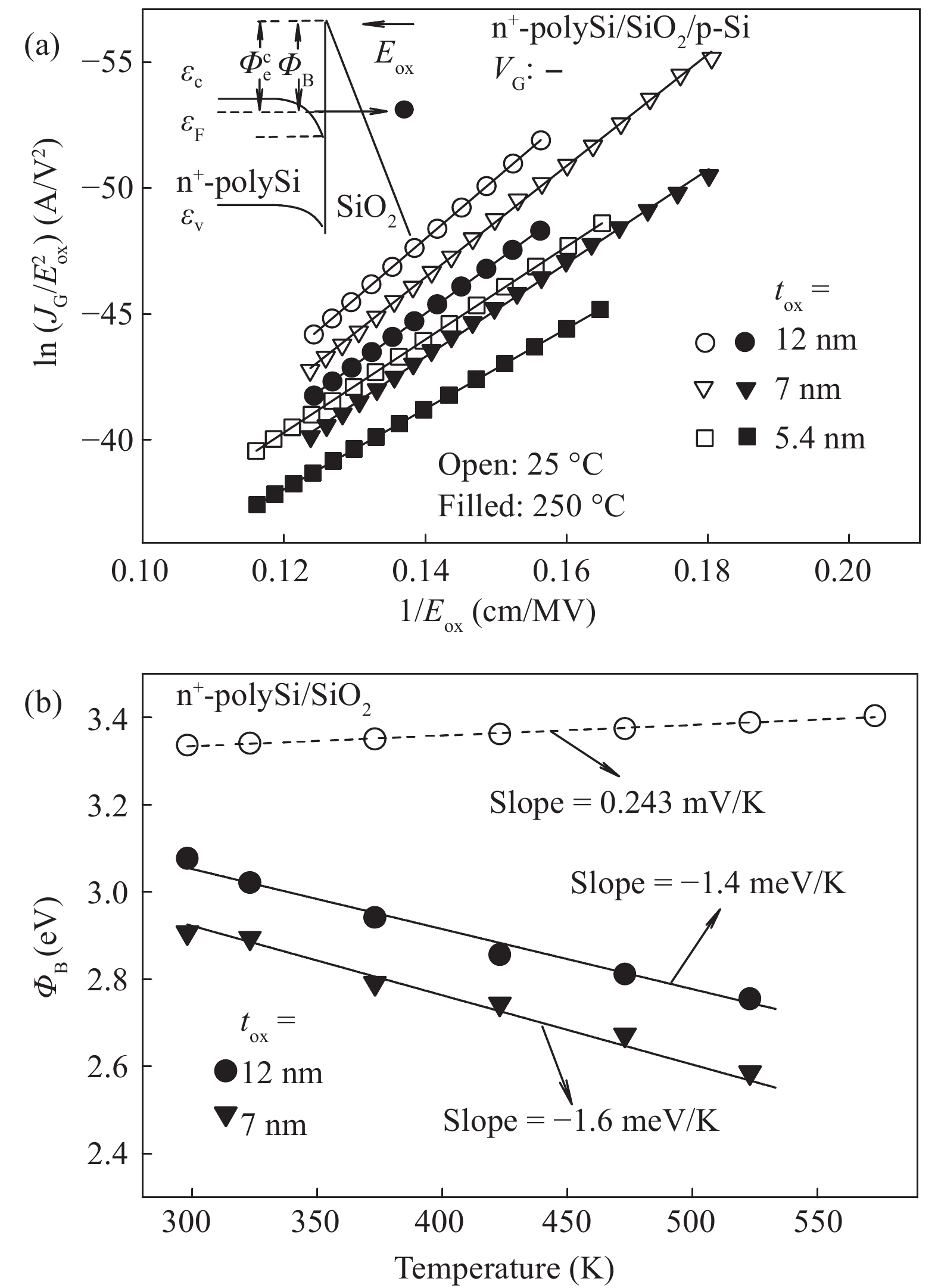
The conduction mechanism of gate leakage current through thermally grown silicon dioxide (SiO2) films on (100) p-type silicon has been investigated in detail under negative bias on the degenerately doped n-type polysilicon (n+-polySi) gate. The analysis utilizes the measured gate current density JG at high oxide fields Eox in 5.4 to 12 nm thick SiO2 films between 25 and 300 °C. The leakage current measured up to 300 °C was due to Fowler–Nordheim (FN) tunneling of electrons from the accumulated n +-polySi gate in conjunction with Poole Frenkel (PF) emission of trapped-electrons from the electron traps located at energy levels ranging from 0.6 to 1.12 eV (depending on the oxide thickness) below the SiO2 conduction band (CB). It was observed that PF emission current IPF dominates FN electron tunneling current IFN at oxide electric fields Eox between 6 and 10 MV/cm and throughout the temperature range studied here. Understanding of the mechanism of leakage current conduction through SiO2 films plays a crucial role in simulation of time-dependent dielectric breakdown (TDDB) of metaloxide–semiconductor (MOS) devices and to precisely predict the normal operating field or applied gate voltage for lifetime projection of the MOS integrated circuits.-
Keywords:
- FN tunneling,
- PF emission,
- image force lowering,
- trap depth
-
References
[1] Yang B L, Lai P T, Wong H. Conduction mechanisms in MOS gate dielectric films. Microelectron Reliab, 2004, 44: 709 doi: 10.1016/j.microrel.2004.01.013[2] Lenzlinger M, Snow E H. Fowler—Nordheim tunneling into thermally grown SiO2. J Appl Phys, 1969, 40: 278 doi: 10.1063/1.1657043[3] Weinberg Z A. Tunneling of electrons from Si into thermally grown SiO2. Solid-State Electron, 1977, 20: 11[4] Weinberg Z A. On tunneling in metal–oxide–silicon structures. J Appl Phys, 1982, 53: 5052 doi: 10.1063/1.331336[5] Krieger G, Swanson R M. Fowler—Nordheim electron tunneling in thin Si-SiO2-Al structures. J Appl Phys, 1981, 52: 5710 doi: 10.1063/1.329510[6] Depas M, Vermeire B, Mertens P W, et al. Determination of tunneling parameters in ultra-thin oxide layer poly-Si/SiO2/Si structures. Solid-State Electron, 1995, 38: 1465 doi: 10.1016/0038-1101(94)00269-L[7] Pananakakis G, Ghibaudo G, Kies R, et al. Temperature dependence of the Fowler—Nordheim current in metal—oxidedegenerate semiconductor structures. J Appl Phys, 1995, 78: 2635 doi: 10.1063/1.360124[8] Hadjadj A, Salace G, Petit C. Fowler-Nordheim conduction in polysilicon (n+)-oxide-silicon (p) structures: Limit of the classical treatment in the barrier height determination. J Appl Phys, 2001, 89: 7994 doi: 10.1063/1.1374479[9] Roca M, Laffont R, Micolau G, et al. A Modelisation of the temperature dependence of the Fowler—Nordheim current in EEPROM memories. Microelectron Reliab, 2009, 49: 1070 doi: 10.1016/j.microrel.2009.06.036[10] Aygun G, Roeder G, Erlbacher T, et al. Impact of temperature increments on tunneling barrier height and effective electron mass for plasma nitrided thin SiO2 layer on a large wafer area. J Appl Phys, 2010, 108: 073304 doi: 10.1063/1.3481348[11] Waters R, Zeghbroeck B V. On field emission from a semiconducting substrate. Appl Phys Lett, 1999, 75: 2410 doi: 10.1063/1.125030[12] Samanta P, Mandal K C. Leakage current conduction and reliability assessment of passivating thin silicon dioxide films on n-4H-SiC. Proceedings of SPIE (SPIE, Bellingham, WA, 2016), 2016, 9968: 99680E[13] Samanta P, Mandal K C. Leakage current conduction, hole injection, and time-dependent dielectric breakdown of n-4H-SiC MOS capacitors during positive bias temperature stress. J Appl Phys, 2017, 121: 034501 doi: 10.1063/1.4973674[14] Sze S M, Ng K K. Physics of semiconductor devices. New Jersey: John Wiley & Sons, Inc., 2007[15] Alay J L, Hirose M. The valence band alignment at ultrathin SiO2/Si interfaces. J Appl Phys, 1997, 81: 1606 doi: 10.1063/1.363895[16] Afanasev V V, Bassler M, Pensl G, et al. Band offsets and electronic structure of SiC/SiO2 interfaces. J Appl Phys, 1996, 79: 3108 doi: 10.1063/1.361254[17] Rossinelli M, Bosch M A. Reflectance spectrum of crystalline and vitreous SiO2 at low temperature. Phys Rev B, 1982, 25: 6482 doi: 10.1103/PhysRevB.25.6482[18] Persson C, Lindefelt U, Sernelius B E. Band gap narrowing in n-type and p-type 3C-, 2H-, 4H-, 6H-SiC, and Si. J Appl Phys, 1999, 86: 4419 doi: 10.1063/1.371380[19] Murphy E L, Good R H. Thermionic emission, field emission, and the transition region. Phys Rev, 1956, 102: 1464 doi: 10.1103/PhysRev.102.1464[20] Samanta P. Mechanistic analysis of temperature dependent current conduction through thin tunnel oxide in n+-polySi/SiO2/n+-Si structures. J Appl Phys, 2017, 122: 094502[21] Wolfram Research, Inc., Mathematica, Version 11.0, 2016 (Champaign, IL)[22] Banerjee S, Shen B, Chen I, et al. Conduction mechanisms in sputtered Ta2O5 on Si with an interfacial SiO2 layer. J Appl Phys, 1989, 65: 1140 doi: 10.1063/1.343052[23] Harrell W R, Gopalakrishnan C. Implications of advanced modeling on the observation of Poole–Frenkel effect saturation. Thin Solid Films, 2002, 405: 205 doi: 10.1016/S0040-6090(01)01752-7[24] Lu Z Y, Nicklaw J, Fleetwood D M, et al. Structure, properties, and dynamics of oxygen vacancies in amorphous SiO2. Phys Rev Lett, 2002, 89: 285505 doi: 10.1103/PhysRevLett.89.285505 -
Proportional views


 DownLoad:
