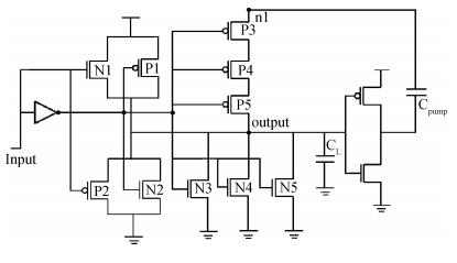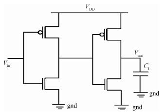
Fig. 1.
Conventional repeater
SEMICONDUCTOR INTEGRATED CIRCUITS
A. Karthikeyan and P.S. Mallick
Corresponding author: P. S. Mallick, Email: psmallick@vit.ac.in
Abstract: This paper proposes a repeater for boosting the speed of interconnects with low power dissipation. We have designed and implemented at 45 and 32 nm technology nodes. Delay and power dissipation performances are analyzed for various voltage levels at these technology nodes using Spice simulations. A significant reduction in delay and power dissipation are observed compared to a conventional repeater. The results show that the proposed high-speed low-power repeater has a reduced delay for higher load capacitance. The proposed repeater is also compared with LPTG CMOS repeater, and the results shows that the proposed repeater has reduced delay. The proposed repeater can be suitable for high-speed global interconnects and has the capacity to drive large loads.
Keywords: repeater, interconnects, delay, power dissipation, charge pump
| [1] |
Rabaey J, Chandrakasan A, Nikolic B. Digital integrated circuits:a design perspective. Prentice Hall of India, 2003
|
| [2] |
Sharma V K, Pattanaik M. VLSI scaling methods and low power CMOS buffer circuits. J Semicond, 2013, 34(9):095001 doi: 10.1088/1674-4926/34/9/095001
|
| [3] |
Banerjee K, Mehrotra A. A power-optimal repeater insertion methodology for global interconnects in nanometer designs. IEEE Trans Electron Devices, 2002, 49(11):2001 doi: 10.1109/TED.2002.804706
|
| [4] |
Alpert J C, Devgan A, Quay T S. Buffer insertion for noise and delay optimization. IEEE Trans Comput-Aided Des Integr Circuits Syst, 1999, 18(2):1633 http://citeseerx.ist.psu.edu/viewdoc/summary?doi=10.1.1.421.5332
|
| [5] |
Wang X, Liu W, Yu M. A distinctive O (mn) time algorithm for optimal buffer insertions. IEEE International Symposium on Quality Electronic Design, 2015, 16:293 https://www.mql5.com/en/market/mt4/indicator/paid/page8
|
| [6] |
Kaushik B K, Sarkar S, Agarwal R P, et al. Crosstalk analysis and repeater insertion in crosstalk aware coupled VLSI interconnects. Microelectron Int, 2006, 23(3):55 doi: 10.1108/13565360610680776
|
| [7] |
Kaushik B K, Agarwal R P, Sarkar S. Repeater insertion in crosstalk-aware inductively and capacitively coupled interconnects. Int J Circuit Theory Appl, 2011, 39(6):629 doi: 10.1002/cta.v39.6
|
| [8] |
Hasani F, Masoumi N. Interconnect sizing and spacing with consideration of buffer insertion for simultaneous crosstalk-delay optimization. International Conference on Design & Technology of Integrated Systems in Nanoscale Era, 2008, 3:1 http://citeseerx.ist.psu.edu/viewdoc/summary?doi=10.1.1.570.8616
|
| [9] |
Chandel R, Sarkar S, Agarwal R P. Repeater insertion in global interconnects in VLSI circuits. Microelectron Int, 2005, 22(1):43 doi: 10.1108/13565360510575549
|
| [10] |
Chandel R, Sarkar S, Agarwal R P. An analysis of interconnect delay minimization by low-voltage repeater insertion. Microelectron J, 2007, 38(4):649 doi: 10.1007/s10470-016-0860-8
|
| [11] |
Alizadeh A, Sarvari R. On temperature dependency of delay for local, intermediate, and repeater inserted global copper interconnects. IEEE Trans Very Large Scale Integr (VLSI) Syst, 2015, 23(12):3143 doi: 10.1109/TVLSI.2014.2379954
|
| [12] |
Libo Q, Zhangming Z, Ruixue D, et al. Circuit modeling and performance analysis of SWCNT bundle 3D interconnects. J Semicond, 2013, 34(9):095014 doi: 10.1088/1674-4926/34/9/095014
|
| [13] |
Zhao W S, Wang G, Sun L. Repeater insertion for carbon nanotube interconnects. IET Micro Nano Lett, 2014, 9(5):337 doi: 10.1049/mnl.2014.0001
|
| [14] |
Liang F, Wang G, Ding W. Estimation of time delay and repeater insertion in multiwall carbon nanotube interconnects. IEEE Trans Electron Devices, 2011, 58(8):2712 doi: 10.1109/TED.2011.2154334
|
| [15] |
Sathyakam P U, Mallick P S. Transient analysis of mixed carbon nanotube bundle interconnects. Electron Lett, 2011, 47(20):1134 doi: 10.1049/el.2011.1705
|
| [16] |
Sathyakam P U, Karthikeyan A, Mallick P S. Role of semiconducting carbon nanotubes in crosstalk reduction of CNT interconnects. IEEE Trans Nanotechnol, 2013, 12(5):662 doi: 10.1109/TNANO.2013.2272598
|
| [17] |
Sathyakam P U, Mallick P S. Towards realization of mixed carbon nanotube bundles as VLSI interconnects:a review. Nano Comm Netw, 2012, 3(3):175 doi: 10.1016/j.nancom.2012.09.004
|
| [18] |
Karthikeyan A, Mallick P S. Optimization techniques for CNT based VLSI interconnects-a review. J Circuits, Syst, Comput, 2017, 26(3):173002 doi: 10.1142/S0218126617300021?src=recsys
|
| [19] |
Saini S, Kumar A M, Veeramachaneni S. An alternative approach to buffer insertion for delay and power reduction in VLSI interconnects. IEEE International Conference on VLSI Design 2010, 23:411 doi: 10.1007/978-1-4614-1323-3
|
| [20] |
Mehri M, Kouhani M H M, Masoumi N, et al. New approach to VLSI buffer modeling considering overshooting effect. IEEE Trans Very Large Scale Integr (VLSI) Syst, 2013, 21(8):1568 doi: 10.1109/TVLSI.2012.2211629
|
| [21] |
Awwad F R, Nekili M, Ramachandran V, et al. On modeling of parallel repeater-insertion methodologies for SoC interconnects. IEEE Trans Circuits Syst, 2008, 55(1):322 doi: 10.1109/TCSI.2007.910538
|
| [22] |
Ho Y, Chen H K, Su C. Energy-effective sub-threshold interconnect design using high-boosting predrivers. IEEE J Emerg Sel Top Circuits Syst, 2012, 2(2):307 doi: 10.1109/JETCAS.2012.2193841
|
| [23] |
Shim K N, Hu J. Boostable repeater design for variation resilience in VLSI interconnects. IEEE Trans Very Large Scale Integr (VLSI) Syst, 2013, 21(9):1619 doi: 10.1109/TVLSI.2012.2212733
|
| [24] |
Kil J, Gu J, Kim C. A high-speed variation-tolerant interconnect technique for sub-threshold circuits using capacitive boosting. IEEE Trans Very Large Scale Integr (VLSI) Syst, 2008, 16(4):456 doi: 10.1109/TVLSI.2007.915455
|
| [25] |
Lee J, Ryu M, Kim Y. On-chip interconnect boosting technique by using of 10-nm double gate-all-around (DGAA) transistor. IEICE Electron Express, 2015, 12(12):1 http://scholarworks.unist.ac.kr/bitstream/201301/16423/1/000358128300003.pdf
|
| [26] |
Nalamalpu A, Srinivasan S, Burleson P W. Boosters for driving long on chip interconnects-design issues, interconnect synthesis, and comparison with repeaters. IEEE Trans Comput-Aided Des Integr Circuits Syst, 2002, 21(1):50 doi: 10.1109/43.974137
|
| [27] |
Nigussie E, Tuuna S, Plosila J. Boosting performance of selftimed delay-insensitive bit parallel on-chip interconnects. IET Circuits Dev Syst, 2011, 5(6):505 doi: 10.1049/iet-cds.2010.0300
|
| [28] |
Gholami M. Phase frequency detector using transmission gates for high speed applications. Int J Eng Trans A, 2016, 29(7):916 http://www.ije.ir/abstract/%7BVolume:29-Transactions:A-Number:7%7D/=2276
|
| [29] |
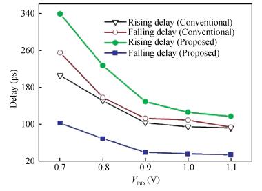
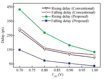
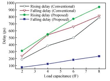
Table 1. Comparison with other published repeaters
 |
| [1] |
Rabaey J, Chandrakasan A, Nikolic B. Digital integrated circuits:a design perspective. Prentice Hall of India, 2003
|
| [2] |
Sharma V K, Pattanaik M. VLSI scaling methods and low power CMOS buffer circuits. J Semicond, 2013, 34(9):095001 doi: 10.1088/1674-4926/34/9/095001
|
| [3] |
Banerjee K, Mehrotra A. A power-optimal repeater insertion methodology for global interconnects in nanometer designs. IEEE Trans Electron Devices, 2002, 49(11):2001 doi: 10.1109/TED.2002.804706
|
| [4] |
Alpert J C, Devgan A, Quay T S. Buffer insertion for noise and delay optimization. IEEE Trans Comput-Aided Des Integr Circuits Syst, 1999, 18(2):1633 http://citeseerx.ist.psu.edu/viewdoc/summary?doi=10.1.1.421.5332
|
| [5] |
Wang X, Liu W, Yu M. A distinctive O (mn) time algorithm for optimal buffer insertions. IEEE International Symposium on Quality Electronic Design, 2015, 16:293 https://www.mql5.com/en/market/mt4/indicator/paid/page8
|
| [6] |
Kaushik B K, Sarkar S, Agarwal R P, et al. Crosstalk analysis and repeater insertion in crosstalk aware coupled VLSI interconnects. Microelectron Int, 2006, 23(3):55 doi: 10.1108/13565360610680776
|
| [7] |
Kaushik B K, Agarwal R P, Sarkar S. Repeater insertion in crosstalk-aware inductively and capacitively coupled interconnects. Int J Circuit Theory Appl, 2011, 39(6):629 doi: 10.1002/cta.v39.6
|
| [8] |
Hasani F, Masoumi N. Interconnect sizing and spacing with consideration of buffer insertion for simultaneous crosstalk-delay optimization. International Conference on Design & Technology of Integrated Systems in Nanoscale Era, 2008, 3:1 http://citeseerx.ist.psu.edu/viewdoc/summary?doi=10.1.1.570.8616
|
| [9] |
Chandel R, Sarkar S, Agarwal R P. Repeater insertion in global interconnects in VLSI circuits. Microelectron Int, 2005, 22(1):43 doi: 10.1108/13565360510575549
|
| [10] |
Chandel R, Sarkar S, Agarwal R P. An analysis of interconnect delay minimization by low-voltage repeater insertion. Microelectron J, 2007, 38(4):649 doi: 10.1007/s10470-016-0860-8
|
| [11] |
Alizadeh A, Sarvari R. On temperature dependency of delay for local, intermediate, and repeater inserted global copper interconnects. IEEE Trans Very Large Scale Integr (VLSI) Syst, 2015, 23(12):3143 doi: 10.1109/TVLSI.2014.2379954
|
| [12] |
Libo Q, Zhangming Z, Ruixue D, et al. Circuit modeling and performance analysis of SWCNT bundle 3D interconnects. J Semicond, 2013, 34(9):095014 doi: 10.1088/1674-4926/34/9/095014
|
| [13] |
Zhao W S, Wang G, Sun L. Repeater insertion for carbon nanotube interconnects. IET Micro Nano Lett, 2014, 9(5):337 doi: 10.1049/mnl.2014.0001
|
| [14] |
Liang F, Wang G, Ding W. Estimation of time delay and repeater insertion in multiwall carbon nanotube interconnects. IEEE Trans Electron Devices, 2011, 58(8):2712 doi: 10.1109/TED.2011.2154334
|
| [15] |
Sathyakam P U, Mallick P S. Transient analysis of mixed carbon nanotube bundle interconnects. Electron Lett, 2011, 47(20):1134 doi: 10.1049/el.2011.1705
|
| [16] |
Sathyakam P U, Karthikeyan A, Mallick P S. Role of semiconducting carbon nanotubes in crosstalk reduction of CNT interconnects. IEEE Trans Nanotechnol, 2013, 12(5):662 doi: 10.1109/TNANO.2013.2272598
|
| [17] |
Sathyakam P U, Mallick P S. Towards realization of mixed carbon nanotube bundles as VLSI interconnects:a review. Nano Comm Netw, 2012, 3(3):175 doi: 10.1016/j.nancom.2012.09.004
|
| [18] |
Karthikeyan A, Mallick P S. Optimization techniques for CNT based VLSI interconnects-a review. J Circuits, Syst, Comput, 2017, 26(3):173002 doi: 10.1142/S0218126617300021?src=recsys
|
| [19] |
Saini S, Kumar A M, Veeramachaneni S. An alternative approach to buffer insertion for delay and power reduction in VLSI interconnects. IEEE International Conference on VLSI Design 2010, 23:411 doi: 10.1007/978-1-4614-1323-3
|
| [20] |
Mehri M, Kouhani M H M, Masoumi N, et al. New approach to VLSI buffer modeling considering overshooting effect. IEEE Trans Very Large Scale Integr (VLSI) Syst, 2013, 21(8):1568 doi: 10.1109/TVLSI.2012.2211629
|
| [21] |
Awwad F R, Nekili M, Ramachandran V, et al. On modeling of parallel repeater-insertion methodologies for SoC interconnects. IEEE Trans Circuits Syst, 2008, 55(1):322 doi: 10.1109/TCSI.2007.910538
|
| [22] |
Ho Y, Chen H K, Su C. Energy-effective sub-threshold interconnect design using high-boosting predrivers. IEEE J Emerg Sel Top Circuits Syst, 2012, 2(2):307 doi: 10.1109/JETCAS.2012.2193841
|
| [23] |
Shim K N, Hu J. Boostable repeater design for variation resilience in VLSI interconnects. IEEE Trans Very Large Scale Integr (VLSI) Syst, 2013, 21(9):1619 doi: 10.1109/TVLSI.2012.2212733
|
| [24] |
Kil J, Gu J, Kim C. A high-speed variation-tolerant interconnect technique for sub-threshold circuits using capacitive boosting. IEEE Trans Very Large Scale Integr (VLSI) Syst, 2008, 16(4):456 doi: 10.1109/TVLSI.2007.915455
|
| [25] |
Lee J, Ryu M, Kim Y. On-chip interconnect boosting technique by using of 10-nm double gate-all-around (DGAA) transistor. IEICE Electron Express, 2015, 12(12):1 http://scholarworks.unist.ac.kr/bitstream/201301/16423/1/000358128300003.pdf
|
| [26] |
Nalamalpu A, Srinivasan S, Burleson P W. Boosters for driving long on chip interconnects-design issues, interconnect synthesis, and comparison with repeaters. IEEE Trans Comput-Aided Des Integr Circuits Syst, 2002, 21(1):50 doi: 10.1109/43.974137
|
| [27] |
Nigussie E, Tuuna S, Plosila J. Boosting performance of selftimed delay-insensitive bit parallel on-chip interconnects. IET Circuits Dev Syst, 2011, 5(6):505 doi: 10.1049/iet-cds.2010.0300
|
| [28] |
Gholami M. Phase frequency detector using transmission gates for high speed applications. Int J Eng Trans A, 2016, 29(7):916 http://www.ije.ir/abstract/%7BVolume:29-Transactions:A-Number:7%7D/=2276
|
| [29] |


Article views: 4945 Times PDF downloads: 82 Times Cited by: 0 Times
Received: 01 February 2017 Revised: 17 March 2017 Online: Published: 01 October 2017
| Citation: |
A. Karthikeyan, P.S. Mallick. High-speed and low-power repeater for VLSI interconnects[J]. Journal of Semiconductors, 2017, 38(10): 105006. doi: 10.1088/1674-4926/38/10/105006
****
A. Karthikeyan, P.S. Mallick. High-speed and low-power repeater for VLSI interconnects[J]. J. Semicond., 2017, 38(10): 105006. doi: 10.1088/1674-4926/38/10/105006.

|
| [1] |
Rabaey J, Chandrakasan A, Nikolic B. Digital integrated circuits:a design perspective. Prentice Hall of India, 2003
|
| [2] |
Sharma V K, Pattanaik M. VLSI scaling methods and low power CMOS buffer circuits. J Semicond, 2013, 34(9):095001 doi: 10.1088/1674-4926/34/9/095001
|
| [3] |
Banerjee K, Mehrotra A. A power-optimal repeater insertion methodology for global interconnects in nanometer designs. IEEE Trans Electron Devices, 2002, 49(11):2001 doi: 10.1109/TED.2002.804706
|
| [4] |
Alpert J C, Devgan A, Quay T S. Buffer insertion for noise and delay optimization. IEEE Trans Comput-Aided Des Integr Circuits Syst, 1999, 18(2):1633 http://citeseerx.ist.psu.edu/viewdoc/summary?doi=10.1.1.421.5332
|
| [5] |
Wang X, Liu W, Yu M. A distinctive O (mn) time algorithm for optimal buffer insertions. IEEE International Symposium on Quality Electronic Design, 2015, 16:293 https://www.mql5.com/en/market/mt4/indicator/paid/page8
|
| [6] |
Kaushik B K, Sarkar S, Agarwal R P, et al. Crosstalk analysis and repeater insertion in crosstalk aware coupled VLSI interconnects. Microelectron Int, 2006, 23(3):55 doi: 10.1108/13565360610680776
|
| [7] |
Kaushik B K, Agarwal R P, Sarkar S. Repeater insertion in crosstalk-aware inductively and capacitively coupled interconnects. Int J Circuit Theory Appl, 2011, 39(6):629 doi: 10.1002/cta.v39.6
|
| [8] |
Hasani F, Masoumi N. Interconnect sizing and spacing with consideration of buffer insertion for simultaneous crosstalk-delay optimization. International Conference on Design & Technology of Integrated Systems in Nanoscale Era, 2008, 3:1 http://citeseerx.ist.psu.edu/viewdoc/summary?doi=10.1.1.570.8616
|
| [9] |
Chandel R, Sarkar S, Agarwal R P. Repeater insertion in global interconnects in VLSI circuits. Microelectron Int, 2005, 22(1):43 doi: 10.1108/13565360510575549
|
| [10] |
Chandel R, Sarkar S, Agarwal R P. An analysis of interconnect delay minimization by low-voltage repeater insertion. Microelectron J, 2007, 38(4):649 doi: 10.1007/s10470-016-0860-8
|
| [11] |
Alizadeh A, Sarvari R. On temperature dependency of delay for local, intermediate, and repeater inserted global copper interconnects. IEEE Trans Very Large Scale Integr (VLSI) Syst, 2015, 23(12):3143 doi: 10.1109/TVLSI.2014.2379954
|
| [12] |
Libo Q, Zhangming Z, Ruixue D, et al. Circuit modeling and performance analysis of SWCNT bundle 3D interconnects. J Semicond, 2013, 34(9):095014 doi: 10.1088/1674-4926/34/9/095014
|
| [13] |
Zhao W S, Wang G, Sun L. Repeater insertion for carbon nanotube interconnects. IET Micro Nano Lett, 2014, 9(5):337 doi: 10.1049/mnl.2014.0001
|
| [14] |
Liang F, Wang G, Ding W. Estimation of time delay and repeater insertion in multiwall carbon nanotube interconnects. IEEE Trans Electron Devices, 2011, 58(8):2712 doi: 10.1109/TED.2011.2154334
|
| [15] |
Sathyakam P U, Mallick P S. Transient analysis of mixed carbon nanotube bundle interconnects. Electron Lett, 2011, 47(20):1134 doi: 10.1049/el.2011.1705
|
| [16] |
Sathyakam P U, Karthikeyan A, Mallick P S. Role of semiconducting carbon nanotubes in crosstalk reduction of CNT interconnects. IEEE Trans Nanotechnol, 2013, 12(5):662 doi: 10.1109/TNANO.2013.2272598
|
| [17] |
Sathyakam P U, Mallick P S. Towards realization of mixed carbon nanotube bundles as VLSI interconnects:a review. Nano Comm Netw, 2012, 3(3):175 doi: 10.1016/j.nancom.2012.09.004
|
| [18] |
Karthikeyan A, Mallick P S. Optimization techniques for CNT based VLSI interconnects-a review. J Circuits, Syst, Comput, 2017, 26(3):173002 doi: 10.1142/S0218126617300021?src=recsys
|
| [19] |
Saini S, Kumar A M, Veeramachaneni S. An alternative approach to buffer insertion for delay and power reduction in VLSI interconnects. IEEE International Conference on VLSI Design 2010, 23:411 doi: 10.1007/978-1-4614-1323-3
|
| [20] |
Mehri M, Kouhani M H M, Masoumi N, et al. New approach to VLSI buffer modeling considering overshooting effect. IEEE Trans Very Large Scale Integr (VLSI) Syst, 2013, 21(8):1568 doi: 10.1109/TVLSI.2012.2211629
|
| [21] |
Awwad F R, Nekili M, Ramachandran V, et al. On modeling of parallel repeater-insertion methodologies for SoC interconnects. IEEE Trans Circuits Syst, 2008, 55(1):322 doi: 10.1109/TCSI.2007.910538
|
| [22] |
Ho Y, Chen H K, Su C. Energy-effective sub-threshold interconnect design using high-boosting predrivers. IEEE J Emerg Sel Top Circuits Syst, 2012, 2(2):307 doi: 10.1109/JETCAS.2012.2193841
|
| [23] |
Shim K N, Hu J. Boostable repeater design for variation resilience in VLSI interconnects. IEEE Trans Very Large Scale Integr (VLSI) Syst, 2013, 21(9):1619 doi: 10.1109/TVLSI.2012.2212733
|
| [24] |
Kil J, Gu J, Kim C. A high-speed variation-tolerant interconnect technique for sub-threshold circuits using capacitive boosting. IEEE Trans Very Large Scale Integr (VLSI) Syst, 2008, 16(4):456 doi: 10.1109/TVLSI.2007.915455
|
| [25] |
Lee J, Ryu M, Kim Y. On-chip interconnect boosting technique by using of 10-nm double gate-all-around (DGAA) transistor. IEICE Electron Express, 2015, 12(12):1 http://scholarworks.unist.ac.kr/bitstream/201301/16423/1/000358128300003.pdf
|
| [26] |
Nalamalpu A, Srinivasan S, Burleson P W. Boosters for driving long on chip interconnects-design issues, interconnect synthesis, and comparison with repeaters. IEEE Trans Comput-Aided Des Integr Circuits Syst, 2002, 21(1):50 doi: 10.1109/43.974137
|
| [27] |
Nigussie E, Tuuna S, Plosila J. Boosting performance of selftimed delay-insensitive bit parallel on-chip interconnects. IET Circuits Dev Syst, 2011, 5(6):505 doi: 10.1049/iet-cds.2010.0300
|
| [28] |
Gholami M. Phase frequency detector using transmission gates for high speed applications. Int J Eng Trans A, 2016, 29(7):916 http://www.ije.ir/abstract/%7BVolume:29-Transactions:A-Number:7%7D/=2276
|
| [29] |

 WeChat ID
Journal of Semiconductors © 2017 All Rights Reserved 京ICP备05085259号-2

 DownLoad: