


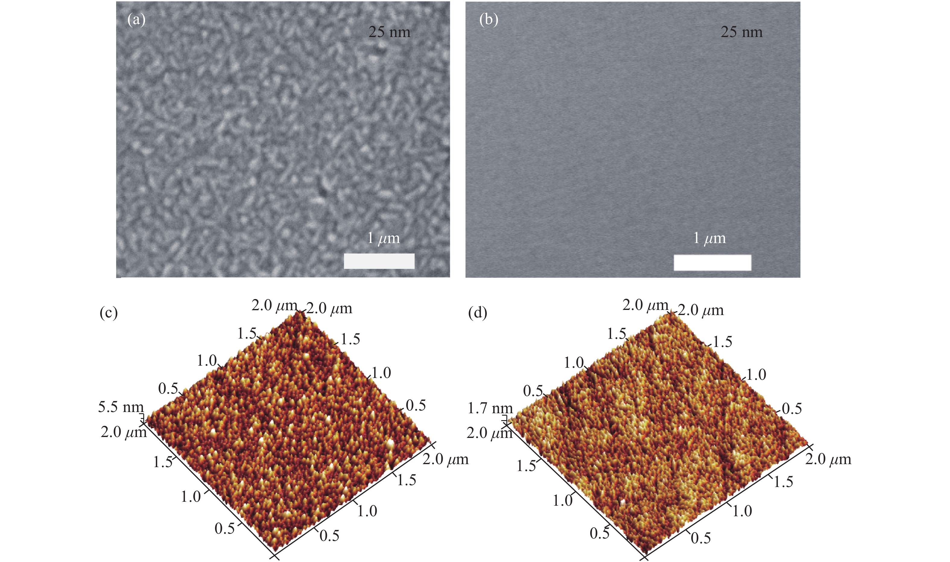
Fig. 1.
(Color online) The SEM and AFM images of nucleation layers grown on sapphire. (a, c) The 25-nm-thick in-situ NL. (b, d) The 25-nm-thick SNL.
SEMICONDUCTOR MATERIALS
Zejie Du1, 2, Ruifei Duan1, , Tongbo Wei1, Shuo Zhang1, Junxi Wang1, Xiaoyan Yi1, Yiping Zeng1, Junxue Ran1, Jinmin Li1 and Boyu Dong3
Corresponding author: Ruifei Duan, duanrf@semi.ac.cn
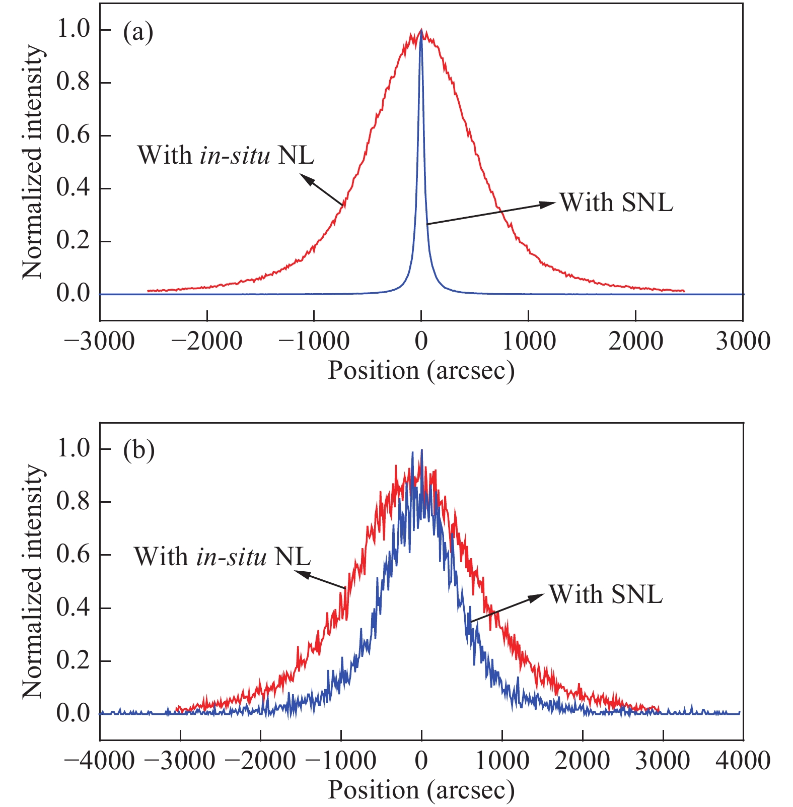
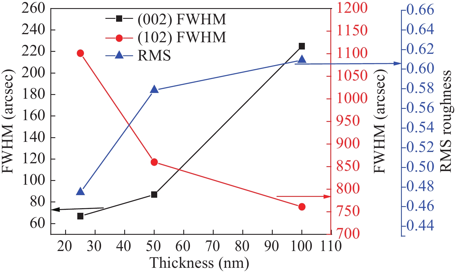
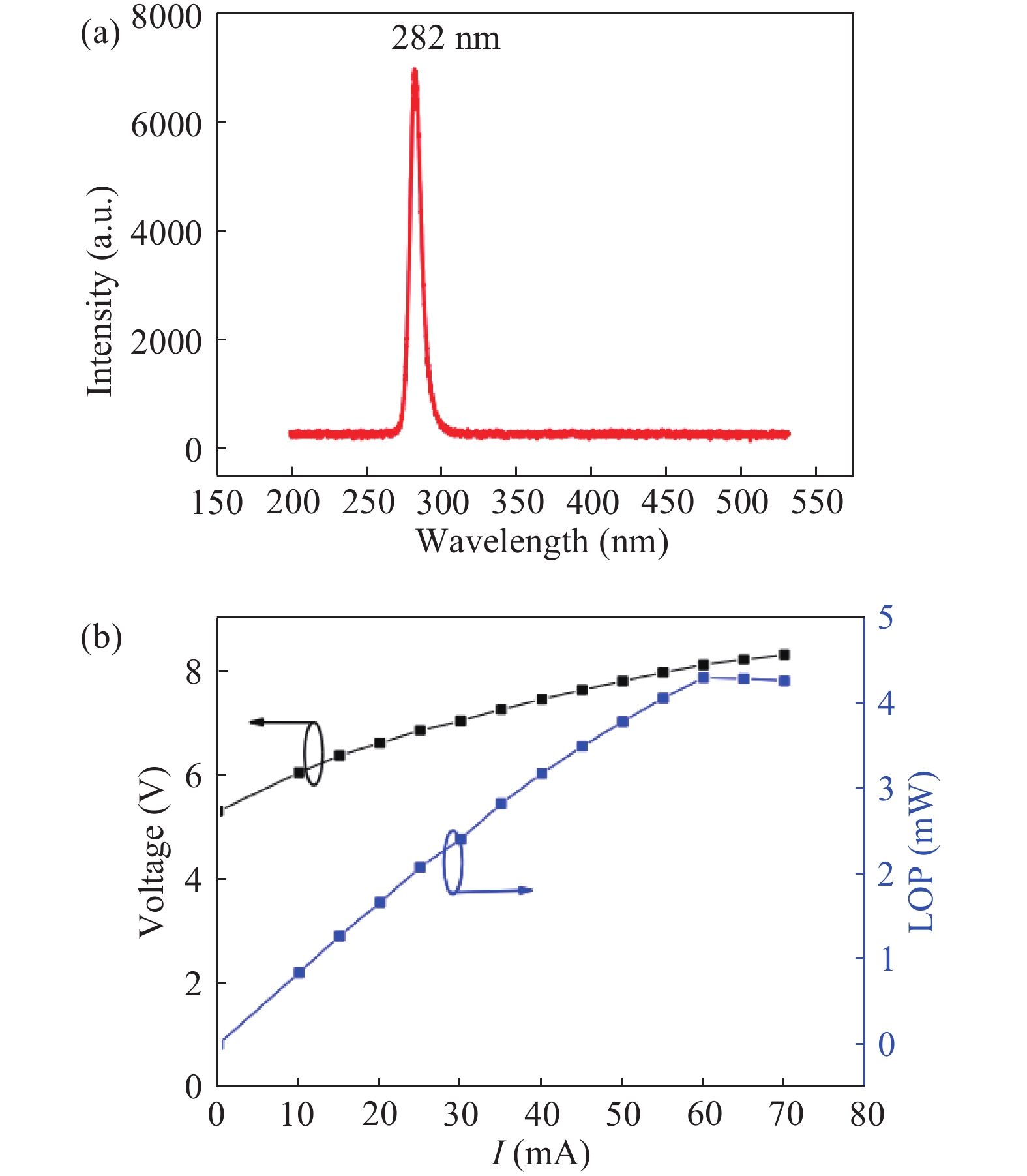
Abstract: High-quality AlN layers with low-density threading dislocations are indispensable for high-efficiency deep ultraviolet light-emitting diodes (UV-LEDs). In this work, a high-temperature AlN epitaxial layer was grown on sputtered AlN layer (used as nucleation layer, SNL) by a high-yield industrial metalorganic vapor phase epitaxy (MOVPE). The full width half maximum (FWHM) of the rocking curve shows that the AlN epitaxial layer with SNL has good crystal quality. Furthermore, the relationships between the thickness of SNL and the FWHM values of (002) and (102) peaks were also studied. Finally, utilizing an SNL to enhance the quality of the epitaxial layer, deep UV-LEDs at 282 nm were successfully realized on sapphire substrate by the high-yield industrial MOVPE. The light-output power (LOP) of a deep UV-LED reaches 1.65 mW at 20 mA with external quantum efficiency of 1.87%. In addition, the saturation LOP of the deep UV-LED is 4.31 mW at an injection current of 60 mA. Hence, our studies supply a possible process to grow commercial deep UV-LEDs in high throughput industrial MOVPE, which can increase yield, at lower cost.
Keywords: metalorganic vapor phase epitaxy, aluminum nitride, deep UV-LED
| [1] |
Shur M, Gaska R. Deep-ultraviolet light-emitting diodes. IEEE Trans Electron Devices, 2010, 57: 12 doi: 10.1109/TED.2009.2033768
|
| [2] |
Hideki H, Noritoshi M, Sachie F, et al. Recent progress and future prospects of AlGaN-based high-efficiency deep-ultraviolet light-emitting diodes. Jpn J Appl Phys, 2014, 53: 100209 doi: 10.7567/JJAP.53.100209
|
| [3] |
Dalmau R, Moody B, Schlesser R, et al. Growth and characterization of AlN and AlGaN epitaxial films on AlN single crystal substrates. J Electrochem Soc, 2011, 158: H530 doi: 10.1149/1.3560527
|
| [4] |
Ambacher O. Growth and applications of Group III-nitrides. J Phys D, 1998, 31: 2653 doi: 10.1088/0022-3727/31/20/001
|
| [5] |
Kakanakovageorgieva A, Nilsson D, Janzen E G. High-quality AlN layers grown by hot-wall MOCVD at reduced temperatures. J Cryst Growth, 2012, 338: 52 doi: 10.1016/j.jcrysgro.2011.10.052
|
| [6] |
Lobanova A V, Mazaev K, Talalaev R A, et al. Effect of V/III ratio in AlN and AlGaN MOVPE. J Cryst Growth, 2006, 287: 601 doi: 10.1016/j.jcrysgro.2005.10.083
|
| [7] |
Nakamura F, Hashimoto S, Hara M, et al. AlN and AlGaN growth using low-pressure metalorganic chemical vapor deposition. J Cryst Growth, 1998, 195: 280 doi: 10.1016/S0022-0248(98)00668-X
|
| [8] |
Reentilä O, Brunner F, Knauer A, et al. Effect of the AlN nucleation layer growth on AlN material quality. J Cryst Growth, 2008, 310: 4932 doi: 10.1016/j.jcrysgro.2008.07.083
|
| [9] |
Hirayama H, Yatabe T, Noguchi N, et al. 231–261 nm AlGaN deep-ultraviolet light-emitting diodes fabricated on AlN multilayer buffers grown by ammonia pulse-flow method on sapphire. Appl Phys Lett, 2007, 91: 071901 doi: 10.1063/1.2770662
|
| [10] |
Zeimer U, Kueller V, Knauer A, et al. High quality AlGaN grown on ELO AlN/sapphire templates. J Cryst Growth, 2013, 377: 32 doi: 10.1016/j.jcrysgro.2013.04.041
|
| [11] |
He L, Yang D, Ni G. AlGaN epitaxial technology, technology for advanced focal plane arrays of HgCdTe and AlGaN. Berlin, Heidelberg: Springer, 2016: 265
|
| [12] |
Chen C H, Liu H, Steigerwald D, et al. A study of parasitic reactions between NH3 and TMGa or TMAI. J Electron Mater, 1996, 25: 1004 doi: 10.1007/BF02666736
|
| [13] |
Creighton J R, Wang G T, Breiland W G, et al. Nature of the parasitic chemistry during AlGaInN OMVPE. J Cryst Growth, 2004, 261: 204 doi: 10.1016/j.jcrysgro.2003.11.074
|
| [14] |
Nakamura K, Makino O, Tachibana A, et al. Quantum chemical study of parasitic reaction in III–V nitride semiconductor crystal growth. J Organometal Chem, 2000, 611: 514 doi: 10.1016/S0022-328X(00)00403-4
|
| [15] |
Lee C Y, Tzou A J, Lin B C, et al. Efficiency improvement of GaN-based ultraviolet light-emitting diodes with reactive plasma deposited AlN nucleation layer on patterned sapphire substrate. Nanoscale Res Lett, 2014, 9: 505 doi: 10.1186/1556-276X-9-505
|
| [16] |
Wang X, Su X, Hu F, et al. Growth AlxGa1−xN films on Si substrates by magnetron sputtering and high ammoniated two-step method. J Alloys Compd, 2016, 667: 346 doi: 10.1016/j.jallcom.2016.01.191
|
| [17] |
Lai W, Yen C, Yang Y, et al. GaN-based ultraviolet light emitting diodes with ex situ sputtered AlN nucleation layer. J Display Technol, 2013, 9: 895 doi: 10.1109/JDT.2013.2264455
|
| [18] |
Chiu C, Lin Y, Tsai M, et al. Improved output power of GaN-based ultraviolet light-emitting diodes with sputtered AlN nucleation layer. J Cryst Growth, 2015, 414: 258 doi: 10.1016/j.jcrysgro.2014.10.013
|
| [19] |
Dong P, Yan J, Wang J, et al. 282-nm AlGaN-based deep ultraviolet light-emitting diodes with improved performance on nano-patterned sapphire substrates. Appl Phys Lett, 2013, 102: 241113 doi: 10.1063/1.4812237
|
| [20] |
Pantha B N, Dahal R, Nakarmi M L, et al. Correlation between optoelectronic and structural properties and epilayer thickness of AlN. Appl Phys Lett, 2007, 90: 241101 doi: 10.1063/1.2747662
|
| [21] |
Moram M A, Vickers M E. X-ray diffraction of III-nitrides. Rep Prog Phys, 2009, 72: 36502 doi: 10.1088/0034-4885/72/3/036502
|
| [22] |
Thapa S B, Hertkorn J, Scholz F, et al. Growth and studies of Si-doped AlN layers. J Cryst Growth, 2008, 310: 4939 doi: 10.1016/j.jcrysgro.2008.07.091
|
| [23] |
Zhao D G, Jiang D S, Zhu J J, et al. The influence of V/III ratio in the initial growth stage on the properties of GaN epilayer deposited on low temperature AlN buffer layer. J Cryst Growth, 2007, 303: 414 doi: 10.1016/j.jcrysgro.2007.01.019
|
| [24] |
Zhang L, Xu F, Wang M, et al. High-quality AlN epitaxy on sapphire substrates with sputtered buffer layers. Superlattices Microstruct, 2017, 105: 34 doi: 10.1016/j.spmi.2017.03.013
|
| [25] |
Bai J, Wang T, Parbrook P J, et al. A study of dislocations in AlN and GaN films grown on sapphire substrates. J Cryst Growth, 2005, 282: 290 doi: 10.1016/j.jcrysgro.2005.05.023
|
| [26] |
Kneissl M, Kolbe T, Chua C, et al. Advances in group III-nitride-based deep UV light-emitting diode technology. Semicond Sci Technol, 2011, 26: 014036 doi: 10.1088/0268-1242/26/1/014036
|


Article views: 4722 Times PDF downloads: 71 Times Cited by: 0 Times
Received: 10 April 2017 Revised: 16 May 2017 Online: Uncorrected proof: 30 October 2017Accepted Manuscript: 13 November 2017Published: 01 November 2017
| Citation: |
Zejie Du, Ruifei Duan, Tongbo Wei, Shuo Zhang, Junxi Wang, Xiaoyan Yi, Yiping Zeng, Junxue Ran, Jinmin Li, Boyu Dong. Producing deep UV-LEDs in high-yield MOVPE by improving AlN crystal quality with sputtered AlN nucleation layer[J]. Journal of Semiconductors, 2017, 38(11): 113003. doi: 10.1088/1674-4926/38/11/113003
****
Z J Du, R F Duan, T B Wei, S Zhang, J X Wang, X Y Yi, Y P Zeng, J X Ran, J M Li, B Y Dong. Producing deep UV-LEDs in high-yield MOVPE by improving AlN crystal quality with sputtered AlN nucleation layer[J]. J. Semicond., 2017, 38(11): 113003. doi: 10.1088/1674-4926/38/11/113003.

|
| [1] |
Shur M, Gaska R. Deep-ultraviolet light-emitting diodes. IEEE Trans Electron Devices, 2010, 57: 12 doi: 10.1109/TED.2009.2033768
|
| [2] |
Hideki H, Noritoshi M, Sachie F, et al. Recent progress and future prospects of AlGaN-based high-efficiency deep-ultraviolet light-emitting diodes. Jpn J Appl Phys, 2014, 53: 100209 doi: 10.7567/JJAP.53.100209
|
| [3] |
Dalmau R, Moody B, Schlesser R, et al. Growth and characterization of AlN and AlGaN epitaxial films on AlN single crystal substrates. J Electrochem Soc, 2011, 158: H530 doi: 10.1149/1.3560527
|
| [4] |
Ambacher O. Growth and applications of Group III-nitrides. J Phys D, 1998, 31: 2653 doi: 10.1088/0022-3727/31/20/001
|
| [5] |
Kakanakovageorgieva A, Nilsson D, Janzen E G. High-quality AlN layers grown by hot-wall MOCVD at reduced temperatures. J Cryst Growth, 2012, 338: 52 doi: 10.1016/j.jcrysgro.2011.10.052
|
| [6] |
Lobanova A V, Mazaev K, Talalaev R A, et al. Effect of V/III ratio in AlN and AlGaN MOVPE. J Cryst Growth, 2006, 287: 601 doi: 10.1016/j.jcrysgro.2005.10.083
|
| [7] |
Nakamura F, Hashimoto S, Hara M, et al. AlN and AlGaN growth using low-pressure metalorganic chemical vapor deposition. J Cryst Growth, 1998, 195: 280 doi: 10.1016/S0022-0248(98)00668-X
|
| [8] |
Reentilä O, Brunner F, Knauer A, et al. Effect of the AlN nucleation layer growth on AlN material quality. J Cryst Growth, 2008, 310: 4932 doi: 10.1016/j.jcrysgro.2008.07.083
|
| [9] |
Hirayama H, Yatabe T, Noguchi N, et al. 231–261 nm AlGaN deep-ultraviolet light-emitting diodes fabricated on AlN multilayer buffers grown by ammonia pulse-flow method on sapphire. Appl Phys Lett, 2007, 91: 071901 doi: 10.1063/1.2770662
|
| [10] |
Zeimer U, Kueller V, Knauer A, et al. High quality AlGaN grown on ELO AlN/sapphire templates. J Cryst Growth, 2013, 377: 32 doi: 10.1016/j.jcrysgro.2013.04.041
|
| [11] |
He L, Yang D, Ni G. AlGaN epitaxial technology, technology for advanced focal plane arrays of HgCdTe and AlGaN. Berlin, Heidelberg: Springer, 2016: 265
|
| [12] |
Chen C H, Liu H, Steigerwald D, et al. A study of parasitic reactions between NH3 and TMGa or TMAI. J Electron Mater, 1996, 25: 1004 doi: 10.1007/BF02666736
|
| [13] |
Creighton J R, Wang G T, Breiland W G, et al. Nature of the parasitic chemistry during AlGaInN OMVPE. J Cryst Growth, 2004, 261: 204 doi: 10.1016/j.jcrysgro.2003.11.074
|
| [14] |
Nakamura K, Makino O, Tachibana A, et al. Quantum chemical study of parasitic reaction in III–V nitride semiconductor crystal growth. J Organometal Chem, 2000, 611: 514 doi: 10.1016/S0022-328X(00)00403-4
|
| [15] |
Lee C Y, Tzou A J, Lin B C, et al. Efficiency improvement of GaN-based ultraviolet light-emitting diodes with reactive plasma deposited AlN nucleation layer on patterned sapphire substrate. Nanoscale Res Lett, 2014, 9: 505 doi: 10.1186/1556-276X-9-505
|
| [16] |
Wang X, Su X, Hu F, et al. Growth AlxGa1−xN films on Si substrates by magnetron sputtering and high ammoniated two-step method. J Alloys Compd, 2016, 667: 346 doi: 10.1016/j.jallcom.2016.01.191
|
| [17] |
Lai W, Yen C, Yang Y, et al. GaN-based ultraviolet light emitting diodes with ex situ sputtered AlN nucleation layer. J Display Technol, 2013, 9: 895 doi: 10.1109/JDT.2013.2264455
|
| [18] |
Chiu C, Lin Y, Tsai M, et al. Improved output power of GaN-based ultraviolet light-emitting diodes with sputtered AlN nucleation layer. J Cryst Growth, 2015, 414: 258 doi: 10.1016/j.jcrysgro.2014.10.013
|
| [19] |
Dong P, Yan J, Wang J, et al. 282-nm AlGaN-based deep ultraviolet light-emitting diodes with improved performance on nano-patterned sapphire substrates. Appl Phys Lett, 2013, 102: 241113 doi: 10.1063/1.4812237
|
| [20] |
Pantha B N, Dahal R, Nakarmi M L, et al. Correlation between optoelectronic and structural properties and epilayer thickness of AlN. Appl Phys Lett, 2007, 90: 241101 doi: 10.1063/1.2747662
|
| [21] |
Moram M A, Vickers M E. X-ray diffraction of III-nitrides. Rep Prog Phys, 2009, 72: 36502 doi: 10.1088/0034-4885/72/3/036502
|
| [22] |
Thapa S B, Hertkorn J, Scholz F, et al. Growth and studies of Si-doped AlN layers. J Cryst Growth, 2008, 310: 4939 doi: 10.1016/j.jcrysgro.2008.07.091
|
| [23] |
Zhao D G, Jiang D S, Zhu J J, et al. The influence of V/III ratio in the initial growth stage on the properties of GaN epilayer deposited on low temperature AlN buffer layer. J Cryst Growth, 2007, 303: 414 doi: 10.1016/j.jcrysgro.2007.01.019
|
| [24] |
Zhang L, Xu F, Wang M, et al. High-quality AlN epitaxy on sapphire substrates with sputtered buffer layers. Superlattices Microstruct, 2017, 105: 34 doi: 10.1016/j.spmi.2017.03.013
|
| [25] |
Bai J, Wang T, Parbrook P J, et al. A study of dislocations in AlN and GaN films grown on sapphire substrates. J Cryst Growth, 2005, 282: 290 doi: 10.1016/j.jcrysgro.2005.05.023
|
| [26] |
Kneissl M, Kolbe T, Chua C, et al. Advances in group III-nitride-based deep UV light-emitting diode technology. Semicond Sci Technol, 2011, 26: 014036 doi: 10.1088/0268-1242/26/1/014036
|

 WeChat ID
Journal of Semiconductors © 2017 All Rights Reserved 京ICP备05085259号-2

 DownLoad:

