


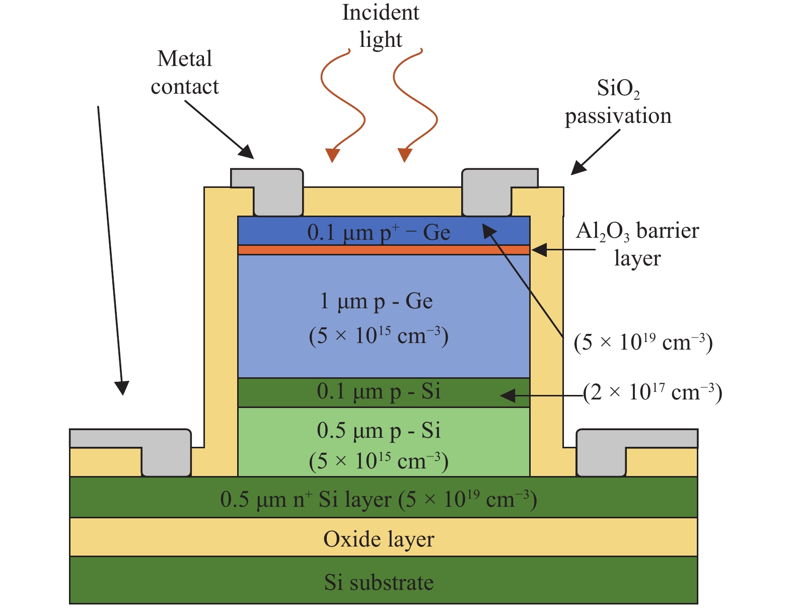
Fig. 1.
(Color online) Schematic of the Ge/Si tunneling avalanche photodiode (TAPD).
SEMICONDUCTOR DEVICES
Wenzhou Wu1, 2, Buwen Cheng1, 2, , Jun Zheng1, 2, Zhi Liu1, 2, Chuanbo Li1, 2, Yuhua Zuo1, 2 and Chunlai Xue1, 2
Corresponding author: Buwen Cheng. Email: cbw@semi.ac.cn
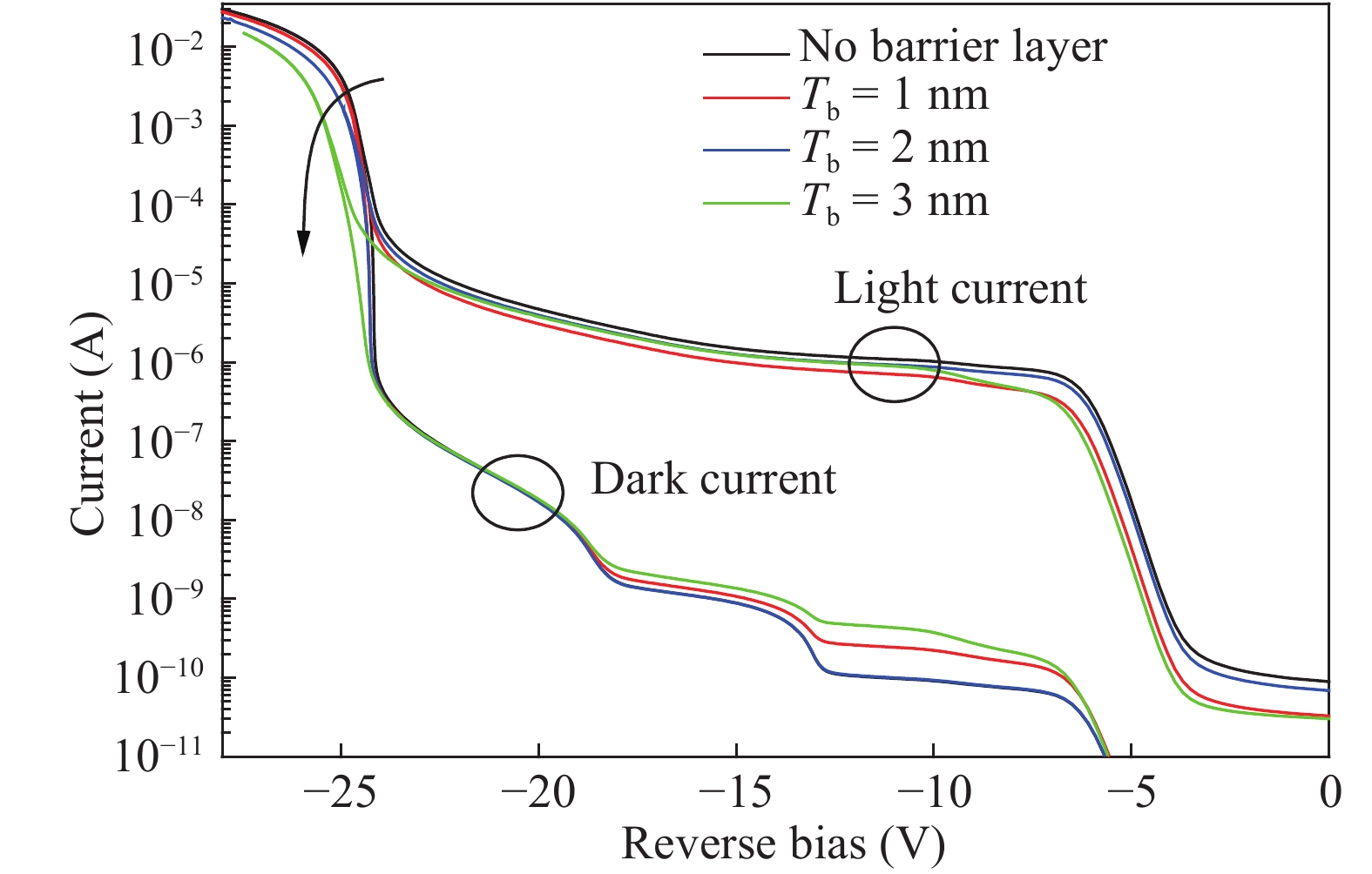
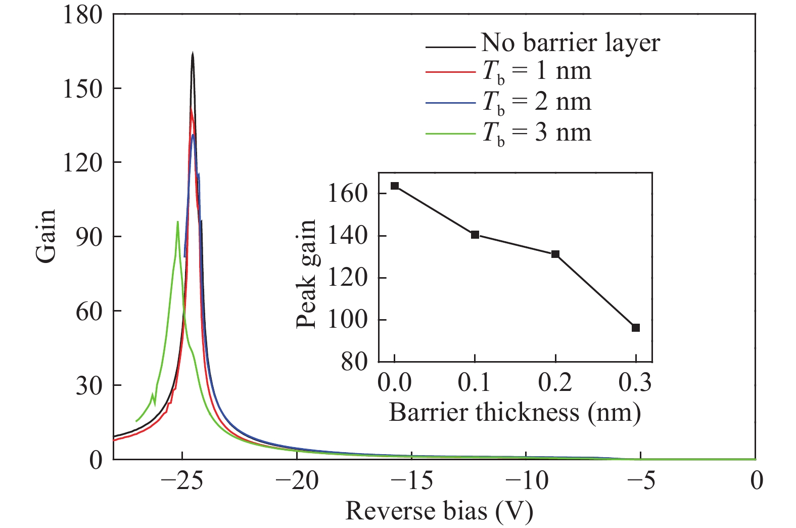
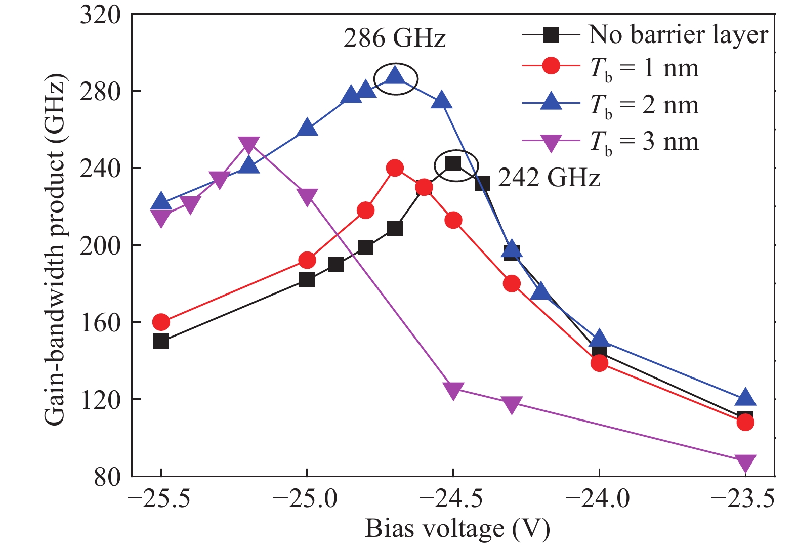
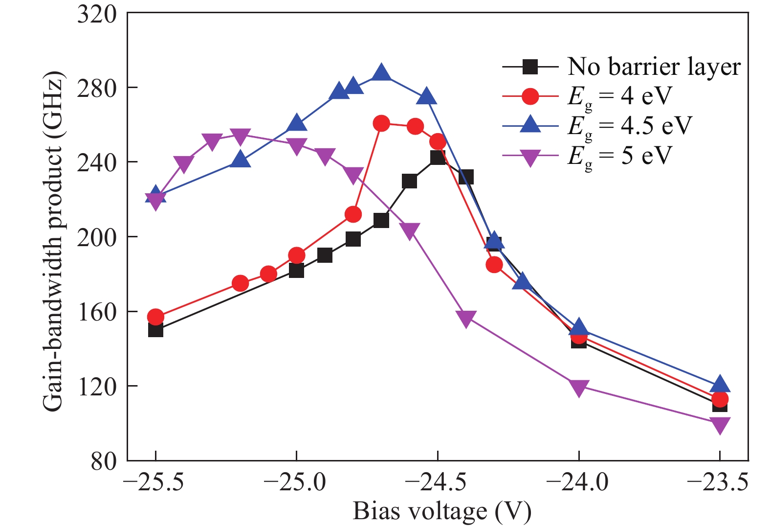
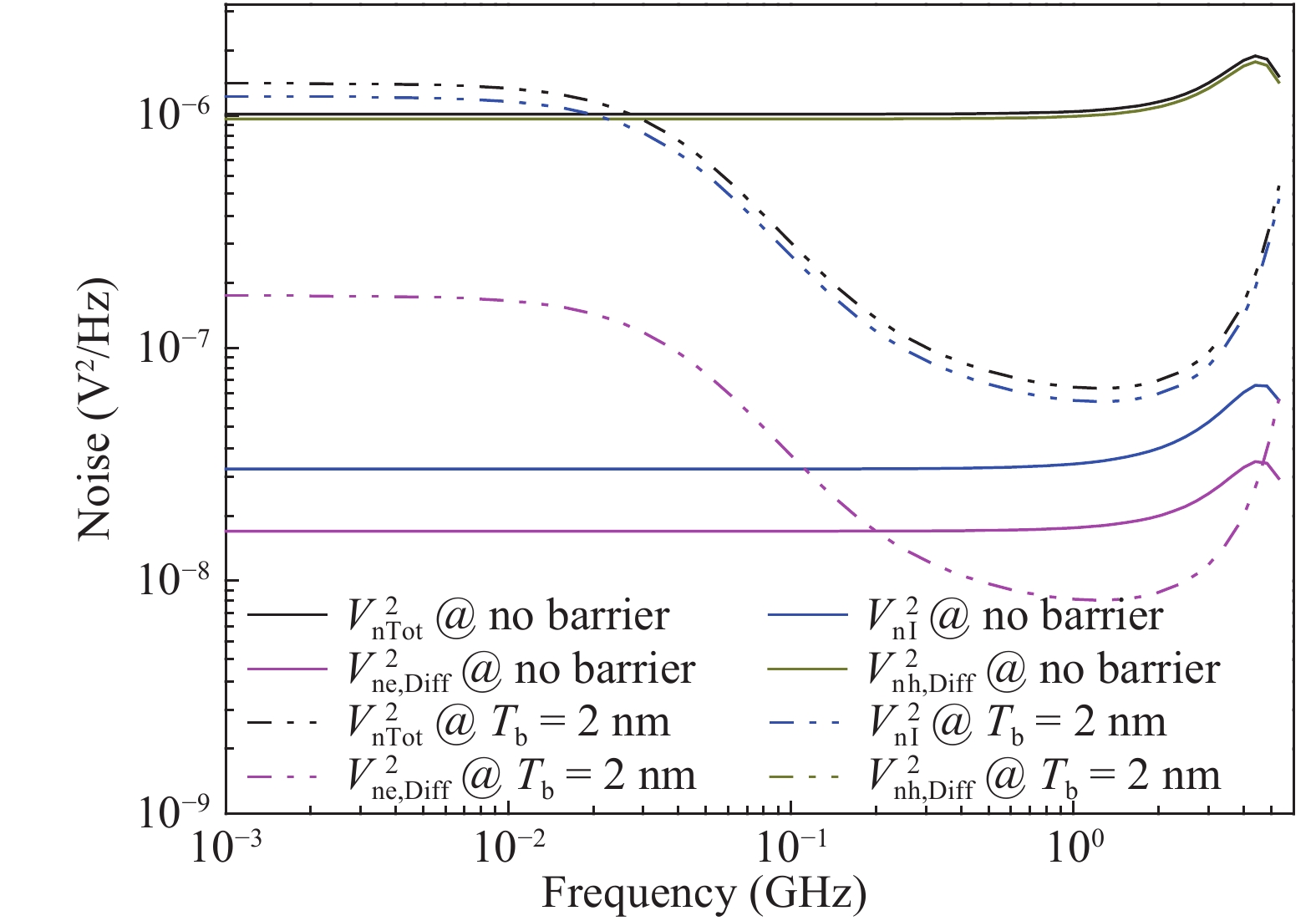
Abstract: This study presents a theoretical investigation of a novel Ge/Si tunneling avalanche photodiode (TAPD) with an ultra-thin barrier layer between the absorption and p+ contact layer. A high-frequency tunneling effect is introduced into the structure of the barrier layer to increase the high-frequency response when frequency is larger than 0.1 GHz, and the −3 dB bandwidth of the device increases evidently. The results demonstrate that the avalanche gain and −3 dB bandwidth of the TAPD can be influenced by the thickness and bandgap of the barrier layer. When the barrier thickness is 2 nm and the bandgap is 4.5 eV, the avalanche gain loss is negligible and the gain-bandwidth product of the TAPD is 286 GHz, which is 18% higher than that of an avalanche photodiode without a barrier layer. The total noise in the TAPD was an order of magnitude smaller than that in APD without barrier layer.
Keywords: avalanche photodiode, high-frequency tunneling effect, high gain-bandwidth product, fiber optic communication
| [1] |
Xu J, Chen X S, Wang W J, et al. Extracting dark current components and characteristics parameters for InGaAs/InP avalanche photodiodes. Infrared Phys Technol, 2016, 76: 468 doi: 10.1016/j.infrared.2016.04.004
|
| [2] |
Dong Y, Wang W, Lee S Y. Avalanche photodiode featuring germanium–tin multiple quantum wells on silicon: extending photodetection to wavelengths of 2 μm and beyond. 2015 IEEE International Electron Devices Meeting (IEDM), 2015: 787
|
| [3] |
Zhu S Y, Ang K W, Rustagi S C, et al. Waveguided Ge/Si avalanche photodiode with separate vertical SEG-Ge absorption, lateral Si charge, and multiplication configuration. IEEE Electron Device Lett, 2009, 30(9): 934 doi: 10.1109/LED.2009.2025782
|
| [4] |
Huang Z H, Liang D, Santori C, et al. Low-voltage Si–Ge avalanche photodiode. 2015 IEEE 12th International Conference on Group IV Photonics (GFP), 2015: 41
|
| [5] |
Liu H D, Pan H P, Hu C, et al. Avalanche photodiode punch-through gain determination through excess. J Appl Phys, 2009, 106: 064507 doi: 10.1063/1.3226659
|
| [6] |
Kang Y M, Liu H D, Morse M, et al. Monolithic germanium/silicon avalanche photodiodes with 340 GHz gain–bandwidth product. Nat Photonics, 2009, 3(1): 59 doi: 10.1038/nphoton.2008.247
|
| [7] |
Emmons R B. Avalanche-photodiode frequency response. J Appl Phys, 1967 38(9): 3705 doi: 10.1063/1.1710199
|
| [8] |
Kaneda T, Takanashi H, Matsumoto H, et al. Avalanche buildup time of silicon reach-through photodiodes. J Appl Phys, 1976, 47(11):4960 doi: 10.1063/1.322502
|
| [9] |
Sze S M, Gibbons G. Avalanche Breakdown Voltages of Abrupt and Linearly Graded p–n Junctions in Ge, Si, GaAs, AND GaP. Appl Phys Lett, 1966, 8(5): 111 doi: 10.1063/1.1754511
|
| [10] |
Abou F M E, Hamada I M. Impact ionization coefficients of electron and hole at very high fields in semiconductors. Modern Trends in Physics Research, 2005 American Institute of Physics (AIP) Conference Proceedings, 2004: 110
|
| [11] |
Duan Ning, Liow T Y, Lim A E J, et al. 310 GHz gain-bandwidth product Ge/Si avalanche photodetector for 1550 nm light detection. Opt Express, 2012, 20(10): 11031 doi: 10.1364/OE.20.011031
|
| [12] |
Ke S Y, Lin S M, Li X, et al. Voltage sharing effect and interface state calculation of a wafer-bonding Ge/Si avalanche photodiode with an interfacial GeO2 insulator layer. Opt Express, 2016, 24(3): 1943 doi: 10.1364/OE.24.001943
|
| [13] |
Byun K Y, Ferain I, Fleming P, et al. Low temperature germanium to silicon direct wafer bonding using free radical exposure. Appl Phys Lett, 2010, 96(10): 102110 doi: 10.1063/1.3360201
|
| [14] |
Ganichev S D, Ziemann E, Gleim T, et al. Carrier Tunneling in High-Frequency Electric Fields. Phys Rev Lett, 1998, 80(11): 2409 doi: 10.1103/PhysRevLett.80.2409
|
| [15] |
Kagawa T, Kawamura Y, Asai H, et al. InGaAs/InAlAs superlattice avalanche photodiode with a separated photoabsorption layer. Appl Phys Lett, 1990, 57: 1895 doi: 10.1063/1.104004
|
| [16] |
Hawkins A R, Wu W S, Abraham P, et al. High gain-bandwidth-product silicon heterointerface photodetector. Appl Phys Lett, 1997, 70: 303 doi: 10.1063/1.118399
|
| [17] |
Costina I, Franchy R. Band gap of amorphous and well-ordered Al2O3 on Ni3Al(100). Appl Phys Lett, 2001, 78: 4139 doi: 10.1063/1.1380403
|
| [18] |
Yokoyama M, Kim S H, Zhang R, et al. CMOS integration of InGaAs nMOSFETs and Ge pMOSFETs with self-align Ni-based metal S/D using direct wafer bonding. 2011 Symposium on VLSI Technology, 2011: 60
|
| [19] |
Slonczewski J C. Conductance and exchange coupling of two ferromagnets separated by a tunneling barrier. Phys Rev B, 1989, 39: 6995 doi: 10.1103/PhysRevB.39.6995
|
| [20] |
Selberherr S. Analysis and simulation of semiconductor devices. New York: Springer-Verlag, 1984
|
| [21] |
Virginia Semiconductor. General properties of Si, Ge, SiGe, SiO2 and Si3N4. www.virginiasemi.com/pdf/generalpropertiesSi62002.pdf, 2006
|
| [22] |
Li Q L, Xie Q, Jiang Y L, et al. Annealing induced hysteresis suppression for TiN/HfO2/GeON/p-Ge capacitor. Semicond Sci Technol, 2011, 26(12): 125003 doi: 10.1088/0268-1242/26/12/125003
|
| [23] |
Kim H U, Rhee S W. Electrical properties of bulk silicon dioxide and SiO2/Si interface formed by tetraethylorthosilicate-ozone chemical vapor deposition. J Electrochem Soc, 1999, 147(4): 147376
|
| [24] |
Price P J, Radcliffe J M. Esaki tunneling. IBM J Res Dev, 1959: 364
|
| [25] |
Bowers H C. Space-charge-induced negative resistance in avalanche diodes. IEEE Trans Electron Devices, 1968, 15(6): 343 doi: 10.1109/T-ED.1968.16189
|


Article views: 4785 Times PDF downloads: 72 Times Cited by: 0 Times
Received: 25 April 2017 Revised: 21 May 2017 Online: Uncorrected proof: 30 October 2017Accepted Manuscript: 13 November 2017Published: 01 November 2017
| Citation: |
Wenzhou Wu, Buwen Cheng, Jun Zheng, Zhi Liu, Chuanbo Li, Yuhua Zuo, Chunlai Xue. High gain-bandwidth product Ge/Si tunneling avalanche photodiode with high-frequency tunneling effect[J]. Journal of Semiconductors, 2017, 38(11): 114003. doi: 10.1088/1674-4926/38/11/114003
****
W Z Wu, B W Cheng, J Zheng, Z Liu, C B Li, Y H Zuo, C L Xue. High gain-bandwidth product Ge/Si tunneling avalanche photodiode with high-frequency tunneling effect[J]. J. Semicond., 2017, 38(11): 114003. doi: 10.1088/1674-4926/38/11/114003.

|
| [1] |
Xu J, Chen X S, Wang W J, et al. Extracting dark current components and characteristics parameters for InGaAs/InP avalanche photodiodes. Infrared Phys Technol, 2016, 76: 468 doi: 10.1016/j.infrared.2016.04.004
|
| [2] |
Dong Y, Wang W, Lee S Y. Avalanche photodiode featuring germanium–tin multiple quantum wells on silicon: extending photodetection to wavelengths of 2 μm and beyond. 2015 IEEE International Electron Devices Meeting (IEDM), 2015: 787
|
| [3] |
Zhu S Y, Ang K W, Rustagi S C, et al. Waveguided Ge/Si avalanche photodiode with separate vertical SEG-Ge absorption, lateral Si charge, and multiplication configuration. IEEE Electron Device Lett, 2009, 30(9): 934 doi: 10.1109/LED.2009.2025782
|
| [4] |
Huang Z H, Liang D, Santori C, et al. Low-voltage Si–Ge avalanche photodiode. 2015 IEEE 12th International Conference on Group IV Photonics (GFP), 2015: 41
|
| [5] |
Liu H D, Pan H P, Hu C, et al. Avalanche photodiode punch-through gain determination through excess. J Appl Phys, 2009, 106: 064507 doi: 10.1063/1.3226659
|
| [6] |
Kang Y M, Liu H D, Morse M, et al. Monolithic germanium/silicon avalanche photodiodes with 340 GHz gain–bandwidth product. Nat Photonics, 2009, 3(1): 59 doi: 10.1038/nphoton.2008.247
|
| [7] |
Emmons R B. Avalanche-photodiode frequency response. J Appl Phys, 1967 38(9): 3705 doi: 10.1063/1.1710199
|
| [8] |
Kaneda T, Takanashi H, Matsumoto H, et al. Avalanche buildup time of silicon reach-through photodiodes. J Appl Phys, 1976, 47(11):4960 doi: 10.1063/1.322502
|
| [9] |
Sze S M, Gibbons G. Avalanche Breakdown Voltages of Abrupt and Linearly Graded p–n Junctions in Ge, Si, GaAs, AND GaP. Appl Phys Lett, 1966, 8(5): 111 doi: 10.1063/1.1754511
|
| [10] |
Abou F M E, Hamada I M. Impact ionization coefficients of electron and hole at very high fields in semiconductors. Modern Trends in Physics Research, 2005 American Institute of Physics (AIP) Conference Proceedings, 2004: 110
|
| [11] |
Duan Ning, Liow T Y, Lim A E J, et al. 310 GHz gain-bandwidth product Ge/Si avalanche photodetector for 1550 nm light detection. Opt Express, 2012, 20(10): 11031 doi: 10.1364/OE.20.011031
|
| [12] |
Ke S Y, Lin S M, Li X, et al. Voltage sharing effect and interface state calculation of a wafer-bonding Ge/Si avalanche photodiode with an interfacial GeO2 insulator layer. Opt Express, 2016, 24(3): 1943 doi: 10.1364/OE.24.001943
|
| [13] |
Byun K Y, Ferain I, Fleming P, et al. Low temperature germanium to silicon direct wafer bonding using free radical exposure. Appl Phys Lett, 2010, 96(10): 102110 doi: 10.1063/1.3360201
|
| [14] |
Ganichev S D, Ziemann E, Gleim T, et al. Carrier Tunneling in High-Frequency Electric Fields. Phys Rev Lett, 1998, 80(11): 2409 doi: 10.1103/PhysRevLett.80.2409
|
| [15] |
Kagawa T, Kawamura Y, Asai H, et al. InGaAs/InAlAs superlattice avalanche photodiode with a separated photoabsorption layer. Appl Phys Lett, 1990, 57: 1895 doi: 10.1063/1.104004
|
| [16] |
Hawkins A R, Wu W S, Abraham P, et al. High gain-bandwidth-product silicon heterointerface photodetector. Appl Phys Lett, 1997, 70: 303 doi: 10.1063/1.118399
|
| [17] |
Costina I, Franchy R. Band gap of amorphous and well-ordered Al2O3 on Ni3Al(100). Appl Phys Lett, 2001, 78: 4139 doi: 10.1063/1.1380403
|
| [18] |
Yokoyama M, Kim S H, Zhang R, et al. CMOS integration of InGaAs nMOSFETs and Ge pMOSFETs with self-align Ni-based metal S/D using direct wafer bonding. 2011 Symposium on VLSI Technology, 2011: 60
|
| [19] |
Slonczewski J C. Conductance and exchange coupling of two ferromagnets separated by a tunneling barrier. Phys Rev B, 1989, 39: 6995 doi: 10.1103/PhysRevB.39.6995
|
| [20] |
Selberherr S. Analysis and simulation of semiconductor devices. New York: Springer-Verlag, 1984
|
| [21] |
Virginia Semiconductor. General properties of Si, Ge, SiGe, SiO2 and Si3N4. www.virginiasemi.com/pdf/generalpropertiesSi62002.pdf, 2006
|
| [22] |
Li Q L, Xie Q, Jiang Y L, et al. Annealing induced hysteresis suppression for TiN/HfO2/GeON/p-Ge capacitor. Semicond Sci Technol, 2011, 26(12): 125003 doi: 10.1088/0268-1242/26/12/125003
|
| [23] |
Kim H U, Rhee S W. Electrical properties of bulk silicon dioxide and SiO2/Si interface formed by tetraethylorthosilicate-ozone chemical vapor deposition. J Electrochem Soc, 1999, 147(4): 147376
|
| [24] |
Price P J, Radcliffe J M. Esaki tunneling. IBM J Res Dev, 1959: 364
|
| [25] |
Bowers H C. Space-charge-induced negative resistance in avalanche diodes. IEEE Trans Electron Devices, 1968, 15(6): 343 doi: 10.1109/T-ED.1968.16189
|

 WeChat ID
Journal of Semiconductors © 2017 All Rights Reserved 京ICP备05085259号-2

 DownLoad:

