


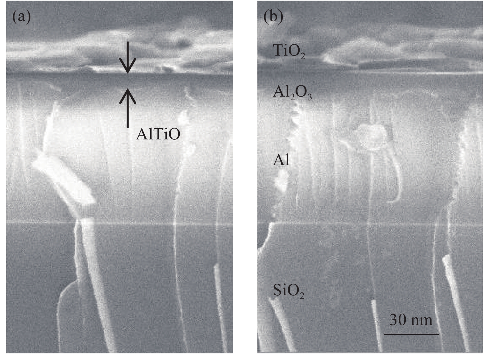
Fig. 1.
SEM cross section image of anodized region before top elec-trode deposition. (a) Sample 1 (AV = 25 V). (b) Sample 2 (AV = 30 V).
SEMICONDUCTOR MATERIALS
Corresponding author: R Karthik, Email: rayam16@gmail.com
Abstract: This paper presents the fabrication and modeling for capacitance–voltage characteristics of multi-layer metal–insulator–metal capacitors. It is observed that, due the applied electric field, the effective dielectric constant of the stack was increased due to the accumulation of charges at the interface of high-to-low conductance materials. It is observed that the Maxwell–Wagner polarization is dominant at low frequencies (<10 kHz). By introducing carrier tunneling probability of the dielectric stack, the model presented in this paper shows a good agreement with experimental results. The presented model indicates that the nonlinearity can be suppressed by choosing the similar permittivity dielectric materials for fabrication of multilayer metal insulator metal capacitors.
Keywords: anodic oxidation, dielectric, high-k, multi-layer, capacitance-voltage, Maxwell-Wagner, capacitor
| [1] |
He Z X, Daley D, Bolam R, et al. High and low density complimentary MIM capacitors fabricated simultaneously in advanced RFCMOS and BiCMOS technologies. IEEE Bipolar/BiCMOS Circuits Tech Meet, 2008: 212
|
| [2] |
Ding S J, Zhu C X, Li M F. Atomic-layer-deposited Al2O3-HfO2-Al2O3 dielectrics for metal-insulator-metal capacitor applications. Appl Phys Lett, 2005, 87: 053501 doi: 10.1063/1.2005397
|
| [3] |
Ding S J, Xu J, Zhang D W, et al. Electrical characteristics and conduction mechanisms of metal-insulator-metal capacitors with nanolaminated Al2O3-HfO2 dielectrics. Appl Phys Lett, 2008, 93: 092909 doi: 10.1063/1.2969399
|
| [4] |
Zhu B, Liu W J, Wei L, et al. Voltage-dependent capacitance behavior and underlying mechanisms in metal-insulator-metal capacitors with Al2O3-ZrO2-SiO2 nano-laminates. J Phys D, 2016, 49: 135106 doi: 10.1088/0022-3727/49/13/135106
|
| [5] |
Sillars R W. The properties of a dielectric containing semiconducting particles of various shapes. J Inst Elect Eng, 1937: 378
|
| [6] |
Ge S B, Shen M R, Ning Z Y. Dielectric enhancement and Maxwell Wagner effect in polycrystalline BaTiO3Ba0.2Sr0.8TiO3 multilayered thin films. Chin Phys Lett, 1996, 19(4): 563
|
| [7] |
Qu B D, Evstigneev M, Johnson D J, et al. Dielectric properties of BaTiO3/SrTiO3 multilayered thin films prepared by pulsed laser deposition. Appl Phy Lett, 1998, 1394
|
| [8] |
O'Neill D, Bowman R M, Gregg J M, et al. Dielectric enhancement and Maxwell-Wagner effects in ferroelectric superlattice structures. Appl Phy Lett, 2000, 77: 1520 doi: 10.1063/1.1290691
|
| [9] |
Catalan G, O'Neill D, et al. Relaxor features in ferroelectric superlattices: A Maxwell-Wagner approach. Appl Phys Lett, 2000, 77: 3078 doi: 10.1063/1.1324729
|
| [10] |
Shen M, Ge S, Cao W, et al. Dielectric enhancement and Maxwell-Wagner effects in polycrystalline ferroelectric multilayered thin films. J Phy D, 2001, 34 (19): 2935 doi: 10.1088/0022-3727/34/19/301
|
| [11] |
Li W, Auciello O, Premnath R N, et al. Giant dielectric constant dominated by Maxwell-Wagner relaxation in Al2O3/TiO2 nanolaminates synthesized by atomic layer deposition. Appl Phys Lett, 2010, 96: 162907 doi: 10.1063/1.3413961
|
| [12] |
Jinesh K B, Lamy Y, Klootwijk J H, et al. Maxwell-Wagner instability in bilayer dielectric stacks. Appl Phy Lett, 2009, 95: 122903 doi: 10.1063/1.3236532
|
| [13] |
Karthik R, Kannadassan D, Baghini M S, et al. Nanostructured Bilayer Anodic TiO2/Al2O3 Metal-Insulator-Metal capacitor. J Nanosci Nanotech, 2013, 13: 1 doi: 10.1166/jnn.2013.6733
|
| [14] |
Sze S M, Ng Kwok K. Physics of semiconductor devices. John Wiley & Sons, 2006
|
| [15] |
Maxwell J C. A treatise on electricity and magnetism. Oxford: Clarendon Press, 1873
|
| [16] |
Morshuis P H F, Bodega R, Fabiani D, et al. Dielectric interfaces in dc constructions: Space charge and polarization phenomena. IEEE International Conference on Solid Dielectrics, ICSD, 2007, 450
|
| [17] |
Houssa M, Tuominen M, Naili M, e t al. Trap-assisted tunneling in high permittivity gate dielectric stacks. J Appl Phys, 2000, 87(12): 8615 doi: 10.1063/1.373587
|
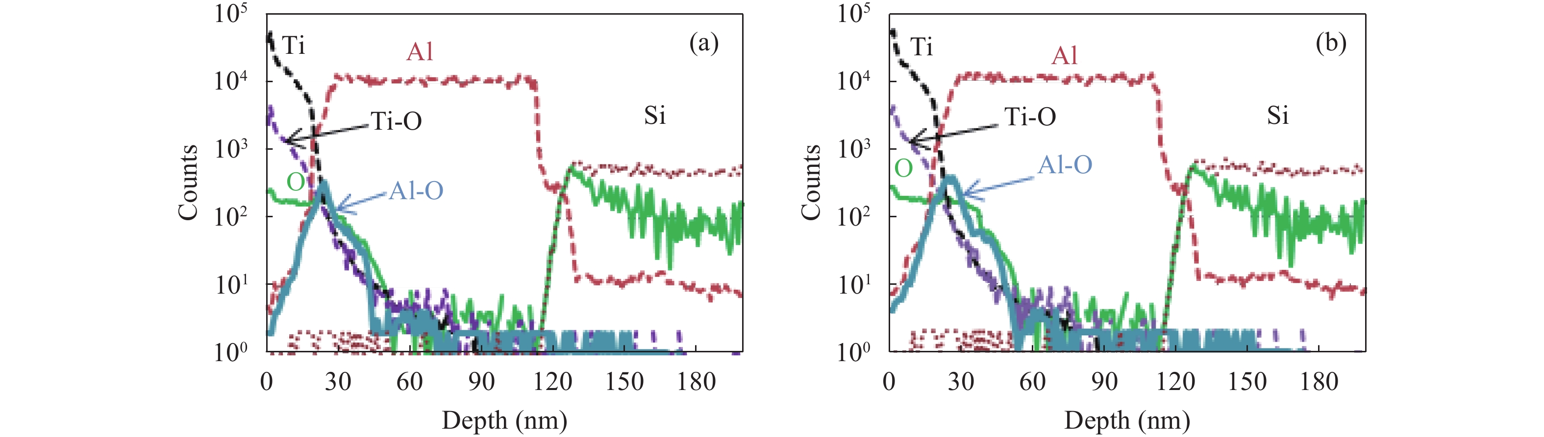
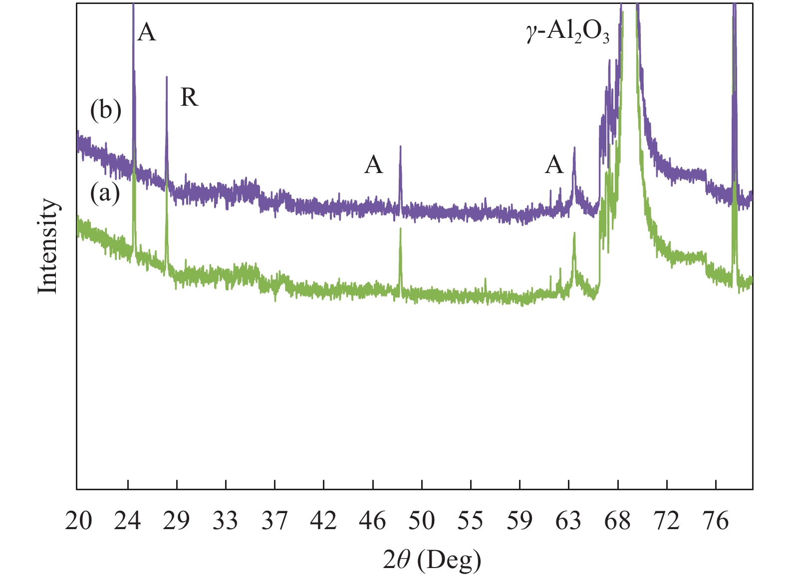
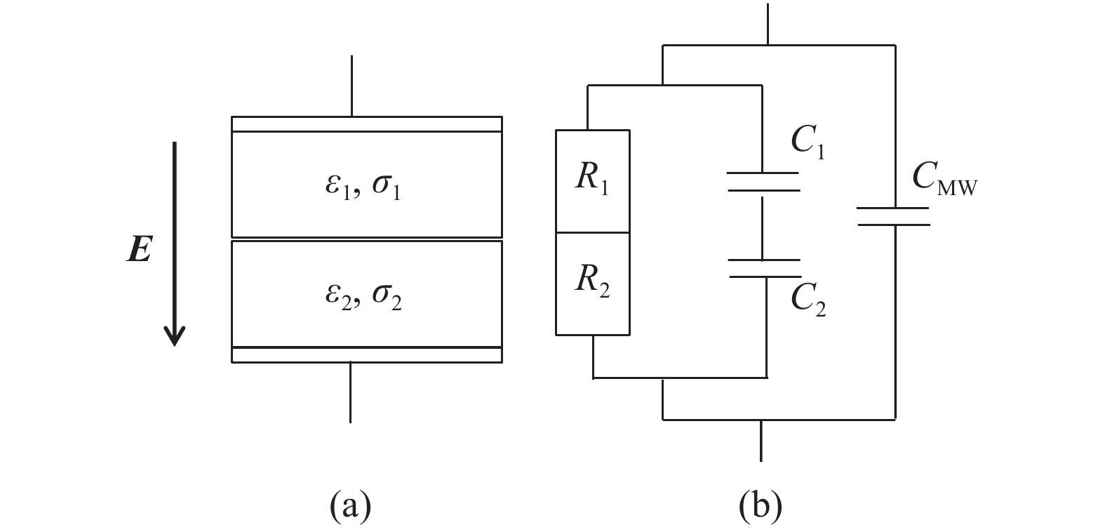
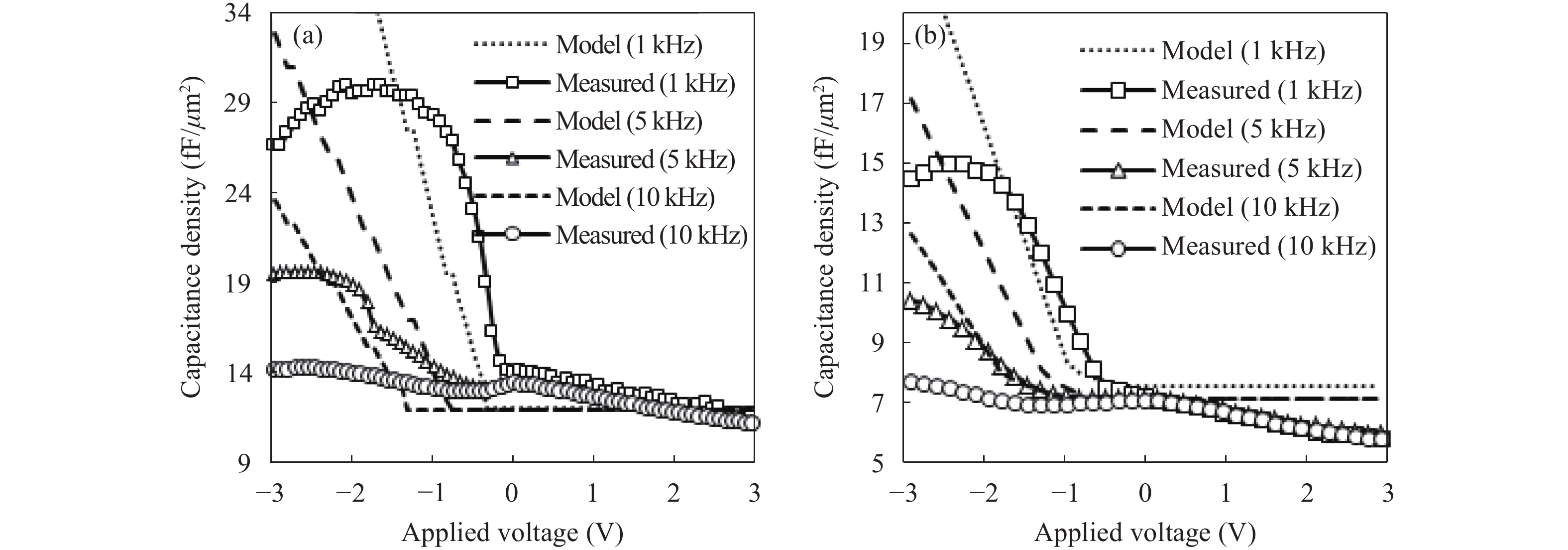
Table 1. Fitting parameters of Maxwell–Wagner capacitance model.
| Sample | d1 (nm) | d2 (nm) | εr1 | εr2 | σ1 (pS/cm) | σ2 (fS/cm) | Φ1 (eV) | Φ2 (eV) | Vbi (eV) |
| Sample 1 | 15 | 7 | 90 | 9 | 15 | 2 | 3.3 | 2.3 | 1 |
| Sample 2 | 15 | 10 | 90 | 9 | 15 | 4 | 3.3 | 2.3 | 1.2 |
 DownLoad: CSV
| [1] |
He Z X, Daley D, Bolam R, et al. High and low density complimentary MIM capacitors fabricated simultaneously in advanced RFCMOS and BiCMOS technologies. IEEE Bipolar/BiCMOS Circuits Tech Meet, 2008: 212
|
| [2] |
Ding S J, Zhu C X, Li M F. Atomic-layer-deposited Al2O3-HfO2-Al2O3 dielectrics for metal-insulator-metal capacitor applications. Appl Phys Lett, 2005, 87: 053501 doi: 10.1063/1.2005397
|
| [3] |
Ding S J, Xu J, Zhang D W, et al. Electrical characteristics and conduction mechanisms of metal-insulator-metal capacitors with nanolaminated Al2O3-HfO2 dielectrics. Appl Phys Lett, 2008, 93: 092909 doi: 10.1063/1.2969399
|
| [4] |
Zhu B, Liu W J, Wei L, et al. Voltage-dependent capacitance behavior and underlying mechanisms in metal-insulator-metal capacitors with Al2O3-ZrO2-SiO2 nano-laminates. J Phys D, 2016, 49: 135106 doi: 10.1088/0022-3727/49/13/135106
|
| [5] |
Sillars R W. The properties of a dielectric containing semiconducting particles of various shapes. J Inst Elect Eng, 1937: 378
|
| [6] |
Ge S B, Shen M R, Ning Z Y. Dielectric enhancement and Maxwell Wagner effect in polycrystalline BaTiO3Ba0.2Sr0.8TiO3 multilayered thin films. Chin Phys Lett, 1996, 19(4): 563
|
| [7] |
Qu B D, Evstigneev M, Johnson D J, et al. Dielectric properties of BaTiO3/SrTiO3 multilayered thin films prepared by pulsed laser deposition. Appl Phy Lett, 1998, 1394
|
| [8] |
O'Neill D, Bowman R M, Gregg J M, et al. Dielectric enhancement and Maxwell-Wagner effects in ferroelectric superlattice structures. Appl Phy Lett, 2000, 77: 1520 doi: 10.1063/1.1290691
|
| [9] |
Catalan G, O'Neill D, et al. Relaxor features in ferroelectric superlattices: A Maxwell-Wagner approach. Appl Phys Lett, 2000, 77: 3078 doi: 10.1063/1.1324729
|
| [10] |
Shen M, Ge S, Cao W, et al. Dielectric enhancement and Maxwell-Wagner effects in polycrystalline ferroelectric multilayered thin films. J Phy D, 2001, 34 (19): 2935 doi: 10.1088/0022-3727/34/19/301
|
| [11] |
Li W, Auciello O, Premnath R N, et al. Giant dielectric constant dominated by Maxwell-Wagner relaxation in Al2O3/TiO2 nanolaminates synthesized by atomic layer deposition. Appl Phys Lett, 2010, 96: 162907 doi: 10.1063/1.3413961
|
| [12] |
Jinesh K B, Lamy Y, Klootwijk J H, et al. Maxwell-Wagner instability in bilayer dielectric stacks. Appl Phy Lett, 2009, 95: 122903 doi: 10.1063/1.3236532
|
| [13] |
Karthik R, Kannadassan D, Baghini M S, et al. Nanostructured Bilayer Anodic TiO2/Al2O3 Metal-Insulator-Metal capacitor. J Nanosci Nanotech, 2013, 13: 1 doi: 10.1166/jnn.2013.6733
|
| [14] |
Sze S M, Ng Kwok K. Physics of semiconductor devices. John Wiley & Sons, 2006
|
| [15] |
Maxwell J C. A treatise on electricity and magnetism. Oxford: Clarendon Press, 1873
|
| [16] |
Morshuis P H F, Bodega R, Fabiani D, et al. Dielectric interfaces in dc constructions: Space charge and polarization phenomena. IEEE International Conference on Solid Dielectrics, ICSD, 2007, 450
|
| [17] |
Houssa M, Tuominen M, Naili M, e t al. Trap-assisted tunneling in high permittivity gate dielectric stacks. J Appl Phys, 2000, 87(12): 8615 doi: 10.1063/1.373587
|


Article views: 4464 Times PDF downloads: 69 Times Cited by: 0 Times
Received: 24 March 2017 Revised: 05 May 2017 Online: Published: 01 December 2017
| Citation: |
R Karthik, A Akshaykranth. Fabrication and modeling of multi-layer metal–insulator-metal capacitors[J]. Journal of Semiconductors, 2017, 38(12): 123002. doi: 10.1088/1674-4926/38/12/123002
****
R Karthik, A Akshaykranth. Fabrication and modeling of multi-layer metal–insulator-metal capacitors[J]. J. Semicond., 2017, 38(12): 123002. doi: 10.1088/1674-4926/38/12/123002.

|
| [1] |
He Z X, Daley D, Bolam R, et al. High and low density complimentary MIM capacitors fabricated simultaneously in advanced RFCMOS and BiCMOS technologies. IEEE Bipolar/BiCMOS Circuits Tech Meet, 2008: 212
|
| [2] |
Ding S J, Zhu C X, Li M F. Atomic-layer-deposited Al2O3-HfO2-Al2O3 dielectrics for metal-insulator-metal capacitor applications. Appl Phys Lett, 2005, 87: 053501 doi: 10.1063/1.2005397
|
| [3] |
Ding S J, Xu J, Zhang D W, et al. Electrical characteristics and conduction mechanisms of metal-insulator-metal capacitors with nanolaminated Al2O3-HfO2 dielectrics. Appl Phys Lett, 2008, 93: 092909 doi: 10.1063/1.2969399
|
| [4] |
Zhu B, Liu W J, Wei L, et al. Voltage-dependent capacitance behavior and underlying mechanisms in metal-insulator-metal capacitors with Al2O3-ZrO2-SiO2 nano-laminates. J Phys D, 2016, 49: 135106 doi: 10.1088/0022-3727/49/13/135106
|
| [5] |
Sillars R W. The properties of a dielectric containing semiconducting particles of various shapes. J Inst Elect Eng, 1937: 378
|
| [6] |
Ge S B, Shen M R, Ning Z Y. Dielectric enhancement and Maxwell Wagner effect in polycrystalline BaTiO3Ba0.2Sr0.8TiO3 multilayered thin films. Chin Phys Lett, 1996, 19(4): 563
|
| [7] |
Qu B D, Evstigneev M, Johnson D J, et al. Dielectric properties of BaTiO3/SrTiO3 multilayered thin films prepared by pulsed laser deposition. Appl Phy Lett, 1998, 1394
|
| [8] |
O'Neill D, Bowman R M, Gregg J M, et al. Dielectric enhancement and Maxwell-Wagner effects in ferroelectric superlattice structures. Appl Phy Lett, 2000, 77: 1520 doi: 10.1063/1.1290691
|
| [9] |
Catalan G, O'Neill D, et al. Relaxor features in ferroelectric superlattices: A Maxwell-Wagner approach. Appl Phys Lett, 2000, 77: 3078 doi: 10.1063/1.1324729
|
| [10] |
Shen M, Ge S, Cao W, et al. Dielectric enhancement and Maxwell-Wagner effects in polycrystalline ferroelectric multilayered thin films. J Phy D, 2001, 34 (19): 2935 doi: 10.1088/0022-3727/34/19/301
|
| [11] |
Li W, Auciello O, Premnath R N, et al. Giant dielectric constant dominated by Maxwell-Wagner relaxation in Al2O3/TiO2 nanolaminates synthesized by atomic layer deposition. Appl Phys Lett, 2010, 96: 162907 doi: 10.1063/1.3413961
|
| [12] |
Jinesh K B, Lamy Y, Klootwijk J H, et al. Maxwell-Wagner instability in bilayer dielectric stacks. Appl Phy Lett, 2009, 95: 122903 doi: 10.1063/1.3236532
|
| [13] |
Karthik R, Kannadassan D, Baghini M S, et al. Nanostructured Bilayer Anodic TiO2/Al2O3 Metal-Insulator-Metal capacitor. J Nanosci Nanotech, 2013, 13: 1 doi: 10.1166/jnn.2013.6733
|
| [14] |
Sze S M, Ng Kwok K. Physics of semiconductor devices. John Wiley & Sons, 2006
|
| [15] |
Maxwell J C. A treatise on electricity and magnetism. Oxford: Clarendon Press, 1873
|
| [16] |
Morshuis P H F, Bodega R, Fabiani D, et al. Dielectric interfaces in dc constructions: Space charge and polarization phenomena. IEEE International Conference on Solid Dielectrics, ICSD, 2007, 450
|
| [17] |
Houssa M, Tuominen M, Naili M, e t al. Trap-assisted tunneling in high permittivity gate dielectric stacks. J Appl Phys, 2000, 87(12): 8615 doi: 10.1063/1.373587
|

 WeChat ID
Journal of Semiconductors © 2017 All Rights Reserved 京ICP备05085259号-2


