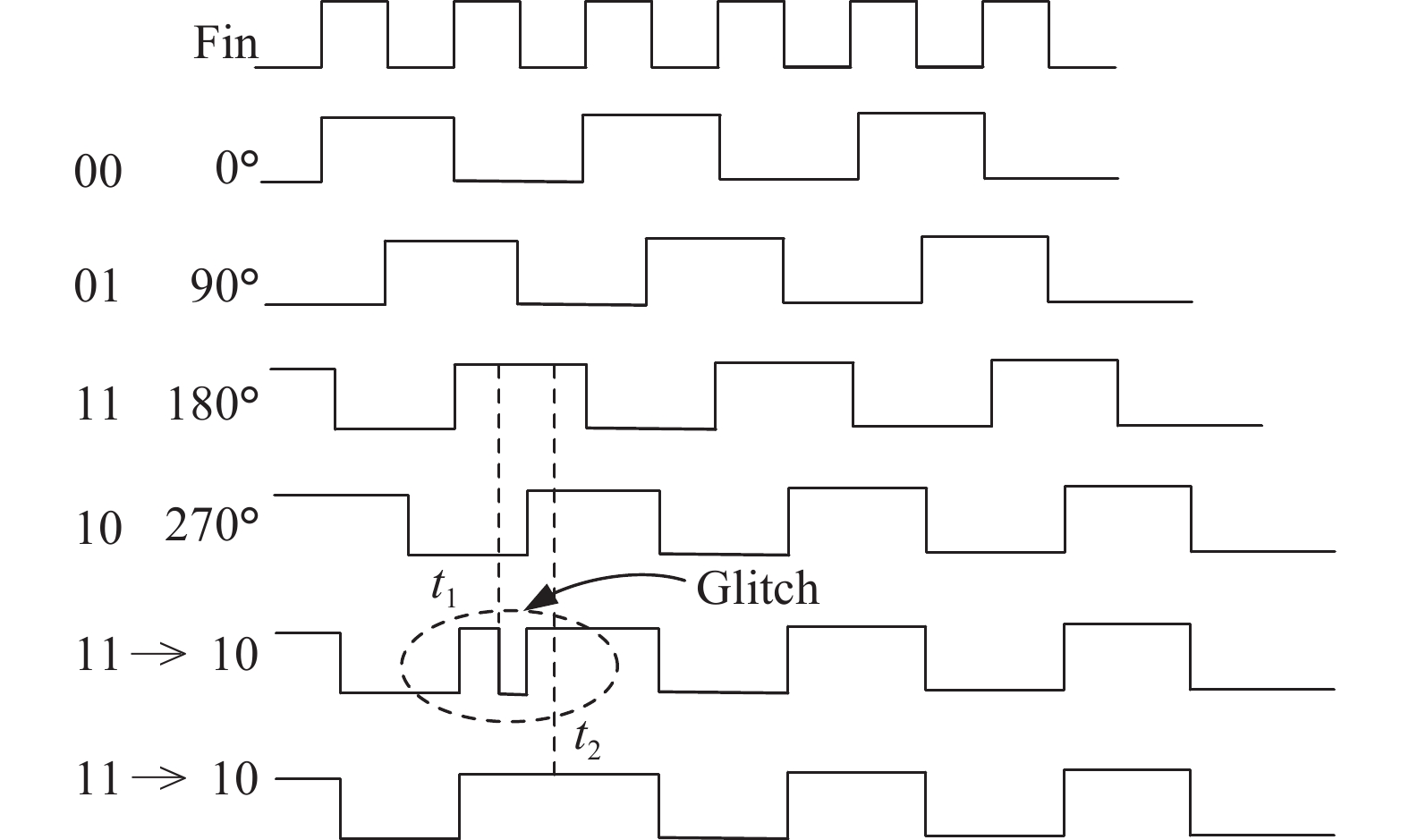
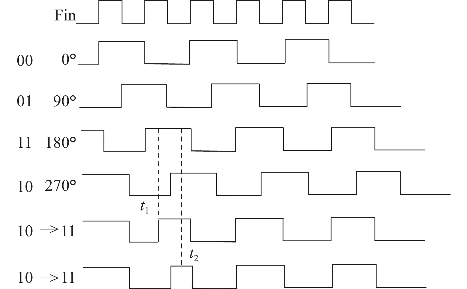
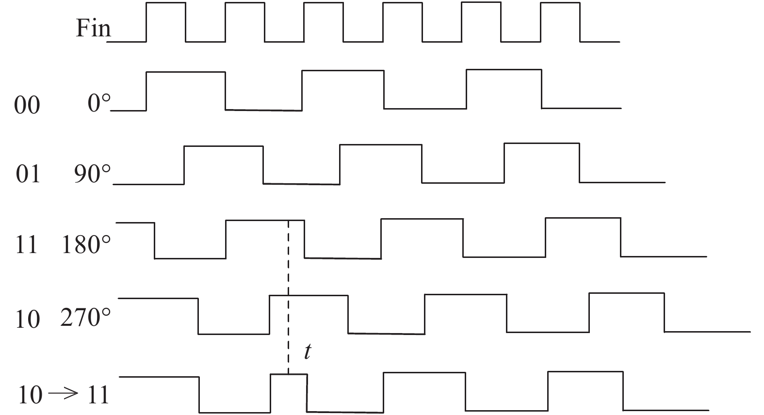
Processing math: 100%
J. Semicond. > 2017, Volume 38 > Issue 12 > 125001

SEMICONDUCTOR INTEGRATED CIRCUITS

A fractional-N frequency divider for multi-standard wireless transceiver fabricated in 0.18 μm CMOS process

Jiafeng Wang, Xiangning Fan, Xiaoyang Shi and Zhigong Wang

+ Author Affiliations

 Corresponding author: gdqs008@163.com, 736362442@qq.com

DOI: 10.1088/1674-4926/38/12/125001

PDF

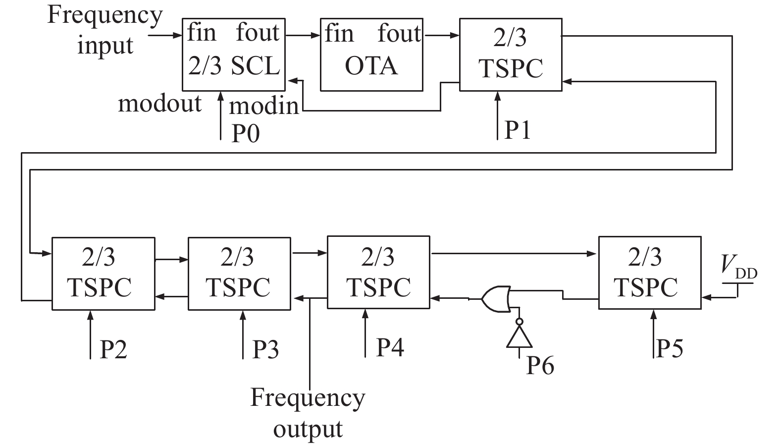
Abstract: With the rapid evolution of wireless communication technology, integrating various communication modes in a mobile terminal has become the popular trend. Because of this, multi-standard wireless technology is one of the hot spots in current research. This paper presents a wideband fractional-N frequency divider of the multi-standard wireless transceiver for many applications. High-speed divider-by-2 with traditional source-coupled-logic is designed for very wide band usage. Phase switching technique and a chain of divider-by-2/3 are applied to the programmable frequency divider with 0.5 step. The phase noise of the whole frequency synthesizer will be decreased by the narrower step of programmable frequency divider. Δ–Σ modulator is achieved by an improved MASH 1-1-1 structure. This structure has excellent performance in many ways, such as noise, spur and input dynamic range. Fabricated in TSMC 0.18μm CMOS process, the fractional-N frequency divider occupies a chip area of 1130 × 510 μm2 and it can correctly divide within the frequency range of 0.8–9 GHz. With 1.8 V supply voltage, its division ratio ranges from 62.5 to 254 and the total current consumption is 29 mA.

Key words: multi-standardfrequency synthesizerfractional-N frequency dividerphase switchingΔ–Σ modulator

Wireless communication systems and corresponding services are developing quickly over the whole world. The advanced 3G technology 3GPP-LTE has been applied in our lifetime. At present, the satellite navigation system BEIDOU developed by China can work successfully with other systems like GPS, GLONASS and GALILEO. It is already beginning to provide navigation services to China and near countries recently. Except short distance communication, the wireless sensor network based on IEEE 802.15.4 and the IOT (internet of things) have great value in industry, military and other fields[1]. WLAN (wireless local area network) also has great prospects in high-speed wireless communication.

With the rapid development of wireless communication modes and communication terminals, integrating various communication modes in a mobile terminal has become the trend of the wireless communication technology[2, 3]. Because of this, the multi-standard wireless transceiver is one of the hot spots in current research. As the key part, a frequency synthesizer determines the performance and integration level of the wireless transceiver. The frequency synthesizer can output multiple frequency signals with high precision by changing the frequency division of fractional-N frequency divider. So the fractional-N frequency divider is very important to the system.

A fractional-N frequency divider is composed of a programmable frequency divider and a Δ–Σ modulator. As a very important factor, phase noise influences the performance of the whole transceiver. The technology to restrain phase noise is being used in lots of structures. Compared with conventional structure, reducing the division ratio interval is a good way to decrease the phase noise. This thesis uses phase switching technology and a chain of divider-by-2/3 to realize a programmable frequency divider with 0.5 step which reduces the phase noise of the whole loop. A high-speed divider-by-2 with traditional source-coupled-logic is designed for very wide band usage. Phase switching technique and a chain of divider-by-2/3 are applied to the programmable frequency divider with 0.5 step. The phase noise of the whole frequency synthesizer will be decreased by the narrower step of programmable frequency divider. Δ–Σ modulator is achieved by an improved MASH 1-1-1 structure.

The whole fractional-N frequency divider is implemented in TSMC 0.18 μm RF CMOS process, occupying a chip area of 1130 × 510 μm2. With 1.8 V supply voltage and 29 mA current consumption, the measurement results show that it can correctly divide within the frequency range of 0.8–9 GHz and its division ratio ranges from 62.5 to 254.

In the Δ-Σ fractional-N frequency synthesizer, the output phase noise generated by quantization noise of Δ-Σ modulator can be described as follows[4]:

SΔ(f)=fref|HΔ(f)|2|Hdiv(f)|2Δ212,

In this formula, fref is the reference frequency, HΔ(f) is the quantization noise transfer function of Δ-Σ modulator, Hdiv(f) is the phase noise transfer function of divider and is division ratio interval, SΔ(f) is the power spectral density of phase noise generated by quantization noise.

Quantization noise is the main spur in Δ–Σ fractional-N frequency synthesizer. It affects the whole performance of the frequency synthesizer. From formula (2.1), lower fref and lower loop-bandwidth can decrease the influence of quantization noise, but 1/f flicker noise and phase noise of VCO will increase at the same time. Reducing the division ratio interval Δ is a good way to decrease the quantization noise without affecting other modules. The output phase noise will have 6 dB improvement when Δ interval reduces 0.5. This design uses a programmable frequency divider with 0.5 step.

The most important thing to design a programmable frequency divider with 0.5 step is to design an N/N+0.5 dual-module pre-scaler. Two structures will be considered to complete an N/N+0.5 dual-module pre-scaler. The first is bilateral trigger structure and the other is phase switching structure[4].

Bilateral flip-flop can work well at low frequency, but it does not adapt to high frequency due to its sensitivity to circuit delay. Phase switching structure has low power consumption and excellent reliability. What is more, it can work well at a high frequency. This paper uses phase switching architecture to design a programmable frequency divider with 0.5 step.

Figure  1.  Waveform of phase switching.

The phase switching waveform is shown in Fig. 1. The first line is clock signal and the next four signals are orthogonal signals whose frequency is half of the clock signal. They are generated by high-speed divider-by-two and are indicated as 00 (0°), 01 (90°), 11 (180°), 10 (270°). Just one of them will be selected at any time. In Fig. 1, the waveform of output signal is switched from 10 to 11 at time t and the output signal swallows 1/4 period. In other words, it swallows 1/2 period of the clock signal. Controlling the times of switching can achieve 1 and 1.5 step.

Phase switching is a good method but there is an obvious shortcoming. Glitch is a serious weakness in phase switching technology. In Fig. 2, no glitch appears when switching happens at time t2, but when switching happens at time t1, the glitch cannot be ignored. It generates an extra rising edge.

Figure  2.  Influence of glitch.

Lots of methods can be used to eliminate the influence of glitch and forward-switching is the most efficient and simplest method[5]. Output signal is switched from 10 forward to 11 in Fig. 3. Different from Fig. 2, no glitch appears when switching happens at time t1 or t2. The most important thing of forward-switching is that the target signal must be high level ‘1’ when the rising edge of current signal comes. Because level ‘1’ changed to level ‘1’ or level ‘0’ changed to level ‘0’ will not generate extra edges. Similarly, level ‘0’ changed to level ‘1’ just forwards of the rising edge. But level ‘1’ changed to level ‘0’ is not a safe change. An extra edge will be generated when the rising edge of the target signal is a little behind the switching time. Forward-switching technique can faultlessly solve this problem.

Figure  3.  Forward-switching with no glitch.
Figure  4.  (Color online) Block diagram of the frequency synthesizer.
Figure  5.  Structure of the fractional-N frequency divider.

The multi-standard fractional-N frequency divider designed by this thesis is applied for wireless communications, satellite navigation, wireless sensor network and other applications. It will face lots of challenges compared to the common ones. The biggest difficulty of this thesis is to realize almost all communication standards and the frequency synthesizer need to make output frequency range 0.7–3.8 GHz. If the frequency synthesizer is designed in double structure (it generates two times the frequency of the local signal), the voltage control oscillator (VCO) must let output frequency range be 1.4–7.6 GHz. It is very difficult to design such a VCO because this frequency synthesizer is fabricated in TSMC 0.18μm RF CMOS process. This thesis uses two VCOs to achieve 1.4–7.6 GHz output frequency range. The higher VCO covers 4–7.6 GHz and the lower one covers 1.4–4 GHz.Fig. 4 presents the structure diagram of the fractional-N frequency synthesizer.

The whole structure of the fractional-N frequency divider is displayed in Fig. 5. It consists of a high-speed divider-by-2, a programmable frequency divider with 0.5 step and a Δ–Σ modulator. The output signal of VCO goes through the first high-speed divider-by-2 and becomes four quadrature signals. These four quadrature signals are the output of frequency synthesizer and then they will be provided into the later mixer. Furthermore, the programmable frequency divider with 0.5 step is composed of a high-speed divider-by-2 which follows the first one, a phase switching circuit, an integer-N programmable frequency divider and a logic control module. Δ–Σ modulator is achieved by an improved MASH 1-1-1 structure. It changes the control words P0-P8 to make the real-time division ratio random.

A divider-by-2 can be simply completed by a D flip-flop that is made up of a master and a slave digital latch. SCL (source coupled logic) latch has very high working frequency, bandwidth and satisfactory quadrature performance. Therefore it is suitable for high-speed divider-by-2. The schematic of divider-by-2 with SCL logic is shown in Fig. 6. The trail-transistor provides constant current to hold the output swing and positive feedback is formed by connecting its output ports back to its input ports.

Figure  6.  High speed divider-by-2 based on SCL logic.

A clock divider can be best characterized by its sensitivity curve, which gives the requested minimum amplitude Vmin of the input signal[6]. A typical sensitivity curve is presented in Fig. 7.

In region I, the divider is locked to the half-rate frequency. This function is the intended operation of the circuit. Self-oscillation frequency (fso) is also an important parameter. Requirement for the amplitude of input signal will be the least when its frequency equals to double self-oscillation frequency. The amplitude requirement will be higher when the input frequency is farther from 2fso because the slope after 2fso is higher than the prior one. Thus, making 2fso be slightly lower than fin, max is a common robust design method. In fact, the IC process and temperature will bring significant influence on fso. These effects should be considered by circuit designers.

Figure  7.  Sensitivity curve of SCL structure.

In this design, the structure of tail current transistor with resistance load is used for constant current and invariant output swing. Compared with the MOS load, the area of resistance load is larger and temperature always influences it. But the parasitic capacitance of resistance load is small, which is quite necessary to improve the working frequency of the divider-by-2. Layout technique and adding dummy are two considerable methods to decrease the impact of temperature.

With the resistance load, the maximum and minimum output voltage is VDD and VDD-IssR, Iss in this equation indicates the bias current of trail-transistor. Generally speaking, the average output voltage equals to (1/2)IssR. Basic circuit theory indicates that the conversion rate of a circuit must be larger than V0W0 if it amplifies a signal V0 sin(w0t + θ) so that following equation can be easily acquired[7]:

IssCLV0ω0=12IssR×2πf0,

(2)

R1πf0CL,

(3)

CL in Eq. (2) is the load capacitance at the output port and f0 represents the frequency of output signal. The load resistance R is generally set as the maximum value for the lowest power consumption. Iss can be easily obtained according to the request of output swing. The constraint formula of positive feedback is shown as follows:

gm5/m6R1.

(4)

Similarly, the gm5 and gm6 are usually set as the minimum value for the lowest power consumption so that the current of latch branch is:

I2=12gm5Von+12gm6Von=gm5/m6Von.

(5)

The current of sample branch is:

I1=IssI2.

(6)

From the above analysis, the parameters of each transistor can be calculated in theory[8].

The circuit for phase switching is shown in Fig. 8. The input of divider-by-2 is equal to the output of PLL and its frequency ranges from 0.5 to 4 GHz. The input signal goes through divider-by-2 and turns into four quadrature signals. The phase switching circuit is made up of two common source amplifiers and a 4-1 transfer-gate multiplexer. The selected signal goes through a common source buffer to the later circuits. The common source amplifier is suited for dealing with differential signals and it can compensate the attenuation of transfer-gate.

The difficulty of this design is setting the parameters of transistors. The output of divider-by-2 will be selected after a common source amplifier. Theoretically speaking, the highest frequency in phase switching circuit is 2 GHz. In fact, the waveform after switching is not a 2 GHz sine wave, but a complex wave within 2 GHz sine wave and harmonic wave. The common source buffer needs to reshape this irregular wave to the later circuit. The bandwidth of system will have a large drop due to the influence of parasitic effect in post-simulation. Therefore, the common source amplifier should be good at dealing with a wide band harmonic wave. Because of the contradiction of gain and bandwidth, it is important to take both of them into account.

Figure  8.  Structure of phase switching.

The integer-N programmable frequency divider is based on a chain of divider-by-2/3. The divider-by-2/3 cell as shown in Fig. 10 will be divided by 3 when the control signals P and modin are both high. In the other case, it will be divided by 2.

The integer-N programmable frequency divider operates as follows: the enable control signal modin(n) on the last cell will be set as effective all the time and modin(n-1) is the output signal of the last cell. For the divider-by-2/3, division by 3 will increase an extra period to the corresponding cell[9]. So the division ratio of the programmable frequency divider can be described by the following:

M=P0+2P1+22P2+...+2n1Pn1+2n.

(7)

Eq. (6) makes the division ratio of integer-N programmable divider range from 2n (ALL Pn = 0) to 2n+1−1 (ALL Pn = 1). It is not wide enough for the multi-standard application so that extending the division ratio range is necessary. Adding some logic gates in the chain is an appropriate way to make this improvement come true. The block diagram is displayed in Fig. 9.

The logic OR gate is invisible to the whole system when the control port P6 = 1 and the division ratio ranges from 26 to 27−1. When P6 = 0, the last divider will be disabled and the division ratio range is changed to 25−26−1. In a word, the whole division ratio range has been extended to 25−27−1 by controlling P6.

The first divider still uses SCL structure to deal with high frequency and the circuit diagram is described in depth in Fig. 10. It consists of a pre-scaler logic, an end-of-cycle logic and several AND gates[10]. Generally speaking, AND gate is always achieved by CMOS combination. CMOS combination cannot deal with high frequency smoothly due to its high gate delay. More transistors of traditional CMOS combination result in the increase of layout area[11]. Integrating AND gates into the SCL structure is an ideal way to solve the problems above. Fig. 11 gives the specific circuit diagram.

Figure  9.  Structure of integer-N programmable divider.
Figure  10.  Block diagram of divider-by-2/3.

The frequency will get down to 1GHz after the first divider-by-2/3 and traditional digital flip-flops can work at this frequency. Therefore, TSPC structure is used except the first divider-by-2/3. As in Fig. 11, logic gates can be integrated into TSPC structure to reduce area consumption. The boundary between analog and digital signals is after the first divider-by-2/3. There is a trans-conductance amplifier (OTA) which is used to change the weak differential signals to a single-ended rail-to-rail signal[7].

The logic control module is used to select phase switching times. As shown in Fig. 12, the input signal of logic control module is from integer-N programmable divider. The trans-conductance amplifier in integer-N programmable divider provides the clock signal. A new period begins when the drop edge comes. Then the pulse generator produces a short pulse as a clean signal to make the counter be ‘0’ state. The counter and gray state machine will work once when a rise edge of CLK signal comes. The counter will work continually until its output equals to P0P1. EN signal makes the logic control module static until a new period comes.

Figure  11.  SCL with AND gate.

The digital Δ–Σ modulator (DDSM) is the key part of this circuit. Three important factors of DDSM are listed as follows[12]. The first one is the accuracy of the output sequence. It is requested that the average of the output sequence must equal to the input signal accurately. The second one is the length of the output sequence. It must be long enough to decrease the influence of fractional-N spur in PLL. The last one is dynamic input range. From the target requirement, the input signal of DDSM must be set as any integer between 0 to 2N−1, N is the bit length of input.

Figure  12.  Logic control module.

The structure of improved MASH 1-1-1 DDSM is presented in Fig. 13. Compared to conventional DDSM, its EFM (error feedback modulator) has two inputs. Except previous quantization error signal ei[n], the output signal of previous circuit will be sent to later blocks simultaneously[13]. When the input signal is constant, the length of the output of improved DDSM equals to N1M2 regardless of the initial value. In this equation, N1 is the output signal’s length of the first EFM and M is the bit length of EFM[14].

Figure  13.  Structure of improved MASH 1-1-1 DDSM.

The fractional-N frequency divider with phase switching technique for multi-standard wireless transceiver is fabricated in TSMC 0.18 μm RF CMOS process. It occupies a chip area of 1130 × 510 μm2 and Fig. 14 provides the chip photo of this frequency divider.

Figure  14.  (Color online) Chip photo of the frequency divider.

Independent simulation and combined simulation are both necessary due to the wideband working frequency. It is also important to make adjustment with circuit and layout according to the post-simulation results. Self-oscillation frequency and input sensitivity are important parameters of the high speed divider-by-two. Both of them represent the least power needed by the system under the working frequency range. The measurement results of self-oscillation frequency and input sensitivity are shown in Figs. 15 and 16. Through Fig. 15, the self-oscillation frequency of high-speed divider-by-two is 3.647 GHz. Fig. 16 indicates that the input power needed is least near 7.5 GHz, which equals to double self-oscillation frequency of high-speed divider-by-two. Furthermore, the circuit can work correctly at 1–8 GHz only when the power of input signal is bigger than −12 dBm.

Figure  15.  (Color online) Test result of self-oscillation frequency.
Figure  16.  (Color online) Measurement result of input sensitivity.

Make the Δ–Σ modulator free and set the input signal to the highest working frequency as 8 GHz sine signal. Then make the control words 1101_0000_1 and its theoretical division ratio is 130.5. The spectrum of the measurement result is indicated in Fig. 17. It is easy to get the correct division ratio from Fig. 17 and the measurement result shows that the whole system works correctly. In a similar testing way, Fig. 18 is the spectrum generated by division ratio 67.

Figure  17.  (Color online) Spectrum without Δ-Σ modulator.
Figure  18.  (Color online) Spectrum generated by division ratio 67.

Because of the changing division ratio, the spectrum of output signal is changing ceaselessly. The average function of spectrum analyzer can be used to test the spectrum when the Δ-Σ modulator is working. Set the input signal as 8 GHz sine signal and make the division ratio of programmable frequency divider with 0.5 step to 67.5. The input of Δ-Σ modulator is set as 20b’1000_0000_0000_0000_0000 for easy testing. The theoretical division ratio of the whole circuit is 67.75. From the average spectrum of the fractional-N frequency divider in Fig. 19, the entire system with Δ-Σ modulator works correctly.

Figure  19.  (Color online) Average spectrum with Δ-Σ modulator.

Table 1 presents the comparison between simulation results, measurement results and design index. The measured performance of this fractional-N frequency divider and other recently published wideband frequency dividers are summarized in Table 2. Compared with other designs, this work has a very wide band to realize multi-standard for almost all communication modes. Obviously, its wide band is at the expense of relatively high power consumption.

Table  1.  Comparison between simulation results, measurement results and design index.
Parameter Design index Pre-simulation results Post-simulation results Measurement results
Working frequency (GHz) 1–8 0.5–9.7 0.5–9 0.5–9
Current (mA) <35 <29.7 <30.03 29
Division ratio 70–200 62.5–254 62.5–254 62.5–254
Output swing (V) 0–1.8 0–1.8 0–1.8 0–1.8
DownLoad: CSV  | Show Table
Table  2.  Summary and performance comparison.
Reference Technology Technique Working frequency (GHz) Power consumption (mW) Division ratio Area (mm2)
This work 0.18 μm CMOS Phase switching 0.5–9 52.2 62.5–254 1.13 × 0.51
Ref. [15] 90 nm CMOS Direct injection-locked 27.2–42.3 3.6 2 0.5 × 0.5
Ref. [16] 0.7 μm InP DHBT ECL DFF 1–83 350 2 0.62×0.65
Ref. [17] 0.18 μm CMOS ECL DFF 1.1–2.5 1.98 8/9
Ref. [18] 1 μm InGap/GaAs Regenerative injection-locked 12–40 300.85 2 0.47 × 0.22
DownLoad: CSV  | Show Table

The phase noise of the frequency synthesizer is an important point of this design and the whole system has been finished recently. Fig. 20 shows that the phase noise is about −107 dBc/Hz at output frequency 5.68 GHz (@ 1 MHz). The measurement results meet the design target. Regrettably, digital power brings some bad influences to analog circuits, but post-simulation cannot indicate these changes accurately. Better isolation technique should be used for next design.

Figure  20.  (Color online) Phase noise of frequency synthesizer.

This paper presents a fractional-N frequency divider for multi-standard wireless transceiver. Phase switching technique is used to decrease the interval of Δ-Σ modulator for low phase noise. The whole fractional-N frequency divider is fabricated in TSMC 0.18 μm RF CMOS process, occupying a chip area of 1130 × 510 μm2. This chip can correctly divide within the frequency range of 0.8–9 GHz with 1.8 V supply voltage. The total current consumption is 29 mA and its division ratio ranges from 62.5 to 254. The wideband working frequency makes it comfortable for GPS, GSM, Galileo and other communication modes.


[1]
Brandolini M, Rossi P, Manstretta D, et al. Toward multistandard mobile terminals—fully integrated receivers requirements and architectures. IEEE Trans Microwave Theory Tech, 2005, 53(3): 1026 doi: 10.1109/TMTT.2005.843505
[2]
Shu K, Sánchez-Sinencio E. CMOS PLL synthesizers: analysis and design. Springer, 2005
[3]
Ed Callaway, Paul Gorday, Lance Hester, et al. A developing standard for low-rate wireless personal area networks. IEEE Commun Mag, 2002, 40(8): 70 doi: 10.1109/MCOM.2002.1024418
[4]
Jin J, Liu X, Qin P, et al. Quantization noise suppression in fractional-N PLLs utilizing glitch-free phase switching multi-modulus frequency divider. IEEE Trans Circuits Syst, 2012, 59(5): 926 doi: 10.1109/TCSI.2012.2189042
[5]
Shu K, Sanchez-Sinencio E, Silva-Martinez J, et al. A 2.4-GHz monolithic fractional-N frequency synthesizer with robust phase-swtiching prescaler and loop capacitance multiplier. IEEE J Solid-State Circuits, 2003, 38(6): 866 doi: 10.1109/JSSC.2003.811875
[6]
Singh U, Green M. Dynamics of high-frequency CMOS dividers. Circuits and Systems. ISCAS, 2002
[7]
Wang J F, Fan X N, Tang L, et al. A programmable frequency divider for multi-standard wireless receivers. 2014 6th International Conference on Mechanical and Electronics Engineering (ICMEE2014), 2014
[8]
Yang G, Yao W, Yin J W, et al. A 3.1–4.8 GHz CMOS receover for multi-band OFDM UWB system. J Semicond, 2009, 30: 015005 doi: 10.1088/1674-4926/30/1/015005
[9]
Jin J. Design and optimization of CMOS frequency synthesizer in Chinese. Shanghai Jiaotong University, 2012
[10]
Lu L, Gong Z, Liao Y, et al. A 975-to-1960 MHz, fast-locking fractional-N synthesizer with adaptive bandwidth control and 4/4.5 pre-scaler for digital TV tuners. IEEE Solid-State Circuits Conf (ISSCC) Dig Tech Papers, 2009: 396
[11]
Amin N M, Wang Z G, Li Z Q, et al. A low power, low noise figure quadrature demodulator for a 60 GHz receiver in 65-nm CMOS technology. J Semiconds, 2015, 36(4): 045005 doi: 10.1088/1674-4926/36/4/045005
[12]
Fitzgibbon B, Kennedy M P, Maloberti F. Hardware reduction in digital delta-sigma modulators via bus-splitting and error masking. IEEE Trans Circuits Syst I, 2012, 59(9): 1980 doi: 10.1109/TCSI.2012.2185278
[13]
Yang Y C, Yu S A, Liu Y H, et al. A quantization noise suppression technique for Δ-Σ fractional-N frequency synthesizers. IEEE J Solid-State Circuits, 2006, 41: 2500 doi: 10.1109/JSSC.2006.883325
[14]
Liu L. Δ-Σ fractional-N frequency synthesizer for TD-LTE system. Xidian University, 2011
[15]
Liu F E, Wang Z G, Li Z Q, et al. A Ka-band wide locking range frequency divider with high injection sensitivity. J Semiconds, 2014, 35(3): 035002 doi: 10.1088/1674-4926/35/3/035002
[16]
Zhang Y T, Li X P, Zhang M, et al. A 83 GHz InP DHBT static frequency divider. J Semiconds, 2014, 35(4): 045004 doi: 10.1088/1674-4926/35/4/045004
[17]
Sun Z, Xu Y, Ma G Y, et al. An improved fully integrated, high-speed, dual-modulus divider. J Semiconds, 2014, 35(11): 115005 doi: 10.1088/1674-4926/35/11/115005
[18]
Zhang J C, Zhang Y M, Lv H L, et al. A broadband regenerative frequency divider in InGaP/GaAs HBT technology. J Semiconds, 2014, 35(7): 075004 doi: 10.1088/1674-4926/35/7/075004
Fig. 1.  Waveform of phase switching.

Fig. 2.  Influence of glitch.

Fig. 3.  Forward-switching with no glitch.

Fig. 4.  (Color online) Block diagram of the frequency synthesizer.

Fig. 5.  Structure of the fractional-N frequency divider.

Fig. 6.  High speed divider-by-2 based on SCL logic.

Fig. 7.  Sensitivity curve of SCL structure.

Fig. 8.  Structure of phase switching.

Fig. 9.  Structure of integer-N programmable divider.

Fig. 10.  Block diagram of divider-by-2/3.

Fig. 11.  SCL with AND gate.

Fig. 12.  Logic control module.

Fig. 13.  Structure of improved MASH 1-1-1 DDSM.

Fig. 14.  (Color online) Chip photo of the frequency divider.

Fig. 15.  (Color online) Test result of self-oscillation frequency.

Fig. 16.  (Color online) Measurement result of input sensitivity.

Fig. 17.  (Color online) Spectrum without Δ-Σ modulator.

Fig. 18.  (Color online) Spectrum generated by division ratio 67.

Fig. 19.  (Color online) Average spectrum with Δ-Σ modulator.

Fig. 20.  (Color online) Phase noise of frequency synthesizer.

Table 1.   Comparison between simulation results, measurement results and design index.

Parameter Design index Pre-simulation results Post-simulation results Measurement results
Working frequency (GHz) 1–8 0.5–9.7 0.5–9 0.5–9
Current (mA) <35 <29.7 <30.03 29
Division ratio 70–200 62.5–254 62.5–254 62.5–254
Output swing (V) 0–1.8 0–1.8 0–1.8 0–1.8
DownLoad: CSV

Table 2.   Summary and performance comparison.

Reference Technology Technique Working frequency (GHz) Power consumption (mW) Division ratio Area (mm2)
This work 0.18 μm CMOS Phase switching 0.5–9 52.2 62.5–254 1.13 × 0.51
Ref. [15] 90 nm CMOS Direct injection-locked 27.2–42.3 3.6 2 0.5 × 0.5
Ref. [16] 0.7 μm InP DHBT ECL DFF 1–83 350 2 0.62×0.65
Ref. [17] 0.18 μm CMOS ECL DFF 1.1–2.5 1.98 8/9
Ref. [18] 1 μm InGap/GaAs Regenerative injection-locked 12–40 300.85 2 0.47 × 0.22
DownLoad: CSV
[1]
Brandolini M, Rossi P, Manstretta D, et al. Toward multistandard mobile terminals—fully integrated receivers requirements and architectures. IEEE Trans Microwave Theory Tech, 2005, 53(3): 1026 doi: 10.1109/TMTT.2005.843505
[2]
Shu K, Sánchez-Sinencio E. CMOS PLL synthesizers: analysis and design. Springer, 2005
[3]
Ed Callaway, Paul Gorday, Lance Hester, et al. A developing standard for low-rate wireless personal area networks. IEEE Commun Mag, 2002, 40(8): 70 doi: 10.1109/MCOM.2002.1024418
[4]
Jin J, Liu X, Qin P, et al. Quantization noise suppression in fractional-N PLLs utilizing glitch-free phase switching multi-modulus frequency divider. IEEE Trans Circuits Syst, 2012, 59(5): 926 doi: 10.1109/TCSI.2012.2189042
[5]
Shu K, Sanchez-Sinencio E, Silva-Martinez J, et al. A 2.4-GHz monolithic fractional-N frequency synthesizer with robust phase-swtiching prescaler and loop capacitance multiplier. IEEE J Solid-State Circuits, 2003, 38(6): 866 doi: 10.1109/JSSC.2003.811875
[6]
Singh U, Green M. Dynamics of high-frequency CMOS dividers. Circuits and Systems. ISCAS, 2002
[7]
Wang J F, Fan X N, Tang L, et al. A programmable frequency divider for multi-standard wireless receivers. 2014 6th International Conference on Mechanical and Electronics Engineering (ICMEE2014), 2014
[8]
Yang G, Yao W, Yin J W, et al. A 3.1–4.8 GHz CMOS receover for multi-band OFDM UWB system. J Semicond, 2009, 30: 015005 doi: 10.1088/1674-4926/30/1/015005
[9]
Jin J. Design and optimization of CMOS frequency synthesizer in Chinese. Shanghai Jiaotong University, 2012
[10]
Lu L, Gong Z, Liao Y, et al. A 975-to-1960 MHz, fast-locking fractional-N synthesizer with adaptive bandwidth control and 4/4.5 pre-scaler for digital TV tuners. IEEE Solid-State Circuits Conf (ISSCC) Dig Tech Papers, 2009: 396
[11]
Amin N M, Wang Z G, Li Z Q, et al. A low power, low noise figure quadrature demodulator for a 60 GHz receiver in 65-nm CMOS technology. J Semiconds, 2015, 36(4): 045005 doi: 10.1088/1674-4926/36/4/045005
[12]
Fitzgibbon B, Kennedy M P, Maloberti F. Hardware reduction in digital delta-sigma modulators via bus-splitting and error masking. IEEE Trans Circuits Syst I, 2012, 59(9): 1980 doi: 10.1109/TCSI.2012.2185278
[13]
Yang Y C, Yu S A, Liu Y H, et al. A quantization noise suppression technique for Δ-Σ fractional-N frequency synthesizers. IEEE J Solid-State Circuits, 2006, 41: 2500 doi: 10.1109/JSSC.2006.883325
[14]
Liu L. Δ-Σ fractional-N frequency synthesizer for TD-LTE system. Xidian University, 2011
[15]
Liu F E, Wang Z G, Li Z Q, et al. A Ka-band wide locking range frequency divider with high injection sensitivity. J Semiconds, 2014, 35(3): 035002 doi: 10.1088/1674-4926/35/3/035002
[16]
Zhang Y T, Li X P, Zhang M, et al. A 83 GHz InP DHBT static frequency divider. J Semiconds, 2014, 35(4): 045004 doi: 10.1088/1674-4926/35/4/045004
[17]
Sun Z, Xu Y, Ma G Y, et al. An improved fully integrated, high-speed, dual-modulus divider. J Semiconds, 2014, 35(11): 115005 doi: 10.1088/1674-4926/35/11/115005
[18]
Zhang J C, Zhang Y M, Lv H L, et al. A broadband regenerative frequency divider in InGaP/GaAs HBT technology. J Semiconds, 2014, 35(7): 075004 doi: 10.1088/1674-4926/35/7/075004
1

A reconfigurable multi-mode multi-band transmitter with integrated frequency synthesizer for short-range wireless communication

Nan Qi, Fan Chen, Lingwei Zhang, Xiaoman Wang, Baoyong Chi, et al.

Journal of Semiconductors, 2013, 34(9): 095008. doi: 10.1088/1674-4926/34/9/095008

2

A 55 nm CMOS ΔΣ fractional-N frequency synthesizer for WLAN transceivers with low noise filters

Mingyi Chen, Xiaojie Chu, Peng Yu, Jun Yan, Yin Shi, et al.

Journal of Semiconductors, 2013, 34(10): 105001. doi: 10.1088/1674-4926/34/10/105001

3

A fully integrated multi-standard frequency synthesizer for GNSS receivers with cellular network positioning capability

Bin Li, Xiangning Fan, Wei Li, Li Zhang, Zhigong Wang, et al.

Journal of Semiconductors, 2013, 34(1): 015002. doi: 10.1088/1674-4926/34/1/015002

4

A constant loop bandwidth fractional-N frequency synthesizer for GNSS receivers

Yin Xizhen, Xiao Shimao, Jin Yuhua, Wu Qiwu, Ma Chengyan, et al.

Journal of Semiconductors, 2012, 33(4): 045007. doi: 10.1088/1674-4926/33/4/045007

5

A 9.8-mW 1.2-GHz CMOS frequency synthesizer with a low phase-noise LC-VCO and an I/Q frequency divider

Li Zhenrong, Zhuang Yiqi, Li Bing, Jin Gang

Journal of Semiconductors, 2011, 32(7): 075008. doi: 10.1088/1674-4926/32/7/075008

6

A 8.75–11.2-GHz, low phase noise fractional-N synthesizer for 802.11a/b/g zero-IF transceiver

Mei Niansong, Pan Yaohua, Huang Yumei, Hong Zhiliang

Journal of Semiconductors, 2011, 32(6): 065003. doi: 10.1088/1674-4926/32/6/065003

7

A fractional-N frequency synthesizer-based multi-standard I/Q carrier generation system in 0.13 μm CMOS

Lou Wenfeng, Geng Zhiqing, Feng Peng, Wu Nanjian

Journal of Semiconductors, 2011, 32(6): 065004. doi: 10.1088/1674-4926/32/6/065004

8

A 6-9 GHz 5-band CMOS synthesizer for MB-OFDM UWB

Chen Pufeng, Li Zhiqiang, Wang Xiaosong, Zhang Haiying, Ye Tianchun, et al.

Journal of Semiconductors, 2010, 31(7): 075001. doi: 10.1088/1674-4926/31/7/075001

9

A 4 GHz quadrature output fractional-N frequency synthesizer for an IR-UWB transceiver

Guo Shita, Huang Lu, Yuan Haiquan, Feng Lisong, Liu Zhiming, et al.

Journal of Semiconductors, 2010, 31(3): 035002. doi: 10.1088/1674-4926/31/3/035002

10

A 2-to-2.4-GHz differentially-tuned fractional-N frequency synthesizer for DVB tuner applications

Meng Lingbu, Lu Lei, Zhao Wei, Tang Zhangwen

Journal of Semiconductors, 2010, 31(7): 075007. doi: 10.1088/1674-4926/31/7/075007

11

A multi-standard active-RC filter with accurate tuning system

Ma Heping, Yuan Fang, Shi Yin, Dai F F

Journal of Semiconductors, 2009, 30(9): 095011. doi: 10.1088/1674-4926/30/9/095011

12

A fractional-N frequency synthesizer forWCDMA/Bluetooth/ZigBee applications

Zhou Chunyuan, Li Guolin, Zhang Chun, Chi Baoyong, Li Dongmei, et al.

Journal of Semiconductors, 2009, 30(7): 075008. doi: 10.1088/1674-4926/30/7/075008

13

A fast-hopping 3-band CMOS frequency synthesizer for MB-OFDM UWB system

Zheng Yongzheng, Xia Lingli, Li Weinan, Huang Yumei, Hong Zhiliang, et al.

Journal of Semiconductors, 2009, 30(9): 095006. doi: 10.1088/1674-4926/30/9/095006

14

Digital Coarse Tuning Loop for Wide-Band Fast-Settling Dual-Loop Frequency Synthesizers

Liu Junhua, Liao Huailin, Yin Jun, Huang Ru, Zhang Xing, et al.

Chinese Journal of Semiconductors , 2006, 27(11): 1911-1917.

15

Design of a Monolithic CMOS LC-Voltage Controlled Oscillator with Low Phase Noise for 4GHz Frequency Synthesizers

Tang Lu, Wang Zhigong, Huang Ting, Li Zhiqun

Chinese Journal of Semiconductors , 2006, 27(3): 459-466.

16

A Novel Method to Compensate the Sigma-Delta Shaped Noise for Wide Band Fractional-N Frequency Synthesizers

Shi Hao, Liu Junhua, Zhang Guoyan, Liao Huailin, Huang Ru, et al.

Chinese Journal of Semiconductors , 2006, 27(4): 646-652.

17

Analysis and Design of a ΔΣ Modulator for Fractional-N Frequency Synthesis

Zhang Weichao, Xu Jun, Zheng Zengyu, Ren Junyan

Chinese Journal of Semiconductors , 2006, 27(1): 41-46.

18

Design of Down Scalers in Mixed-Signal GHz Frequency Synthesizer

Chinese Journal of Semiconductors , 2005, 26(9): 1711-1715.

19

A 2.4GHz Quadrature Output Frequency Synthesizer

Chinese Journal of Semiconductors , 2005, 26(10): 1910-1915.

20

A CMOS Fully Integrated Frequency Synthesizer with Stability Compensation

Chinese Journal of Semiconductors , 2005, 26(8): 1524-1531.

1. Li, P.-J., Shen, J.-L., Yuan, H.-X. et al. A Multi-Protocol SerDes Circuit for the Applications in Software Defined Interconnection System | [一种应用于软件定义互连系统的多协议SerDes电路]. Tien Tzu Hsueh Pao/Acta Electronica Sinica, 2021, 49(4): 817-823. doi:10.12263/DZXB.20200149
  • Search

    Advanced Search >>

    GET CITATION

    Jiafeng Wang, Xiangning Fan, Xiaoyang Shi, Zhigong Wang. A fractional-N frequency divider for multi-standard wireless transceiver fabricated in 0.18 μm CMOS process[J]. Journal of Semiconductors, 2017, 38(12): 125001. doi: 10.1088/1674-4926/38/12/125001
    J F Wang, X N Fan, X Y Shi, Z G Wang. A fractional-N frequency divider for multi-standard wireless transceiver fabricated in 0.18 μm CMOS process[J]. J. Semicond., 2017, 38(12): 125001. doi: 10.1088/1674-4926/38/12/125001.
    shu

    Export: BibTex EndNote

    Article Metrics

    Article views: 3888 Times PDF downloads: 54 Times Cited by: 1 Times

    History

    Received: 19 February 2017 Revised: 27 June 2017 Online: Corrected proof: 15 November 2017Published: 01 December 2017

    Catalog

      Email This Article

      User name:
      Email:*请输入正确邮箱
      Code:*验证码错误
      Jiafeng Wang, Xiangning Fan, Xiaoyang Shi, Zhigong Wang. A fractional-N frequency divider for multi-standard wireless transceiver fabricated in 0.18 μm CMOS process[J]. Journal of Semiconductors, 2017, 38(12): 125001. doi: 10.1088/1674-4926/38/12/125001 ****J F Wang, X N Fan, X Y Shi, Z G Wang. A fractional-N frequency divider for multi-standard wireless transceiver fabricated in 0.18 μm CMOS process[J]. J. Semicond., 2017, 38(12): 125001. doi: 10.1088/1674-4926/38/12/125001.
      Citation:
      Jiafeng Wang, Xiangning Fan, Xiaoyang Shi, Zhigong Wang. A fractional-N frequency divider for multi-standard wireless transceiver fabricated in 0.18 μm CMOS process[J]. Journal of Semiconductors, 2017, 38(12): 125001. doi: 10.1088/1674-4926/38/12/125001 ****
      J F Wang, X N Fan, X Y Shi, Z G Wang. A fractional-N frequency divider for multi-standard wireless transceiver fabricated in 0.18 μm CMOS process[J]. J. Semicond., 2017, 38(12): 125001. doi: 10.1088/1674-4926/38/12/125001.

      A fractional-N frequency divider for multi-standard wireless transceiver fabricated in 0.18 μm CMOS process

      DOI: 10.1088/1674-4926/38/12/125001
      More Information
      • Corresponding author: gdqs008@163.com, 736362442@qq.com
      • Received Date: 2017-02-19
      • Revised Date: 2017-06-27
      • Published Date: 2017-12-01

      Catalog

        /

        DownLoad:  Full-Size Img  PowerPoint
        Return
        Return