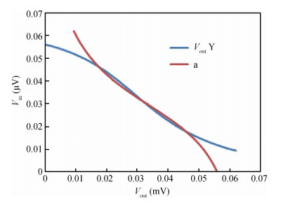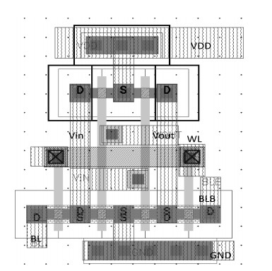
Fig. 1.
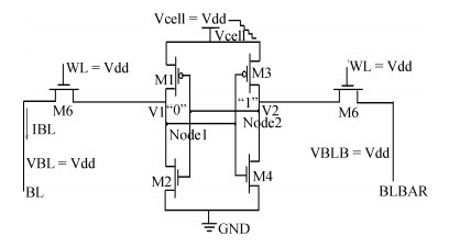
6T SRAM for hold (used for butterfly curve)
SEMICONDUCTOR INTEGRATED CIRCUITS
Ruchi1 and S.Dasgupta1,
Corresponding author: S.Dasgupta, Email:sudebfec@iitr.ac.in
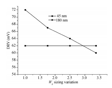
Abstract: The present paper analyzes the hold and read stability with temperature and aspect ratio variations. To reduce the power dissipation, one of the effective techniques is the supply voltage reduction. At this reduced supply voltage the data must be stable. So, the minimum voltage should be discovered which can also retain the data. This voltage is the data retention voltage (DRV). The DRV for 6T SRAM cell is estimated and analyzed in this paper. The sensitivity analysis is performed for the DRV variation with the variation in the temperature and aspect ratio of the pull up and pull down transistors. Cadence Virtuoso is used for DRV analysis using 45 nm GPDK technology files. After this, the read stability analysis of 6T SRAM cell in terms of SRRV (supply read retention voltage) and WRRV (wordline read retention voltage) is carried out. Read stability in terms of RSNM can be discovered by accessing the internal storage nodes. But in the case of dense SRAM arrays instead of using internal storage nodes, the stability can be discovered by using direct bit line measurements with the help of SRRV and WRRV. SRRV is used to find the minimum supply voltage for which data can be retained during a read operation. Similarly, WRRV is used to find the boosted value of wordline voltage, for which data can be retained during read operation. The SRRV and WRRV values are then analyzed for different Cell Ratios. The results of SRRV and WRRV are then compared with the reported data for the validation of the accuracy of the results.
Keywords: DRV, SRRV, WRRV, data retention, leakage reduction, low power SRAM, sensitivity analysis
| [1] |
Qin H F, Cao Y, Markovic D, et al. Standby supply voltage minimization for deep sub-micron SRAM. Microelectron J, 2005, 36:789 doi: 10.1016/j.mejo.2005.03.003
|
| [2] |
Sharifkhani M, Sachdev M. SRAM cell stability:a dynamic perspective. IEEE J Solid-State Circuits, 2009, 44(2):609 doi: 10.1109/JSSC.2008.2010818
|
| [3] |
Gupta V, Anis M. Statistical design of the 6T SRAM bit cell. IEEE Trans CAS-I, 2010, 57(1):93 doi: 10.1109/TCSI.2009.2016633
|
| [4] |
Oniciuc L, Andrei P. Sensitivity of static noise margins to random dopant variations in 6-T SRAM cells. Solid-State Electron, 2008, 52:1542 doi: 10.1016/j.sse.2008.06.029
|
| [5] |
Islam A, Hasan M. A technique to mitigate impact of process, voltage and temperature variations on design metrics of SRAM cell. Microelectron Reliab, 2012, 52:405 doi: 10.1016/j.microrel.2011.09.034
|
| [6] |
Chang I J, Kim J J, Park S P, et al. A 32 kB 10T sub-threshold SRAM array with bit-interleaving and differential read scheme in 90 nm CMOS. IEEE J Solid-State Circuits, 2009, 44(2):650 doi: 10.1109/JSSC.2008.2011972
|
| [7] |
Anh-Tuan D, Low J Y S, Low J Y L, et al. An 8T differential SRAM with improved noise margin for bit-interleaving in 65 nm CMOS. IEEE Trans CAS-I, 2011, 58(6):1252 doi: 10.1109/TCSI.2010.2103154
|
| [8] |
Yamauchi H. A discussion on SRAM circuit design trend in deeper nanometer-scale technologies. IEEE Trans VLSI Syst, 2010, 18(5):763 doi: 10.1109/TVLSI.2009.2016205
|
| [9] |
El Husseini J, Garros X, Cluzel J, et al. A complete characterization and modeling of the BTI-induced dynamic variability of SRAM arrays in 28-nm FD-SOI technology. IEEE Trans Electron Devices, 2014, 61(12):3991 doi: 10.1109/TED.2014.2361954
|
| [10] |
Singh J, Mohanty S P, Pradhan D K. Robust SRAM designs and analysis. Springer, 2013:31 doi: 10.1007%2F978-1-4614-0818-5
|
| [11] |
Pavlov A, Sachdev M. CMOS SRAM circuit design and parametric test in nano-scaled technologies. Springer, 2008 http://link.springer.com/content/pdf/bfm%3A978-1-4020-8363-1%2F1.pdf
|
| [12] |
Zheng G. Large scale variability characterization and robust design techniques for nanoscale SRAM. PhD Thesis, University of California, Berkeley, 2009 http://www.doc88.com/p-5406908454154.html
|
| [13] |
El Husseini J, Subirats A, Garros X. Accurate modeling of dynamic variability of SRAM cell in 28 nm FDSOI technology. IEEE Conference on Microelectronic Test Structures, Udine, Italy, 2014:41 https://www.researchgate.net/publication/259744552_Accurate_modeling_of_dynamic_variability_of_SRAM_cell_in_28_nm_FDSOI_technology
|
| [14] |
Bromio X A, Rajaram A. Energy efficient nano ram cell for the energy efficient operation. Int J Adv Inform Sci and Technol (IJAIST), 2014, 23(23):310
|
| [15] |
El Husseini J, Garros X, Subirats A, et al. Direct measurement of the dynamic variability of 0.120 μm 2 SRAM cells in 28 nm FDSOI technology. 2014 Symposium on VLSI Technology Digest of Technical Papers, 2014
|
| [16] |
Ruchi, Dasgupta S. Sensitivity analysis of DRV for various configurations of SRAM. 19th International Symposium on VLSI Design and Test (VDAT), 2015:1
|
| [17] |
Liu L, Yue S G, Lu S J. A four-interleaving HBD SRAM cell based on dual DICE for multiple node collection mitigation. J Semicond, 2015, 36(11):115007 doi: 10.1088/1674-4926/36/11/115007
|
| [18] |
Paul B C, Agarwal A, Roy K. Low-power techniques for scaled technologies. Integr VLSI J, 2006, 39:64 doi: 10.1016/j.vlsi.2005.12.001
|
| [19] |
Makosiej A, Thomas O, Amara A, et al. CMOS SRAM scaling limits under optimum stability constraints. ISCAS, 2013:1460
|
| [20] |
Guo Z, Carlson A, Pang L T, et al. Large scale SRAM variability characterization in 45 nm CMOS. IEEE J Solid-State Circuits, 2009, 44(11):3174 doi: 10.1109/JSSC.2009.2032698
|
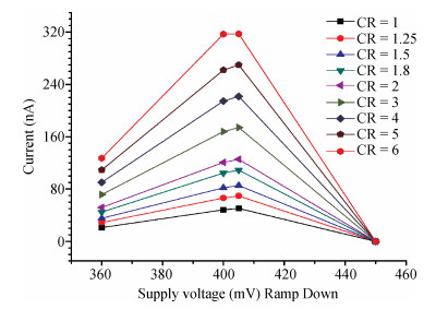
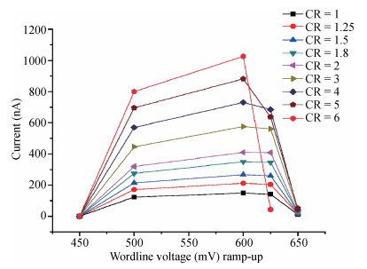
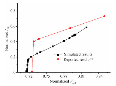
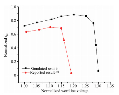
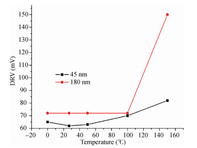
Table 1. DRV variation with temperature.

|
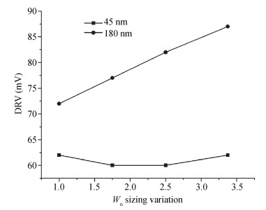
Table 2. DRV variation with Wn and Wp variation.

|
Table 3. The sizes of the transistors (Wn or Wp).

|
| [1] |
Qin H F, Cao Y, Markovic D, et al. Standby supply voltage minimization for deep sub-micron SRAM. Microelectron J, 2005, 36:789 doi: 10.1016/j.mejo.2005.03.003
|
| [2] |
Sharifkhani M, Sachdev M. SRAM cell stability:a dynamic perspective. IEEE J Solid-State Circuits, 2009, 44(2):609 doi: 10.1109/JSSC.2008.2010818
|
| [3] |
Gupta V, Anis M. Statistical design of the 6T SRAM bit cell. IEEE Trans CAS-I, 2010, 57(1):93 doi: 10.1109/TCSI.2009.2016633
|
| [4] |
Oniciuc L, Andrei P. Sensitivity of static noise margins to random dopant variations in 6-T SRAM cells. Solid-State Electron, 2008, 52:1542 doi: 10.1016/j.sse.2008.06.029
|
| [5] |
Islam A, Hasan M. A technique to mitigate impact of process, voltage and temperature variations on design metrics of SRAM cell. Microelectron Reliab, 2012, 52:405 doi: 10.1016/j.microrel.2011.09.034
|
| [6] |
Chang I J, Kim J J, Park S P, et al. A 32 kB 10T sub-threshold SRAM array with bit-interleaving and differential read scheme in 90 nm CMOS. IEEE J Solid-State Circuits, 2009, 44(2):650 doi: 10.1109/JSSC.2008.2011972
|
| [7] |
Anh-Tuan D, Low J Y S, Low J Y L, et al. An 8T differential SRAM with improved noise margin for bit-interleaving in 65 nm CMOS. IEEE Trans CAS-I, 2011, 58(6):1252 doi: 10.1109/TCSI.2010.2103154
|
| [8] |
Yamauchi H. A discussion on SRAM circuit design trend in deeper nanometer-scale technologies. IEEE Trans VLSI Syst, 2010, 18(5):763 doi: 10.1109/TVLSI.2009.2016205
|
| [9] |
El Husseini J, Garros X, Cluzel J, et al. A complete characterization and modeling of the BTI-induced dynamic variability of SRAM arrays in 28-nm FD-SOI technology. IEEE Trans Electron Devices, 2014, 61(12):3991 doi: 10.1109/TED.2014.2361954
|
| [10] |
Singh J, Mohanty S P, Pradhan D K. Robust SRAM designs and analysis. Springer, 2013:31 doi: 10.1007%2F978-1-4614-0818-5
|
| [11] |
Pavlov A, Sachdev M. CMOS SRAM circuit design and parametric test in nano-scaled technologies. Springer, 2008 http://link.springer.com/content/pdf/bfm%3A978-1-4020-8363-1%2F1.pdf
|
| [12] |
Zheng G. Large scale variability characterization and robust design techniques for nanoscale SRAM. PhD Thesis, University of California, Berkeley, 2009 http://www.doc88.com/p-5406908454154.html
|
| [13] |
El Husseini J, Subirats A, Garros X. Accurate modeling of dynamic variability of SRAM cell in 28 nm FDSOI technology. IEEE Conference on Microelectronic Test Structures, Udine, Italy, 2014:41 https://www.researchgate.net/publication/259744552_Accurate_modeling_of_dynamic_variability_of_SRAM_cell_in_28_nm_FDSOI_technology
|
| [14] |
Bromio X A, Rajaram A. Energy efficient nano ram cell for the energy efficient operation. Int J Adv Inform Sci and Technol (IJAIST), 2014, 23(23):310
|
| [15] |
El Husseini J, Garros X, Subirats A, et al. Direct measurement of the dynamic variability of 0.120 μm 2 SRAM cells in 28 nm FDSOI technology. 2014 Symposium on VLSI Technology Digest of Technical Papers, 2014
|
| [16] |
Ruchi, Dasgupta S. Sensitivity analysis of DRV for various configurations of SRAM. 19th International Symposium on VLSI Design and Test (VDAT), 2015:1
|
| [17] |
Liu L, Yue S G, Lu S J. A four-interleaving HBD SRAM cell based on dual DICE for multiple node collection mitigation. J Semicond, 2015, 36(11):115007 doi: 10.1088/1674-4926/36/11/115007
|
| [18] |
Paul B C, Agarwal A, Roy K. Low-power techniques for scaled technologies. Integr VLSI J, 2006, 39:64 doi: 10.1016/j.vlsi.2005.12.001
|
| [19] |
Makosiej A, Thomas O, Amara A, et al. CMOS SRAM scaling limits under optimum stability constraints. ISCAS, 2013:1460
|
| [20] |
Guo Z, Carlson A, Pang L T, et al. Large scale SRAM variability characterization in 45 nm CMOS. IEEE J Solid-State Circuits, 2009, 44(11):3174 doi: 10.1109/JSSC.2009.2032698
|


Article views: 6122 Times PDF downloads: 148 Times Cited by: 0 Times
Received: 07 March 2016 Revised: 02 September 2016 Online: Published: 01 February 2017
| Citation: |
Ruchi, S.Dasgupta. 6T SRAM cell analysis for DRV and read stability[J]. Journal of Semiconductors, 2017, 38(2): 025001. doi: 10.1088/1674-4926/38/2/025001
****
Ruchi, S. Dasgupta. 6T SRAM cell analysis for DRV and read stability[J]. J. Semicond., 2017, 38(2): 025001. doi: 10.1088/1674-4926/38/2/025001.

|
| [1] |
Qin H F, Cao Y, Markovic D, et al. Standby supply voltage minimization for deep sub-micron SRAM. Microelectron J, 2005, 36:789 doi: 10.1016/j.mejo.2005.03.003
|
| [2] |
Sharifkhani M, Sachdev M. SRAM cell stability:a dynamic perspective. IEEE J Solid-State Circuits, 2009, 44(2):609 doi: 10.1109/JSSC.2008.2010818
|
| [3] |
Gupta V, Anis M. Statistical design of the 6T SRAM bit cell. IEEE Trans CAS-I, 2010, 57(1):93 doi: 10.1109/TCSI.2009.2016633
|
| [4] |
Oniciuc L, Andrei P. Sensitivity of static noise margins to random dopant variations in 6-T SRAM cells. Solid-State Electron, 2008, 52:1542 doi: 10.1016/j.sse.2008.06.029
|
| [5] |
Islam A, Hasan M. A technique to mitigate impact of process, voltage and temperature variations on design metrics of SRAM cell. Microelectron Reliab, 2012, 52:405 doi: 10.1016/j.microrel.2011.09.034
|
| [6] |
Chang I J, Kim J J, Park S P, et al. A 32 kB 10T sub-threshold SRAM array with bit-interleaving and differential read scheme in 90 nm CMOS. IEEE J Solid-State Circuits, 2009, 44(2):650 doi: 10.1109/JSSC.2008.2011972
|
| [7] |
Anh-Tuan D, Low J Y S, Low J Y L, et al. An 8T differential SRAM with improved noise margin for bit-interleaving in 65 nm CMOS. IEEE Trans CAS-I, 2011, 58(6):1252 doi: 10.1109/TCSI.2010.2103154
|
| [8] |
Yamauchi H. A discussion on SRAM circuit design trend in deeper nanometer-scale technologies. IEEE Trans VLSI Syst, 2010, 18(5):763 doi: 10.1109/TVLSI.2009.2016205
|
| [9] |
El Husseini J, Garros X, Cluzel J, et al. A complete characterization and modeling of the BTI-induced dynamic variability of SRAM arrays in 28-nm FD-SOI technology. IEEE Trans Electron Devices, 2014, 61(12):3991 doi: 10.1109/TED.2014.2361954
|
| [10] |
Singh J, Mohanty S P, Pradhan D K. Robust SRAM designs and analysis. Springer, 2013:31 doi: 10.1007%2F978-1-4614-0818-5
|
| [11] |
Pavlov A, Sachdev M. CMOS SRAM circuit design and parametric test in nano-scaled technologies. Springer, 2008 http://link.springer.com/content/pdf/bfm%3A978-1-4020-8363-1%2F1.pdf
|
| [12] |
Zheng G. Large scale variability characterization and robust design techniques for nanoscale SRAM. PhD Thesis, University of California, Berkeley, 2009 http://www.doc88.com/p-5406908454154.html
|
| [13] |
El Husseini J, Subirats A, Garros X. Accurate modeling of dynamic variability of SRAM cell in 28 nm FDSOI technology. IEEE Conference on Microelectronic Test Structures, Udine, Italy, 2014:41 https://www.researchgate.net/publication/259744552_Accurate_modeling_of_dynamic_variability_of_SRAM_cell_in_28_nm_FDSOI_technology
|
| [14] |
Bromio X A, Rajaram A. Energy efficient nano ram cell for the energy efficient operation. Int J Adv Inform Sci and Technol (IJAIST), 2014, 23(23):310
|
| [15] |
El Husseini J, Garros X, Subirats A, et al. Direct measurement of the dynamic variability of 0.120 μm 2 SRAM cells in 28 nm FDSOI technology. 2014 Symposium on VLSI Technology Digest of Technical Papers, 2014
|
| [16] |
Ruchi, Dasgupta S. Sensitivity analysis of DRV for various configurations of SRAM. 19th International Symposium on VLSI Design and Test (VDAT), 2015:1
|
| [17] |
Liu L, Yue S G, Lu S J. A four-interleaving HBD SRAM cell based on dual DICE for multiple node collection mitigation. J Semicond, 2015, 36(11):115007 doi: 10.1088/1674-4926/36/11/115007
|
| [18] |
Paul B C, Agarwal A, Roy K. Low-power techniques for scaled technologies. Integr VLSI J, 2006, 39:64 doi: 10.1016/j.vlsi.2005.12.001
|
| [19] |
Makosiej A, Thomas O, Amara A, et al. CMOS SRAM scaling limits under optimum stability constraints. ISCAS, 2013:1460
|
| [20] |
Guo Z, Carlson A, Pang L T, et al. Large scale SRAM variability characterization in 45 nm CMOS. IEEE J Solid-State Circuits, 2009, 44(11):3174 doi: 10.1109/JSSC.2009.2032698
|

 WeChat ID
Journal of Semiconductors © 2017 All Rights Reserved 京ICP备05085259号-2

 DownLoad: