


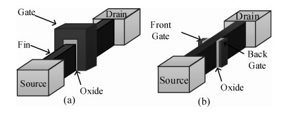
Fig. 1.
Three-dimensional structure of FinFET transistors. (a) 3T FinFET. (b) 4T FinFET.
SEMICONDUCTOR DEVICES
Tian Wang1, Xiaoxin Cui1, , Yewen Ni1, Kai Liao1, Nan Liao1, Dunshan Yu1 and Xiaole Cui2,
Corresponding author: Xiaoxin Cui, Email: cuixx@pku.edu.cn; Xiaole Cui, Email: cuixl@pkusz.edu.cn
Abstract: With shrinking transistor feature size, the fin-type field-effect transistor (FinFET) has become the most promising option in low-power circuit design due to its superior capability to suppress leakage. To support the VLSI digital system flow based on logic synthesis, we have designed an optimized high-performance low-power FinFET standard cell library based on employing the mixed FBB/RBB technique in the existing stacked structure of each cell. This paper presents the reliability evaluation of the optimized cells under process and operating environment variations based on Monte Carlo analysis. The variations are modelled with Gaussian distribution of the device parameters and 10000 sweeps are conducted in the simulation to obtain the statistical properties of the worst-case delay and input-dependent leakage for each cell. For comparison, a set of non-optimal cells that adopt the same topology without employing the mixed biasing technique is also generated. Experimental results show that the optimized cells achieve standard deviation reduction of 39.1% and 30.7% at most in worst-case delay and input-dependent leakage respectively while the normalized deviation shrinking in worst-case delay and input-dependent leakage can be up to 98.37% and 24.13%, respectively, which demonstrates that our optimized cells are less sensitive to variability and exhibit more reliability.
Keywords: reliability, FinFET, standard cell, low power, VLSI
| [1] |
Hu C, Bokor J, King T J, et al. FinFET-a self-aligned double-gate MOSFET scalable to 20 nm. IEEE Trans Electron Devices, 2000, 47(12): 2320 doi: 10.1109/16.887014
|
| [2] |
Xu M, Yin H X, Zhu H L, et al. Device parameter optimization for sub-20 nm node HK/MG-last bulk FinFETs. J Semicond, 2015, 36(4): 044007 doi: 10.1088/1674-4926/36/4/044007
|
| [3] |
Guo Y L, Wang G L, Zhao C, et al. Simulation and characterization of stress in FinFETs using novel LKMC and nanobeam diffraction method. J Semicond, 2015, 36(8): 086001 doi: 10.1088/1674-4926/36/8/086001
|
| [4] |
Johnson M C, Somasekhar D, Chiou L Y, et al. Leakage control with efficient use of transistor stacks in single threshold CMOS. Design Automation Conference, 1999: 1 doi: 10.1109/DAC.1999.107
|
| [5] |
Narendra S, Borkar S, De V, et al. Scaling of stack effect and its application for leakage reduction. International Symposium on Low Power Electronics and Design, 2001: 195 https://www.researchgate.net/publication/262408852_Scaling_of_stack_effect_and_its_application_for_leakage_reduction
|
| [6] |
Tschanz J W, Narendra S G, Ye Y, et al. Dynamic-sleep transistor and body bias for active leakage power control of microprocessors. IEEE J Solid-State Circuits, 2003, 38(11): 1838 doi: 10.1109/JSSC.2003.818291
|
| [7] |
Baccarin D, Esseni D, Alioto M. Low-standby current 4T FinFET buffers: analysis and evaluation below 45 nm. 2010 IEEE International Conference on Microelectronics (ICM), 2010: 296 http://www.academia.edu/15635185/Low-standby_current_4T_FinFET_buffers_Analysis_and_evaluation_below_45_nm
|
| [8] |
Baccarin D, Esseni D, Alioto M. A novel back-biasing low-leakage technique for FinFET forced stacks. IEEE Trans Very Large Scale Integr Syst, 2011, 19(5): 2079 https://www.researchgate.net/publication/221380166_A_novel_back-biasing_low-leakage_technique_for_FinFET_forced_stacks
|
| [9] |
Baccarin D, Esseni D, Alioto M. Mixed FBB/RBB: a novel low-leakage technique for FinFET forced stacks. IEEE Trans Very Large Scale Integr Syst, 2012, 20(8): 1467 doi: 10.1109/TVLSI.2011.2158614
|
| [10] |
Liao K, Cui X X, Liao N, et al. Ultra-low power dissipation of improved complementary pass-transistor adiabatic logic circuits based on FinFETs. Sci Chin Inform Sci, 2014, 57(4): 1 doi: 10.1007/s11432-013-5051-y
|
| [11] |
Liao N, Cui X X, Liao K, et al. Low power adiabatic logic based on FinFETs. Sci Chin Inform Sci, 2014, 57(2): 1 https://www.researchgate.net/profile/Kaisheng_Ma/publication/271917691_Low_power_adiabatic_logic_based_on_FinFETs/links/57bbf74508ae9fdf82ef2e1c.pdf?origin=publication_list
|
| [12] |
Ma K S, Cui X X, Liao K, et al. Key characterization factors of accurate power modeling for FinFET circuits. Sci Chin Inform Sci, 2015, 58(2): 1 https://www.researchgate.net/publication/270825342_Key_characterization_factors_of_accurate_power_modeling_for_FinFET_circuits
|
| [13] |
Liao K, Cui X X, Liao N, et al. Leakage power reduction of adiabatic circuits based on FinFET devices. IEICE Trans Electron, 2013, E96(8): 1068 http://adsabs.harvard.edu/abs/2013IEITE..96.1068L
|
| [14] |
Liao K, Cui X, Liao N, et al. Design of D flip-flops with low power-delay product based on FinFET. IEEE International Conference on Solid-State and Integrated Circuit Technology, 2015
|
| [15] |
Cakici T, Kim K, Roy K. FinFET based SRAM design for low standby power applications. International Symposium on Quality Electronic Design, 2007: 127
|
| [16] |
Ma K, Liu H, Xiao Y, et al. Independently-controlled-gate FinFET 6T SRAM cell design for leakage current reduction and enhanced read access speed. IEEE Computer Society Symposium on VLSI, 2014: 296
|
| [17] |
Rasouli S H, Koike H, Banerjee K. High-speed low-power FinFET based domino logic. Asia South Pacific Design Automation Conference, Asp-Dac 2009, Yokohama, Japan, 2009: 829
|
| [18] |
Wang T, Cui X X, Liao K, et al. Low power high performance FinFET standard cells based on mixed back biasing technology. IEICE Trans Electrons, 2016, 99(8): 974 https://www.researchgate.net/publication/305762552_Low_Power_High_Performance_FinFET_Standard_Cells_Based_on_Mixed_Back_Biasing_Technology
|
| [19] |
Predictive Technology Model (http://ptm.asu.edu/). Nanoscale Integration and Modeling (NIMO) Group, ASU
|
| [20] |
Cui X, Ma K, Liao K, et al. A dynamic-adjusting threshold-voltage scheme for FinFETs low power designs. 2013 IEEE International Symposium on Circuits and Systems (ISCAS, 2013: 129
|
| [21] |
Jin O. Power optimization for FinFET-based circuits using genetic algorithms. 2008 IEEE International SOC Conference, 2008: 211
|
| [22] |
Narendra S, De V, Borkar S, et al. Full-chip subthreshold leakage power prediction and reduction techniques for sub-0.18-μm CMOS. IEEE J Solid-State Circuits, 2004, 39(3): 501 doi: 10.1109/JSSC.2003.821776
|
| [23] |
Suresh D, Nagarajan K K, Srinivasan R. The impact of process variations on input impedance and mitigation using a circuit technique in FinFET-based LNA. J Semicond, 2015, 36(4): 045002 doi: 10.1088/1674-4926/36/4/045002
|
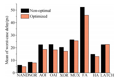

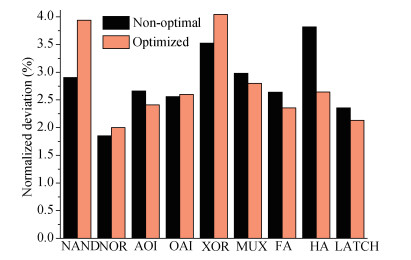
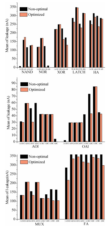
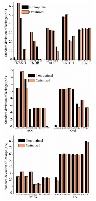
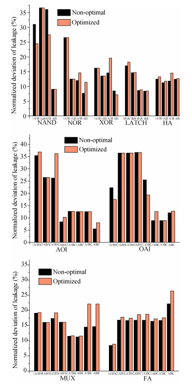
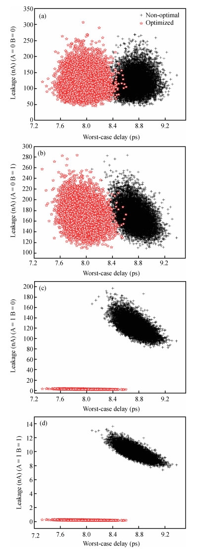
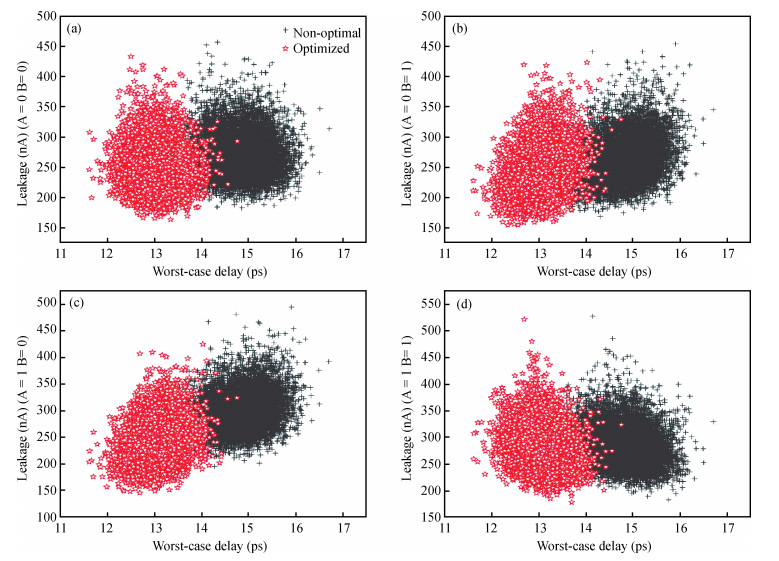
Table 1. Input-dependent back-gate bias voltages of NAND gate in the original and modified method.

|
Table 2. Parameters' mean value and deviations

|
| [1] |
Hu C, Bokor J, King T J, et al. FinFET-a self-aligned double-gate MOSFET scalable to 20 nm. IEEE Trans Electron Devices, 2000, 47(12): 2320 doi: 10.1109/16.887014
|
| [2] |
Xu M, Yin H X, Zhu H L, et al. Device parameter optimization for sub-20 nm node HK/MG-last bulk FinFETs. J Semicond, 2015, 36(4): 044007 doi: 10.1088/1674-4926/36/4/044007
|
| [3] |
Guo Y L, Wang G L, Zhao C, et al. Simulation and characterization of stress in FinFETs using novel LKMC and nanobeam diffraction method. J Semicond, 2015, 36(8): 086001 doi: 10.1088/1674-4926/36/8/086001
|
| [4] |
Johnson M C, Somasekhar D, Chiou L Y, et al. Leakage control with efficient use of transistor stacks in single threshold CMOS. Design Automation Conference, 1999: 1 doi: 10.1109/DAC.1999.107
|
| [5] |
Narendra S, Borkar S, De V, et al. Scaling of stack effect and its application for leakage reduction. International Symposium on Low Power Electronics and Design, 2001: 195 https://www.researchgate.net/publication/262408852_Scaling_of_stack_effect_and_its_application_for_leakage_reduction
|
| [6] |
Tschanz J W, Narendra S G, Ye Y, et al. Dynamic-sleep transistor and body bias for active leakage power control of microprocessors. IEEE J Solid-State Circuits, 2003, 38(11): 1838 doi: 10.1109/JSSC.2003.818291
|
| [7] |
Baccarin D, Esseni D, Alioto M. Low-standby current 4T FinFET buffers: analysis and evaluation below 45 nm. 2010 IEEE International Conference on Microelectronics (ICM), 2010: 296 http://www.academia.edu/15635185/Low-standby_current_4T_FinFET_buffers_Analysis_and_evaluation_below_45_nm
|
| [8] |
Baccarin D, Esseni D, Alioto M. A novel back-biasing low-leakage technique for FinFET forced stacks. IEEE Trans Very Large Scale Integr Syst, 2011, 19(5): 2079 https://www.researchgate.net/publication/221380166_A_novel_back-biasing_low-leakage_technique_for_FinFET_forced_stacks
|
| [9] |
Baccarin D, Esseni D, Alioto M. Mixed FBB/RBB: a novel low-leakage technique for FinFET forced stacks. IEEE Trans Very Large Scale Integr Syst, 2012, 20(8): 1467 doi: 10.1109/TVLSI.2011.2158614
|
| [10] |
Liao K, Cui X X, Liao N, et al. Ultra-low power dissipation of improved complementary pass-transistor adiabatic logic circuits based on FinFETs. Sci Chin Inform Sci, 2014, 57(4): 1 doi: 10.1007/s11432-013-5051-y
|
| [11] |
Liao N, Cui X X, Liao K, et al. Low power adiabatic logic based on FinFETs. Sci Chin Inform Sci, 2014, 57(2): 1 https://www.researchgate.net/profile/Kaisheng_Ma/publication/271917691_Low_power_adiabatic_logic_based_on_FinFETs/links/57bbf74508ae9fdf82ef2e1c.pdf?origin=publication_list
|
| [12] |
Ma K S, Cui X X, Liao K, et al. Key characterization factors of accurate power modeling for FinFET circuits. Sci Chin Inform Sci, 2015, 58(2): 1 https://www.researchgate.net/publication/270825342_Key_characterization_factors_of_accurate_power_modeling_for_FinFET_circuits
|
| [13] |
Liao K, Cui X X, Liao N, et al. Leakage power reduction of adiabatic circuits based on FinFET devices. IEICE Trans Electron, 2013, E96(8): 1068 http://adsabs.harvard.edu/abs/2013IEITE..96.1068L
|
| [14] |
Liao K, Cui X, Liao N, et al. Design of D flip-flops with low power-delay product based on FinFET. IEEE International Conference on Solid-State and Integrated Circuit Technology, 2015
|
| [15] |
Cakici T, Kim K, Roy K. FinFET based SRAM design for low standby power applications. International Symposium on Quality Electronic Design, 2007: 127
|
| [16] |
Ma K, Liu H, Xiao Y, et al. Independently-controlled-gate FinFET 6T SRAM cell design for leakage current reduction and enhanced read access speed. IEEE Computer Society Symposium on VLSI, 2014: 296
|
| [17] |
Rasouli S H, Koike H, Banerjee K. High-speed low-power FinFET based domino logic. Asia South Pacific Design Automation Conference, Asp-Dac 2009, Yokohama, Japan, 2009: 829
|
| [18] |
Wang T, Cui X X, Liao K, et al. Low power high performance FinFET standard cells based on mixed back biasing technology. IEICE Trans Electrons, 2016, 99(8): 974 https://www.researchgate.net/publication/305762552_Low_Power_High_Performance_FinFET_Standard_Cells_Based_on_Mixed_Back_Biasing_Technology
|
| [19] |
Predictive Technology Model (http://ptm.asu.edu/). Nanoscale Integration and Modeling (NIMO) Group, ASU
|
| [20] |
Cui X, Ma K, Liao K, et al. A dynamic-adjusting threshold-voltage scheme for FinFETs low power designs. 2013 IEEE International Symposium on Circuits and Systems (ISCAS, 2013: 129
|
| [21] |
Jin O. Power optimization for FinFET-based circuits using genetic algorithms. 2008 IEEE International SOC Conference, 2008: 211
|
| [22] |
Narendra S, De V, Borkar S, et al. Full-chip subthreshold leakage power prediction and reduction techniques for sub-0.18-μm CMOS. IEEE J Solid-State Circuits, 2004, 39(3): 501 doi: 10.1109/JSSC.2003.821776
|
| [23] |
Suresh D, Nagarajan K K, Srinivasan R. The impact of process variations on input impedance and mitigation using a circuit technique in FinFET-based LNA. J Semicond, 2015, 36(4): 045002 doi: 10.1088/1674-4926/36/4/045002
|


Article views: 4050 Times PDF downloads: 35 Times Cited by: 0 Times
Received: 10 August 2016 Revised: 03 October 2016 Online: Published: 01 April 2017
| Citation: |
Tian Wang, Xiaoxin Cui, Yewen Ni, Kai Liao, Nan Liao, Dunshan Yu, Xiaole Cui. Reliability evaluation of high-performance, low-power FinFET standard cells based on mixed RBB/FBB technique[J]. Journal of Semiconductors, 2017, 38(4): 044005. doi: 10.1088/1674-4926/38/4/044005
****
T Wang, X X Cui, Y W Ni, K Liao, N Liao, D S Yu, X L Cui. Reliability evaluation of high-performance, low-power FinFET standard cells based on mixed RBB/FBB technique[J]. J. Semicond., 2017, 38(4): 044005. doi: 10.1088/1674-4926/38/4/044005.

|
| [1] |
Hu C, Bokor J, King T J, et al. FinFET-a self-aligned double-gate MOSFET scalable to 20 nm. IEEE Trans Electron Devices, 2000, 47(12): 2320 doi: 10.1109/16.887014
|
| [2] |
Xu M, Yin H X, Zhu H L, et al. Device parameter optimization for sub-20 nm node HK/MG-last bulk FinFETs. J Semicond, 2015, 36(4): 044007 doi: 10.1088/1674-4926/36/4/044007
|
| [3] |
Guo Y L, Wang G L, Zhao C, et al. Simulation and characterization of stress in FinFETs using novel LKMC and nanobeam diffraction method. J Semicond, 2015, 36(8): 086001 doi: 10.1088/1674-4926/36/8/086001
|
| [4] |
Johnson M C, Somasekhar D, Chiou L Y, et al. Leakage control with efficient use of transistor stacks in single threshold CMOS. Design Automation Conference, 1999: 1 doi: 10.1109/DAC.1999.107
|
| [5] |
Narendra S, Borkar S, De V, et al. Scaling of stack effect and its application for leakage reduction. International Symposium on Low Power Electronics and Design, 2001: 195 https://www.researchgate.net/publication/262408852_Scaling_of_stack_effect_and_its_application_for_leakage_reduction
|
| [6] |
Tschanz J W, Narendra S G, Ye Y, et al. Dynamic-sleep transistor and body bias for active leakage power control of microprocessors. IEEE J Solid-State Circuits, 2003, 38(11): 1838 doi: 10.1109/JSSC.2003.818291
|
| [7] |
Baccarin D, Esseni D, Alioto M. Low-standby current 4T FinFET buffers: analysis and evaluation below 45 nm. 2010 IEEE International Conference on Microelectronics (ICM), 2010: 296 http://www.academia.edu/15635185/Low-standby_current_4T_FinFET_buffers_Analysis_and_evaluation_below_45_nm
|
| [8] |
Baccarin D, Esseni D, Alioto M. A novel back-biasing low-leakage technique for FinFET forced stacks. IEEE Trans Very Large Scale Integr Syst, 2011, 19(5): 2079 https://www.researchgate.net/publication/221380166_A_novel_back-biasing_low-leakage_technique_for_FinFET_forced_stacks
|
| [9] |
Baccarin D, Esseni D, Alioto M. Mixed FBB/RBB: a novel low-leakage technique for FinFET forced stacks. IEEE Trans Very Large Scale Integr Syst, 2012, 20(8): 1467 doi: 10.1109/TVLSI.2011.2158614
|
| [10] |
Liao K, Cui X X, Liao N, et al. Ultra-low power dissipation of improved complementary pass-transistor adiabatic logic circuits based on FinFETs. Sci Chin Inform Sci, 2014, 57(4): 1 doi: 10.1007/s11432-013-5051-y
|
| [11] |
Liao N, Cui X X, Liao K, et al. Low power adiabatic logic based on FinFETs. Sci Chin Inform Sci, 2014, 57(2): 1 https://www.researchgate.net/profile/Kaisheng_Ma/publication/271917691_Low_power_adiabatic_logic_based_on_FinFETs/links/57bbf74508ae9fdf82ef2e1c.pdf?origin=publication_list
|
| [12] |
Ma K S, Cui X X, Liao K, et al. Key characterization factors of accurate power modeling for FinFET circuits. Sci Chin Inform Sci, 2015, 58(2): 1 https://www.researchgate.net/publication/270825342_Key_characterization_factors_of_accurate_power_modeling_for_FinFET_circuits
|
| [13] |
Liao K, Cui X X, Liao N, et al. Leakage power reduction of adiabatic circuits based on FinFET devices. IEICE Trans Electron, 2013, E96(8): 1068 http://adsabs.harvard.edu/abs/2013IEITE..96.1068L
|
| [14] |
Liao K, Cui X, Liao N, et al. Design of D flip-flops with low power-delay product based on FinFET. IEEE International Conference on Solid-State and Integrated Circuit Technology, 2015
|
| [15] |
Cakici T, Kim K, Roy K. FinFET based SRAM design for low standby power applications. International Symposium on Quality Electronic Design, 2007: 127
|
| [16] |
Ma K, Liu H, Xiao Y, et al. Independently-controlled-gate FinFET 6T SRAM cell design for leakage current reduction and enhanced read access speed. IEEE Computer Society Symposium on VLSI, 2014: 296
|
| [17] |
Rasouli S H, Koike H, Banerjee K. High-speed low-power FinFET based domino logic. Asia South Pacific Design Automation Conference, Asp-Dac 2009, Yokohama, Japan, 2009: 829
|
| [18] |
Wang T, Cui X X, Liao K, et al. Low power high performance FinFET standard cells based on mixed back biasing technology. IEICE Trans Electrons, 2016, 99(8): 974 https://www.researchgate.net/publication/305762552_Low_Power_High_Performance_FinFET_Standard_Cells_Based_on_Mixed_Back_Biasing_Technology
|
| [19] |
Predictive Technology Model (http://ptm.asu.edu/). Nanoscale Integration and Modeling (NIMO) Group, ASU
|
| [20] |
Cui X, Ma K, Liao K, et al. A dynamic-adjusting threshold-voltage scheme for FinFETs low power designs. 2013 IEEE International Symposium on Circuits and Systems (ISCAS, 2013: 129
|
| [21] |
Jin O. Power optimization for FinFET-based circuits using genetic algorithms. 2008 IEEE International SOC Conference, 2008: 211
|
| [22] |
Narendra S, De V, Borkar S, et al. Full-chip subthreshold leakage power prediction and reduction techniques for sub-0.18-μm CMOS. IEEE J Solid-State Circuits, 2004, 39(3): 501 doi: 10.1109/JSSC.2003.821776
|
| [23] |
Suresh D, Nagarajan K K, Srinivasan R. The impact of process variations on input impedance and mitigation using a circuit technique in FinFET-based LNA. J Semicond, 2015, 36(4): 045002 doi: 10.1088/1674-4926/36/4/045002
|

 WeChat ID
Journal of Semiconductors © 2017 All Rights Reserved 京ICP备05085259号-2

 DownLoad:

