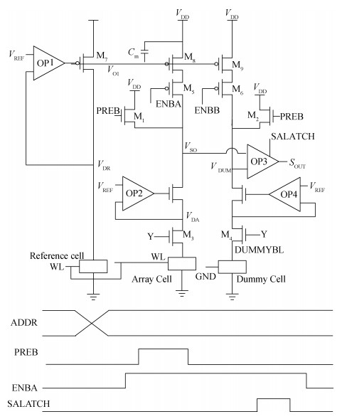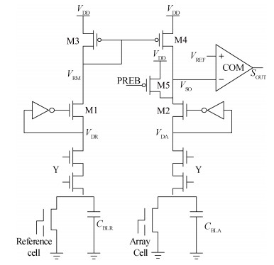
Fig. 1.
Conventional sense amplifier.
SEMICONDUCTOR INTEGRATED CIRCUITS
Corresponding author: Jiarong Guo, Email: jrguo@shu.edu.cn
Abstract: A low-voltage sense amplifier with reference current generator utilizing two-stage operational amplifier clamp structure for flash memory is presented in this paper, capable of operating with minimum supply voltage at 1 V. A new reference current generation circuit composed of a reference cell and a two-stage operational amplifier clamping the drain pole of the reference cell is used to generate the reference current, which avoids the threshold limitation caused by current mirror transistor in the traditional sense amplifier. A novel reference voltage generation circuit using dummy bit-line structure without pull-down current is also adopted, which not only improves the sense window enhancing read precision but also saves power consumption. The sense amplifier was implemented in a flash realized in 90 nm flash technology. Experimental results show the access time is 14.7 ns with power supply of 1.2 V and slow corner at 125 ℃.
Keywords: flash memory, sense amplifier, low voltage, two-stage operational amplifier, current sensing
| [1] |
Jefremow M, Kern T, Backhausen U, et al. Bitline-capacitance-cancelation sensing scheme with 11 ns read latency and maximum read throughput of 2. 9 GB/s in 65 nm embedded flash for automotive. Proc IEEE ISSCC, 2012: 428
|
| [2] |
Gao X M, Yuan W, Yan D G, et al. An innovative sensing architecture for multilevel flash memory. Solid-State and Integrated Circuit Technology (ICSICT), 2012: 1
|
| [3] |
Guo J R, Ran F. A new low-voltage and high-speed sense amplifier for flash memory. J Semicond, 2011, 32(12): 125003 doi: 10.1088/1674-4926/32/12/125003
|
| [4] |
Hsieh J W, Chang Y H, Chu Y S, et al. Implementation strategy for downloaded flash-memory storage devices. Trans Embedded Comput Sys, 2013, 12(1): 103 http://users.ece.cmu.edu/~omutlu/pub/persistent-memory-management_weed13.pdf
|
| [5] |
Li Z, Wang Z G, Li Z Q, et al. IC design of low power, wide tuning range VCO in 90 nm CMOS technology. J Semicond, 2014, 35(12): 125013 doi: 10.1088/1674-4926/35/12/125013
|
| [6] |
Wang Y, Xue C Y, Li F L, et al. A low power 11-bit 100 MS/s SAR ADC IP. J Semicond, 2015, 36(2): 025003 doi: 10.1088/1674-4926/36/2/025003
|
| [7] |
Duan J H, Deng D Y, Xu W L, et al. An extremely low power voltage reference with high PSRR for power-aware ASIC. J Semicond, 2015, 36(9): 095006 doi: 10.1088/1674-4926/36/9/095006
|
| [8] |
Tanzawa T, Tanaka Y, Takeuchi K, et al. Circuit techniques for a 1.8 V only NAND flash memory. Solid-State Circuits, 2002, 37(1): 84 doi: 10.1109/4.974549
|
| [9] |
Micheloni R, Crippa L, Sangalli M, et al. The flash memory read path: building blocks and critical aspects. Proc IEEE, 2003, 91(4): 537 doi: 10.1109/JPROC.2003.811704
|
| [10] |
Seo M K, Sim S H, Oh M H, et al A 130-nm 0.9 V 66-MHz 8 Mb (256 K×32) local SONOS embedded flash EEPROM. Solid-State Circuits, 2005, 40(4): 877 doi: 10.1109/JSSC.2005.845564
|
| [11] |
Liu J, Wang X Q, Wang W, et al. A low-voltage sense amplifier for high-performance embedded flash memory. J Semicond, 2010, 31(10): 1 https://www.researchgate.net/publication/229028730_A_low-voltage_sense_amplifier_for_high-performance_embedded_flash_memory
|
| [12] |
Tanzawa T, Takano Y, Taura T, et al. A 1.2 V sense amplifier for high-performance embeddable NOR flash memories. Proc ISCAS, 2005, 2: 1266
|
| [13] |
Antonino C, Gianbattista L G, Gaetano P, et al. A high-performance very low-voltage current sense amplifier for nonvolatile memories. Solid-State Circuits, 2005, 40(2): 507 doi: 10.1109/JSSC.2004.840985
|
| [14] |
Zhang H, Lu L. A low voltage sense amplifier for embedded flash memories. IEEE Trans Circuits Syst â…¡, 2015, 62(3): 236 http://www.scientific.net/keyword/Embedded_Flash_Memories
|
| [15] |
Guo J R, Ran F, Xu, M H. A low-voltage sense amplifier based on resistor mirror. Acta Electron Sin, 2014, 42(5): 1030 https://www.researchgate.net/publication/290274169_A_low-voltage_sense_amplifier_based_on_resistor_mirror
|
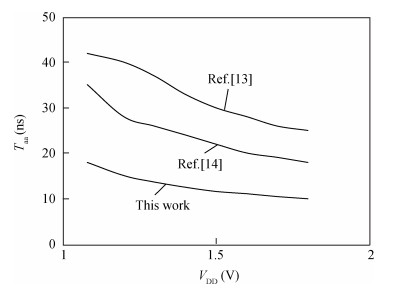
Table 1. The summary of reference current generating circuits.

|
| [1] |
Jefremow M, Kern T, Backhausen U, et al. Bitline-capacitance-cancelation sensing scheme with 11 ns read latency and maximum read throughput of 2. 9 GB/s in 65 nm embedded flash for automotive. Proc IEEE ISSCC, 2012: 428
|
| [2] |
Gao X M, Yuan W, Yan D G, et al. An innovative sensing architecture for multilevel flash memory. Solid-State and Integrated Circuit Technology (ICSICT), 2012: 1
|
| [3] |
Guo J R, Ran F. A new low-voltage and high-speed sense amplifier for flash memory. J Semicond, 2011, 32(12): 125003 doi: 10.1088/1674-4926/32/12/125003
|
| [4] |
Hsieh J W, Chang Y H, Chu Y S, et al. Implementation strategy for downloaded flash-memory storage devices. Trans Embedded Comput Sys, 2013, 12(1): 103 http://users.ece.cmu.edu/~omutlu/pub/persistent-memory-management_weed13.pdf
|
| [5] |
Li Z, Wang Z G, Li Z Q, et al. IC design of low power, wide tuning range VCO in 90 nm CMOS technology. J Semicond, 2014, 35(12): 125013 doi: 10.1088/1674-4926/35/12/125013
|
| [6] |
Wang Y, Xue C Y, Li F L, et al. A low power 11-bit 100 MS/s SAR ADC IP. J Semicond, 2015, 36(2): 025003 doi: 10.1088/1674-4926/36/2/025003
|
| [7] |
Duan J H, Deng D Y, Xu W L, et al. An extremely low power voltage reference with high PSRR for power-aware ASIC. J Semicond, 2015, 36(9): 095006 doi: 10.1088/1674-4926/36/9/095006
|
| [8] |
Tanzawa T, Tanaka Y, Takeuchi K, et al. Circuit techniques for a 1.8 V only NAND flash memory. Solid-State Circuits, 2002, 37(1): 84 doi: 10.1109/4.974549
|
| [9] |
Micheloni R, Crippa L, Sangalli M, et al. The flash memory read path: building blocks and critical aspects. Proc IEEE, 2003, 91(4): 537 doi: 10.1109/JPROC.2003.811704
|
| [10] |
Seo M K, Sim S H, Oh M H, et al A 130-nm 0.9 V 66-MHz 8 Mb (256 K×32) local SONOS embedded flash EEPROM. Solid-State Circuits, 2005, 40(4): 877 doi: 10.1109/JSSC.2005.845564
|
| [11] |
Liu J, Wang X Q, Wang W, et al. A low-voltage sense amplifier for high-performance embedded flash memory. J Semicond, 2010, 31(10): 1 https://www.researchgate.net/publication/229028730_A_low-voltage_sense_amplifier_for_high-performance_embedded_flash_memory
|
| [12] |
Tanzawa T, Takano Y, Taura T, et al. A 1.2 V sense amplifier for high-performance embeddable NOR flash memories. Proc ISCAS, 2005, 2: 1266
|
| [13] |
Antonino C, Gianbattista L G, Gaetano P, et al. A high-performance very low-voltage current sense amplifier for nonvolatile memories. Solid-State Circuits, 2005, 40(2): 507 doi: 10.1109/JSSC.2004.840985
|
| [14] |
Zhang H, Lu L. A low voltage sense amplifier for embedded flash memories. IEEE Trans Circuits Syst â…¡, 2015, 62(3): 236 http://www.scientific.net/keyword/Embedded_Flash_Memories
|
| [15] |
Guo J R, Ran F, Xu, M H. A low-voltage sense amplifier based on resistor mirror. Acta Electron Sin, 2014, 42(5): 1030 https://www.researchgate.net/publication/290274169_A_low-voltage_sense_amplifier_based_on_resistor_mirror
|


Article views: 4187 Times PDF downloads: 57 Times Cited by: 0 Times
Received: 29 March 2016 Revised: 27 September 2016 Online: Published: 01 April 2017
| Citation: |
Jiarong Guo. A low-voltage sense amplifier with two-stage operational amplifier clamping for flash memory[J]. Journal of Semiconductors, 2017, 38(4): 045001. doi: 10.1088/1674-4926/38/4/045001
****
J R Guo. A low-voltage sense amplifier with two-stage operational amplifier clamping for flash memory[J]. J. Semicond., 2017, 38(4): 045001. doi: 10.1088/1674-4926/38/4/045001.

|
| [1] |
Jefremow M, Kern T, Backhausen U, et al. Bitline-capacitance-cancelation sensing scheme with 11 ns read latency and maximum read throughput of 2. 9 GB/s in 65 nm embedded flash for automotive. Proc IEEE ISSCC, 2012: 428
|
| [2] |
Gao X M, Yuan W, Yan D G, et al. An innovative sensing architecture for multilevel flash memory. Solid-State and Integrated Circuit Technology (ICSICT), 2012: 1
|
| [3] |
Guo J R, Ran F. A new low-voltage and high-speed sense amplifier for flash memory. J Semicond, 2011, 32(12): 125003 doi: 10.1088/1674-4926/32/12/125003
|
| [4] |
Hsieh J W, Chang Y H, Chu Y S, et al. Implementation strategy for downloaded flash-memory storage devices. Trans Embedded Comput Sys, 2013, 12(1): 103 http://users.ece.cmu.edu/~omutlu/pub/persistent-memory-management_weed13.pdf
|
| [5] |
Li Z, Wang Z G, Li Z Q, et al. IC design of low power, wide tuning range VCO in 90 nm CMOS technology. J Semicond, 2014, 35(12): 125013 doi: 10.1088/1674-4926/35/12/125013
|
| [6] |
Wang Y, Xue C Y, Li F L, et al. A low power 11-bit 100 MS/s SAR ADC IP. J Semicond, 2015, 36(2): 025003 doi: 10.1088/1674-4926/36/2/025003
|
| [7] |
Duan J H, Deng D Y, Xu W L, et al. An extremely low power voltage reference with high PSRR for power-aware ASIC. J Semicond, 2015, 36(9): 095006 doi: 10.1088/1674-4926/36/9/095006
|
| [8] |
Tanzawa T, Tanaka Y, Takeuchi K, et al. Circuit techniques for a 1.8 V only NAND flash memory. Solid-State Circuits, 2002, 37(1): 84 doi: 10.1109/4.974549
|
| [9] |
Micheloni R, Crippa L, Sangalli M, et al. The flash memory read path: building blocks and critical aspects. Proc IEEE, 2003, 91(4): 537 doi: 10.1109/JPROC.2003.811704
|
| [10] |
Seo M K, Sim S H, Oh M H, et al A 130-nm 0.9 V 66-MHz 8 Mb (256 K×32) local SONOS embedded flash EEPROM. Solid-State Circuits, 2005, 40(4): 877 doi: 10.1109/JSSC.2005.845564
|
| [11] |
Liu J, Wang X Q, Wang W, et al. A low-voltage sense amplifier for high-performance embedded flash memory. J Semicond, 2010, 31(10): 1 https://www.researchgate.net/publication/229028730_A_low-voltage_sense_amplifier_for_high-performance_embedded_flash_memory
|
| [12] |
Tanzawa T, Takano Y, Taura T, et al. A 1.2 V sense amplifier for high-performance embeddable NOR flash memories. Proc ISCAS, 2005, 2: 1266
|
| [13] |
Antonino C, Gianbattista L G, Gaetano P, et al. A high-performance very low-voltage current sense amplifier for nonvolatile memories. Solid-State Circuits, 2005, 40(2): 507 doi: 10.1109/JSSC.2004.840985
|
| [14] |
Zhang H, Lu L. A low voltage sense amplifier for embedded flash memories. IEEE Trans Circuits Syst â…¡, 2015, 62(3): 236 http://www.scientific.net/keyword/Embedded_Flash_Memories
|
| [15] |
Guo J R, Ran F, Xu, M H. A low-voltage sense amplifier based on resistor mirror. Acta Electron Sin, 2014, 42(5): 1030 https://www.researchgate.net/publication/290274169_A_low-voltage_sense_amplifier_based_on_resistor_mirror
|

 WeChat ID
Journal of Semiconductors © 2017 All Rights Reserved 京ICP备05085259号-2

 DownLoad: