Processing math: 100%
J. Semicond. > 2017, Volume 38 > Issue 5 > 053002

SEMICONDUCTOR MATERIALS

Electrodeposition and characterization of ZnO thin films using sodium thiosulfate as an additive for photovoltaic solar cells

Hassiba Rahal1, 2, Rafiaa Kihal1, 3, Abed Mohamed Affoune1, , Mokhtar Ghers4 and Faycal Djazi5

+ Author Affiliations

 Corresponding author: Abed Mohamed Affoune Email: affoune2@yahoo.fr

DOI: 10.1088/1674-4926/38/5/053002

PDF

Abstract: Zinc oxide thin films have been grown by electrodeposition technique onto Cu and ITO-coated glass substrates from an aqueous zinc nitrate solution with addition of sodium thiosulfate at 90℃.The effects of sodium thiosulfate on the electrochemical deposition of ZnO were investigated by cyclic voltammetry and chronoamperometry techniques.Deposited films were obtained at-0:60 V vs.SCE and characterized by XRD, SEM, FTIR, optical, photoelectrochemical and electrical measurements.Thickness of the deposited film was measured to be 357 nm.X-ray diffraction results indicated that the synthesized ZnO has a pure hexagonal wurtzite structure with a marked preferential orientation along (002) plane.FTIR results confirmed the presence of ZnO films at peak 558 cm-1.SEM images showed uniform, compact morphology without any cracks and films composed of large flower-like ZnO agglomerates with star-shape.Optical properties of ZnO reveal a high optical transmission (>80%) and high absorption coefficient (α>105 cm-1) in visible region.The optical energy band gap was found to be 3.28 eV.Photoelectrochemical measurements indicated that the ZnO films had n-type semiconductor conduction.Electrical properties of ZnO films showed a low electrical resistivity of 6.54 Ω·cm, carrier concentration of-1.3×1017cm-3 and mobility of 7.35 cm2V-1s-1.

Key words: electrodepositionzinc oxidethin filmssemiconductorcyclic voltammetryHall effect measurements

The total demand of energy in the world increases with the demographic growth and the development of technology. Among all renewable energy sources, solar energy is extremely useful and promising as an abundant and clean energy source[1]. Photovoltaic conversion is one of the most advanced technologies, which consists in directly transforming solar energy into electric energy using a semiconductor and it has attracted attention for many decades. The high production cost of solar energy materials constitutes a serious drawback for the commercialization of photovoltaic cells. Furthermore, toxic substances are involved in the production and processing of most semiconductors, causing environmental problems. Thus, research efforts have been made, especially in the last decade, in order to develop materials which were able to guarantee optimal characteristics in terms of environmental compatibility, abundance and photoactivity[2]. Among the various metal oxide materials for photovoltaic applications, a promising material is zinc oxide (ZnO), one of the oldest known semiconductors. ZnO is an important binary Ⅱ-Ⅵ semiconductor compound because of its interesting properties such as resistivity control over the range 103-105Ωcm, transparency in the visible range, high electrochemical stability, direct band gap (3.3 eV) with large exciton binding energy of 60 meV at room temperature, absence of toxicity and good abundance in nature and high absorption coefficient suitable for solar cell applications. ZnO crystallizes preferentially in the hexagonal wurtzite structure and presents typically n-type electrical conductivity due to residual donors[3]. Thus it is promising in various applications, including laser diode[4], electronic and optoelectronic[5], phosphors[6], gas sensors[7]. They also can be used as transparent electrodes in dye-sensitized solar cells[8].

Various synthesis methods are usually used to prepare ZnO thin films, such as pulsed laser deposition[9], chemical vapor deposition[4], thermal oxidation[6], sol gel[10], photochemical deposition[11] and electrodeposition[12-15]. Besides these methods, electrodeposition provides several advantages over the other methods because of its simplicity, low equipment cost, the possibility of preparing large area thin films and the control of the film thickness[16]. ZnO thin films are usually electrodeposited from zinc precursor solution, such as zinc nitrate[17-20], zinc sulfate[21], zinc chloride[21-24]and zinc acetate[25, 26].

The growth mechanism in the electrochemical deposition of ZnO thin films is the reduction of an oxygen precursor at the interface of the electrode in the presence of zinc ions. Three main oxygen precursors have been described up to now: nitrate ions[12, 17, 18, 27, 28], dissolved molecular oxygen[25], and hydrogen peroxide[22, 29, 30]. Among them, the nitrate ion-based oxygen precursor has attracted considerable interest. Compared with other zinc precursors, the zinc nitrate precursor can act as both the zinc and oxygen precursor, which will simplify the electrolyte composition, and widen the adjustable range of oxygen concentration[31]. In order to improve the quality of the deposited films such as uniformity, adhesion and crystallinity, it is necessary to add a complexing agent into the electrolytic bath. Many researchers use various complexing agents such as polyvinylpyrolidone[19], lactic acid[20], tartaric acid[24], ethylene diamine tetra acetic acid[23, 26], citric acid[26] and sodium thiosulfate[11, 21, 32]. Furthermore, sodium thiosulfate shows a promising complexing agent of the deposited ZnO thin films because of its non-toxicity and low-cost compared to other complexing agents[19, 20, 23, 24, 26]. No work has been published concerning the electrodeposition of ZnO using sodium thiosulfate with zinc nitrate as precursor.

The aim of this work is devoted to the preparation of ZnO thin films onto Cu and ITO-coated glass substrates by electrodeposition technique in a solution of zinc nitrate with sodium thiosulfate. Cyclic voltammetry and chronoamperometry were utilized to study the electrochemical behavior of electrolyte bath containing zinc nitrate. The effect of sodium thiosulfate on the electrochemical deposition, structural and morphological of ZnO thin films was investigated. Deposited films were characterized by X-ray diffraction (XRD), Fourier transform infrared spectroscopy (FTIR), scanning electron microscopy (SEM), optical, photoelectrochemical (PEC) and electrical measurements.

All chemical reagents used in the present work were of analytical grade. Zinc nitrate hexahydrate (Zn (NO3)26H2O, 98%, Sigma Aldrich) was used as zinc and oxygen sources. However, sodium thiosulfate pentahydrate (Na2S2O35H2O, 99.5%, Sigma Aldrich) was added as complexing agent. All the aqueous solution was prepared using distilled water.

Electrodeposition of ZnO thin films was carried out using a three electrode electrochemical cell with a platinum (Pt) wire as a counter electrode, and copper (Cu) plates or indium tin oxide (ITO)-coated glass (8-10 Ω/square, Sigma Aldrich) substrates were used as working electrode. A saturated calomel electrode (SCE) was used in all experiments as a reference electrode. Before the deposition, the substrates were ultrasonically rinsed in 0.1 M HCl, distilled water, and acetone and then rinsed in distilled water[31, 24]. Zinc oxide thin films were electrodeposited in an aqueous solution of 0.1 M Zn (NO3)26H2O and 1.2 mM Na2S2O35H2O at 90 ℃. The pH of the solution was adjusted to 5.74 by NaOH additions. Sodium thiosulfate is used to stabilize Zn2+ ions in the solution[11, 21].

Cyclic voltammetry and chronoamperometry studies were carried out using Princeton Applied Research Model 273 A Potentiostat/Galvanostat, coupled to a personal computer with Power Suite software for data acquisition and potential control. Thin films of zinc oxide were electrodeposited at 0.60 V for 30 min. Following the deposition, the deposited ZnO films were dried in air at 100 ℃.

The crystalline phase of ZnO thin films was investigated by X-ray diffraction using a Bruker Discover D8 Diffractometer with CuKα radiation (λ=1.5406 Å). FTIR spectra were recorded on a Shimadzu FTIR-8000 series spectrophotometer in the wavelength range of 400-4000 cm1. Scanning electron microscopy imaging was performed using a VEGA3 TESCAN scanning electron microscope operating at 20 kV accelerating voltage. Optical transmittance of thin films was measured by a Perkin Elmer Lambda 950 UV-vis-NIR spectrometer in the wavelength range 200-1100 nm. Photoelectrochemical measurements were carried out by cyclic voltammetry technique in a three electrode electrochemical cell using deposited ZnO films as a working electrode, platinum wire as a counter electrode and a saturated calomel electrode (SCE) as a reference electrode from an aqueous solution containing 0.1 M sodium sulfate (Na2SO4). A tungsten halogen lamp (100 W) was used to illuminate an active area of 1.5 cm2 of ZnO electrode. Electrical properties of deposited ZnO films were determined by a HMS 3000 Hall measurement system at room temperature. Ag-paste was used at the corners of the films to make four good contacts with the probes. Thickness of the films was measured using Dektak stylus profilometer.

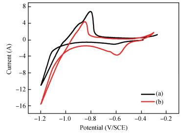
Fig. 1 shows the cyclic voltammograms of the solution containing 0.1 M zinc nitrate without (Fig. 1(a)) and with 1.2 mM sodium thiosulfate (Fig. 1(b)) at the same pH = 5.74 and T=90 ℃. The potential sweep was ranged from 0.2 to 1.2 V with a scan rate of 50 mV/s. From Fig. 1(a), the cathodic peak is observed around 0.61 V corresponding to the reduction of nitrate to nitrite ions with water molecules converted to hydroxide ions. These hydroxide ions combined with Zn2+ ions leading to the formation of Zn (OH)2, which dehydrated and converted to ZnO by the following mechanism[12]:

Figure  1.  Color online) Cyclic voltammograms of the solution containing 0.1 M Zn (NO3)26H2O at pH = 5.74 and T=90 ℃, (a) without and (b) with 1.2 mM sodium thiosulfate. The potential scanning rate was 50 mV/s.

Zn(NO3)2Zn2++2NO3,

(1)

NO3+H2O+2eNO2+2OH,

(2)

Zn2++2OHZn(OH)2ZnO+H2O.

(3)

From 1.1 V, an abrupt increase of cathodic current takes place, which can be mainly ascribed to the deposition of zinc with release of hydrogen [Eqs. (4) and (5)].

Zn2++2eZn, 

(4)

2H++2eH2.

(5)

During reverse anodic scan, an oxidation peak is observed at 0.8 V, which can be attributed to the anodic dissolution of zinc metal[27, 29, 33]. From Fig. 1(b), we can observe that in the presence of sodium thiosulfate, the cathodic peak current of the formation of ZnO is much higher which indicates an increase in the deposition rate of ZnO thin films, whereas the oxidation peak of zinc metal is decreased compared to that without sodium thiosulfate (Table 1). This difference can be attributed to a complexing effect of the Zn2+ ions by the sodium thiosulfate, leading to acceleration of the electrochemical reaction kinetics for the formation of ZnO thin films. This phenomenon was observed in Refs. [21, 24, 34]. The ratio between cathodic peak current with and without sodium thiosulfate is about 3.18. This value is higher than that of other complexing agents[20, 24].

Table  1.  Electrochemical parameters obtained from cyclic voltammograms.
DownLoad: CSV  | Show Table

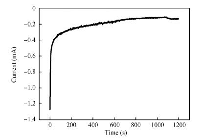
Fig. 2 shows the chronoamperometry curve for the deposition of ZnO thin films onto Cu substrate with sodium thiosulfate at T=90 ℃ and E=0.6 V. The current starts with high value, which is assigned to a rapid nucleation growth. The decrease of cathodic current as function of time is due to a depletion of the metal-ion concentrations close to the electrode surface. The current stabilized at even longer time (1200 s). This confirms that the limited value of the stationary current is related to the formation of zinc oxide on the surface. A similar behavior was observed for different zinc salt solutions with other complexing agents[13, 19, 26].

Figure  2.  Chronoamperometry curve for the deposition of ZnO thin films.

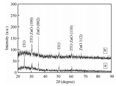
The thickness of the deposited films was measured to be 357 nm. Fig. 3 shows the XRD patterns of ZnO thin films deposited onto ITO-coated glass substrates without (Fig. 3(a)) and with sodium thiosulfate (Fig. 3(b)). From this figure, X-ray diffraction patterns indicate that the obtained ZnO thin films have a hexagonal wurtzite-type structure with preferable (002) growth direction and all the peaks of ZnO thin films correspond to the peaks of standard ZnO (Zincite phase JCPDS 36-1451). For the films prepared from the nitrate zinc solution containing sodium thiosulfate, the intensity of the (002) diffraction peak of ZnO is significantly higher than that of the films without sodium thiosulfate. It is also interesting to note that the sodium thiosulfate improved the good crystallinity of deposited ZnO thin films. The values calculated for lattice constant parameters of the ZnO films (a=b=3.2909 Å, c=5.1926 Å) were slightly different than those of standard ZnO (JCPDS 36-1451, a=b=3.249 and c=5.206 Å)[18].

Figure  3.  XRD patterns of ZnO thin films deposited (a) without and (b) with sodium thiosulfate.

The crystallite size (D) of ZnO thin films was calculated from the major diffraction peaks of the base of (002) using Scherrer's formula (Eq. (6))[10, 35]:

D=0.89λ/βcosθ,

(6)

where λ is the wavelength of the incident beam (1.5406 Å), β is the full width at half maximum of the diffraction peak (002) and θ is the Bragg diffraction angle of the XRD peak in rad. The average crystallite size of deposited ZnO with sodium thiosulfate is found to be 34.69 nm. This value is greater than that of ZnO films without sodium thiosulfate (33.83 nm).

The comparison of the observed d values of ZnO films with JCPDS data (36-1451) are shown in Table 1. The value of d-spacing for ZnO films obtained was a little different than that of the d-spacing for standard hexagonal ZnO [JCPDS 36-1451], suggesting that all the ZnO films exhibited tensile strain and dislocation density, which is reported by others[36-38].

Table  2.  Comparison of the observed d values of ZnO films with JCPDS data (36-1451).
DownLoad: CSV  | Show Table

The dislocation density (δ), defined as the length of dislocation lines per unit volume, was evaluated from Eq. (7)[10]:

δ=1/D2.

(7)

Strain (ε) of the thin films was calculated by Eq. (8)[10]:

ε=βcosθ/4.

(8)

The evaluated structural parameters of deposited ZnO with sodium thiosulfate are regrouped in Table 3, which represents the values of full width at half maximum, the crystallite size, the dislocation density (δ) and the strain (ε) of the ZnO thin films from the (002) direction.

Table  3.  Structural parameters of ZnO thin films.
DownLoad: CSV  | Show Table

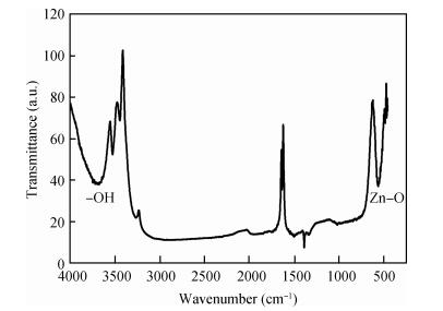
The ZnO thin films deposited onto Cu substrate with sodium thiosulfate were also examined by FTIR spectroscopy, the spectrum of which is shown in Fig. 4. From this spectrum, it can be observed apparently that there is a strong absorption band at 558 cm1 associated with the characteristic vibrational mode of ZnO. The broad absorption band centered at 3699 cm1 corresponds to the-OH group. Similar bands appeared in zinc acetate electrolyte for the deposition of ZnO thin films onto stainless steel substrate[10, 35].

Figure  4.  FTIR spectrum of ZnO thin films.

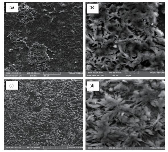
The surface morphologies of ZnO films deposited onto ITO-coated glass substrates obtained without and with sodium thiosulfate are shown in Fig. 5. The surface morphologies of deposited ZnO films prepared without sodium thiosulfate (Figs. 5(a) and 5(b)) shows non homogeneity and cracked growth surface. When sodium thiosulfate was added (Figs. 5(c) and 5(d)), we observed that the film structure is dense and uniform over a wide surface and composed of flower-like ZnO agglomerates with star-shape. Such type of star-shape and flower-like are also observed when ZnO thin films are deposited onto various substrates by different zinc salt solutions[13, 39].

Figure  5.  Color online) SEM images of ZnO films deposited onto ITO-coated glass substrates. Without sodium thiosulfate: (a) low-resolution image, (b) high-resolution image. With sodium thiosulfate: (c) low-resolution image, (d) high-resolution image.

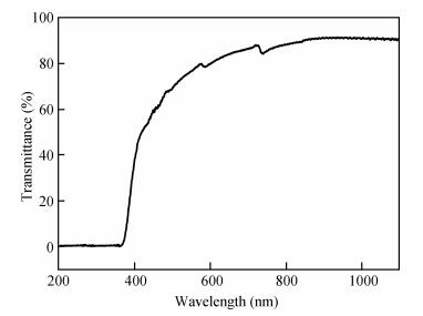
The optical transmittance spectrum of ZnO thin films deposited with sodium thiosulfate from wavelength range of, 200-1100 nm taken at room temperature is shown in Fig. 6. It was shown that the films present a high optical transmission (>80%) in the visible wavelength range, which confirms the good optical quality of the electrodeposited ZnO thin films. The absorption coefficient (α) was determined in the order of >105 cm1.

Figure  6.  Transmittance spectrum of ZnO thin films.

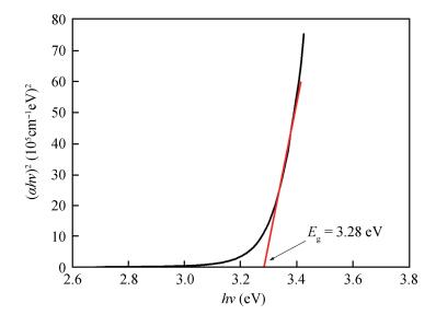
The plot of (αhν)2 versus photon energy (hν) of deposited thin films was presented in Fig. 7. It has been observed that the plots of (αhν)2 versus (hν)are linear over a wide range of photon energies indicating the direct type of transitions. The band gap of the films was determined from Tauc's formula, which is as follows Eq. (9)[40]:

Figure  7.  Plot of (αhν)2 versus hν of ZnO thin films.

(αhν)2=A(hνEg),

(9)

where α is absorption coefficient, h is Planck's constant, ν is the photon energy, A is a constant and Eg is the direct transition band gap. The optical band gap value was determined by extrapolating the linear portion of the plot of (αhν)2 versus photon energy (hν), which is illustrated in Fig. 7. The band gap of ZnO thin films was estimated to be 3.28 eV, which is in good agreement with the values reported for ZnO films by others[41, 42]. The obtained energy gap results make ZnO film a promising semiconductor material for fabrication of photovoltaic solar cells.

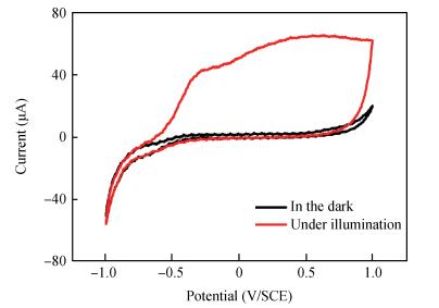
Fig. 8 shows photoelectrochemical (PEC) response of zinc oxide (ZnO) deposited with sodium thiosulfate onto ITO-coated glass substrates at 0.6 V for the solution containing 0.1 M sodium sulfate (Na2SO4), in the dark and under illumination. In the dark, there is a negligible anodic photocurrent; however, under illumination of the surface of deposited zinc oxide, we observe an important anodic photocurrent compared with in the dark. These observations suggested that the excited minority carriers (h+*) diffuse to the surface to participate in the electrochemical reaction at the electrode interface with the ions present in the electrolyte[21]. The anodic photocurrent generation represents the typical behavior of the n-type semiconductor of the ZnO thin films. This n-type semiconductor was observed when ZnO thin films were deposited onto various substrates by different zinc salt solutions[35, 43]. n-type electrical conductivity of ZnO films will be also confirmed below by Hall effect measurements.

Figure  8.  Photoelectrochemical response of ZnO thin films in the dark and under illumination.

The Hall effect measurement results showed that the ZnO thin films deposited with sodium thiosulfate have n-type conductivity with carrier concentration of-1.3 × 1017 cm3, mobility of 7.35 cm2V1s1 and a low electrical resistivity of 6.54 Ωcm. These values are in agreement with the results reported by Chen[44].

Zinc oxide (ZnO) thin films have been successfully electrodeposited onto Cu and ITO-coated glass substrates from an aqueous zinc nitrate solutions with addition of sodium thiosulfate at 90 ℃. We found that the addition of sodium thiosulfate has a strong effect on the electrochemical reaction kinetics, crystallinity and uniformity of ZnO thin films. ZnO thin films were deposited at 0.60 V for 30 min with a film thickness of about 357 nm. X-ray diffraction analysis revealed that the synthesized ZnO thin films have a hexagonal wurtzite structure. The crystallite size was estimated to be 34.69 nm. FTIR results confirmed the presence of ZnO films at peak 558 cm1. SEM images of ZnO films showed uniform, compact morphology without any cracks and consisting of flower-like ZnO agglomerates with star-shape. Photoelectrochemical measurements of ZnO thin films showed that this film behaves as a semiconductor of type n and presents high photo anodic-generated currents. These films exhibited a high optical transmission (> 80%) and high absorption coefficient (α>105 cm1) in the visible region. The optical energy band gap was found to be 3.27 eV. Hall effect measurement results confirmed that the ZnO thin films have n-type conductivity with a low electrical resistivity of 6.54 Ωcm, carrier concentration of 1.3×1017 cm3 and mobility of 7.35 cm2V1s1. Taking account of its non-toxicity and low-cost, sodium thiosulfate could be used as a promising complexing agent to prepare ZnO thin films with suitable properties for fabrication of photovoltaic solar cells.


[1]
Pawar B S, Pawar S M, Shin S W, et al. Effect of complexing agent on the properties of electrochemically deposited Cu2ZnSnS4(CZTS) thin films. Appl Surf Sci, 2010, 257: 1786 doi: 10.1016/j.apsusc.2010.09.016
[2]
Arico A S, Silvestro D, Antonucci P L, et al. Electrodeposited thin film ZnTe semiconductors for photovoltaic applications. Adv Perform Mater, 1997, 4: 115 doi: 10.1023/A:1008632602023
[3]
Sahal M, Hartiti B, Ridah A, et al. Structural, electrical and optical properties of ZnO thin films deposited by sol-gel method. Microelectron J, 2008, 39: 1425 doi: 10.1016/j.mejo.2008.06.085
[4]
Okazaki K, Kubo K, Shimogaki T, et al. Lasing characteristics of ZnO nanosheet excited by ultraviolet laser beam. Adv Mater Lett, 2011, 2(5): 354 doi: 10.5185/amlett
[5]
Singh S, Chakrabarti P. Comparison of the structural and optical properties of ZnO thin films deposited by three different methods for optoelectronic applications. Superlattices Microstruct, 2013, 64: 283 doi: 10.1016/j.spmi.2013.09.031
[6]
Li Y Y, Li Y X, Wu Y L, et al. Preparation and photoluminescent properties of zinc oxide phosphor. J Lumin, 2007, 126: 177 doi: 10.1016/j.jlumin.2006.06.012
[7]
Wang X, Ding Y, Li Z, et al. Single-crystal mesoporous ZnO thin films composed of nanowalls. Phys Chem, 2009, 113(5): 1791 http://citeseerx.ist.psu.edu/viewdoc/summary?doi=10.1.1.332.8214
[8]
Dunkel C, Graberg T, Smarsly B M, et al. Limits of ZnO electrodeposition in mesoporous tin doped indium oxide films in view of application in dye-sensitized solar cells. Mater, 2014, 7: 3291 doi: 10.3390/ma7043291
[9]
Shimogaki T, Takahashi M, Yamasaki M, et al. Catalyst-free growth of ZnO nanowires on various-oriented sapphire substrates by pulsed-laser deposition. J Semicond, 2016, 37(2): 1 http://www.cnki.com.cn/Article/CJFDTOTAL-BDTX201602005.htm
[10]
Khan Z R, Khan M S, Zulfequar M, et al. Optical and structural properties of ZnO thin films fabricated by sol-gel method. Mater Sci Appl, 2011, 2: 340 http://www.scirp.org/journal/papercitationdetails.aspx?PaperID=4774&JournalID=174
[11]
Azuma M, Ichimura M. Fabrication of ZnO thin films by the photochemical deposition method. Mate Res Bull, 2008, 43: 3537 doi: 10.1016/j.materresbull.2008.01.014
[12]
Sharma S K, Rammohan A, Sharma A. Templated one step electrodeposition of high aspect ratio n-type ZnO nanowire arrays. J Colloid Interface Sci, 2010, 344: 1 doi: 10.1016/j.jcis.2009.12.026
[13]
Kou H, Zhang X, Du Y, et al. Electrochemical synthesis of ZnO nanoflowers and nanosheets on porous Si as photoelectric materials. Appl Surf Sci, 2011, 257: 4643 doi: 10.1016/j.apsusc.2010.12.108
[14]
Qin X J, Shao G J, Lin Z. The effect of surfactant on the structure and properties of ZnO films prepared by electrodeposition. Mater Sci Eng, B, 2012, 177: 1678 doi: 10.1016/j.mseb.2012.08.012
[15]
Yıldırımand A K, Altıokka B. Effect of potential on structural, morphological and optical properties of ZnO thin films obtained by electrodeposition. Mater Sci Eng B, 2015, 120: 107 http://davidpublisher.org/Public/uploads/Contribute/55af5454a5933.pdf
[16]
Wijesundera R P, Hidaka M, Koga K, et al. Growth and characterisation of potentiostatically electrodeposited Cu2O and Cu thin films. Thin Solid Films, 2006, 500: 241 doi: 10.1016/j.tsf.2005.11.023
[17]
Yoshida T, Komatsu D, Shimokawa N, et al. Mechanism of cathodic electrodeposition of zinc oxide thin films from aqueous zinc nitrate baths. Thin Solid Films, 2004, 451: 166 https://www.researchgate.net/publication/222841633_Mechanism_of_cathodic_electrodeposition_of_zinc_oxide_thin_films_from_aqueous_zinc_nitrate_baths
[18]
Wellings J S, Chaure N B, Heavens S N, et al. Growth and characterization of electrodeposited ZnO thin films. Thin Solid Films, 2008, 516: 3893 doi: 10.1016/j.tsf.2007.07.156
[19]
Enculescu I, Matei E, Sima M, et al. Influence of polyvinylpyrolidone as an additive in electrochemical preparation of ZnO nanowires and nanostructured thin films. Surf and Interface Anal, 2008, 40: 556 doi: 10.1002/(ISSN)1096-9918
[20]
Whang T, Hsieh M, Tsai J. Lactic acid aided electrochemical deposition of c-axis preferred orientation of zinc oxide thin films: Structural and morphological features. Appl Surf Sci, 2011, 257: 9539 doi: 10.1016/j.apsusc.2011.06.058
[21]
Fathy N, Ichimura M. Electrochemical deposition of ZnO thin films from acidic solutions. J Cryst Growth, 2006, 294: 191 doi: 10.1016/j.jcrysgro.2006.07.008
[22]
Pauporte Th, Lincot D. Hydrogen peroxide oxygen precursor for zinc oxide electrodeposition Ⅱ-mechanistic aspects. J Electroanal Chem, 2001, 517: 54 doi: 10.1016/S0022-0728(01)00674-X
[23]
Li G, Dawa C, Bu Q, et al. Electrochemical self-assembly of ZnO nanoporous structures. J Phys Chem C, 2007, 111: 1919 doi: 10.1021/jp066447x
[24]
Li G, Dawa C, Bu Q, et al. Electrochemical synthesis of orientation-ordered ZnO nanorod bundles. Electrochem Commun, 2007, 9: 863 doi: 10.1016/j.elecom.2006.11.029
[25]
Inamdar A I, Sonavane A C, Sharma S K, et al. Nanocrystalline zinc oxide thin films by novel double pulse single step electro-deposition. J Alloys Compd, 2010, 495: 76 doi: 10.1016/j.jallcom.2010.01.090
[26]
Inamdar A I, Mujawar S H, Patil P S. The influences of complexing agents on growth of zinc oxide thin films from zinc acetate bath and associated kinetic parameters. Int J Electrochem Sci, 2007, 2: 797 https://www.researchgate.net/profile/P_Patil/publication/26500104_The_Influences_of_Complexing_agents_on_Growth_of_Zinc_Oxide_Thin_Films_from_Zinc_Acetate_Bath_and_Associated_Kinetic_Parameters/links/02bfe50d017f91d328000000.pdf?origin=publication_detail
[27]
Wei S, Lian J, Chen X. Effects of seed layer on the structure and property of zinc oxide thin films electrochemically deposited on ITO-coated glass. Appl Surf Sci, 2008, 254: 6605 doi: 10.1016/j.apsusc.2008.04.039
[28]
Zhang L, Chen Z, Tang Y. Low temperature cathodic electrodeposition of nanocrystalline zinc oxide thin films. Thin Solid Films, 2005, 492: 24 doi: 10.1016/j.tsf.2005.06.028
[29]
El Hichou A, Stein N, Boulanger C. Structural and spectroscopic ellipsometry characterization for electrodeposited ZnO growth at different hydrogen peroxide concentration. Thin Solid Films, 2010, 518: 4150 doi: 10.1016/j.tsf.2009.11.070
[30]
Laurent K, Wang B Q, Yu D P, et al. Structural and optical properties of electrodeposited ZnO thin films. Thin Solid Films, 2008, 517: 617 doi: 10.1016/j.tsf.2008.07.013
[31]
Gao X, Peng F, Li X, et al. Growth of highly oriented ZnO films by the two-step electrodeposition technique. J Mater Sci, 2007, 42: 9638 doi: 10.1007/s10853-007-1970-6
[32]
Abdel Haleem A M, Ichimura M. Electrochemical deposition of aluminum oxide thin films from aqueous baths. Mater Lett, 2014, 130: 26 doi: 10.1016/j.matlet.2014.05.061
[33]
Chatman Sh, Ryan B J, Poduska K M. Selective formation of Ohmic junctions and Schottky barriers with electrodeposited ZnO. Appl Phys Lett, 2008, 92: 1 http://core.ac.uk/display/19524501
[34]
Ibrahim M A M, Al Radadi R M. Role of Glycine as a complexing agent in nickel electrodeposition from acidic sulphate bath. Int J Electrochem Sci, 2015, 10: 4946 https://www.researchgate.net/publication/282159156_Role_of_Glycine_as_a_Complexing_Agent_in_Nickel_Electrodeposition_from_Acidic_Sulphate_Bath
[35]
Sulciute A, Valatka E. Electrodeposition photoelectrocatalytic activity of ZnO films on AISI 304 type steel. Mater Sci, 2012, 18(4): 318 http://www.oalib.com/paper/2315788
[36]
Ali M M. Characterization of ZnO thin films grown by chemical bath deposition. J Basra Res Sci, 2011, 37(3): 49 https://www.researchgate.net/publication/268201364_Characterization_of_ZnO_thin_films_grown_by_chemical_bath_deposition
[37]
Thool G Sh, Singh A K, Singh R S, et al. Facile synthesis of flat crystal ZnO thin films by solution growth method: a microstructural investigation. J Saudi Chem Soc, 2014, 18: 712 doi: 10.1016/j.jscs.2014.02.005
[38]
Ismail A, Abdullah M J. The structural and optical properties of ZnO thin films prepared at different RF sputtering power. J King Saud Univ Sci, 2013, 25: 209 doi: 10.1016/j.jksus.2012.12.004
[39]
Klink M J, Crouch A M. Preparation of low temperature nanostructured ZnO and RhO2 on titanium substrates, and evaluation for phenol electro-catalytic oxidation. Microchim Acta, 2009, 166: 27 doi: 10.1007/s00604-009-0157-z
[40]
Pathak T K, Kumar R, Purohit L P. Preparation and optical properties of undoped and nitrogen doped ZnO thin films by RF sputtering. Int J Chem Tech Res, 2015, 7(2): 987 https://www.researchgate.net/publication/281401796_Preparation_and_Optical_properties_of_undoped_and_Nitrogen_doped_ZnO_thin_films_by_RF_sputtering
[41]
Baviskar P K, Tan W, Zhang J, et al. Wet chemical synthesis of ZnO thin films and sensitization to light with N3 dye for solar cell application. J Phys D: Appl Phys, 2009, 42: 1
[42]
Foo K L, Kashif M, Hashim U, et al. Effect of different solvents on the structural and optical properties of zinc oxide thin films for optoelectronic applications. Ceram Int, 2014, 40: 753 doi: 10.1016/j.ceramint.2013.06.065
[43]
Chettah H, Abdi D. Effect of the electrochemical technique on nanocrysatlline ZnO electrodeposition, its structural, morphological and photoelectrochemical properties. Thin Solid Films, 2013, 537: 119 doi: 10.1016/j.tsf.2013.04.024
[44]
Chen L, Hsieh C, Zhang X. Electrical properties of CZO films prepared by ultrasonic spray pyrolysis. Mater, 2014, 7: 7304 doi: 10.3390/ma7117304
Fig. 1.  Color online) Cyclic voltammograms of the solution containing 0.1 M Zn (NO3)26H2O at pH = 5.74 and T=90 ℃, (a) without and (b) with 1.2 mM sodium thiosulfate. The potential scanning rate was 50 mV/s.

Fig. 2.  Chronoamperometry curve for the deposition of ZnO thin films.

Fig. 3.  XRD patterns of ZnO thin films deposited (a) without and (b) with sodium thiosulfate.

Fig. 4.  FTIR spectrum of ZnO thin films.

Fig. 5.  Color online) SEM images of ZnO films deposited onto ITO-coated glass substrates. Without sodium thiosulfate: (a) low-resolution image, (b) high-resolution image. With sodium thiosulfate: (c) low-resolution image, (d) high-resolution image.

Fig. 6.  Transmittance spectrum of ZnO thin films.

Fig. 7.  Plot of (αhν)2 versus hν of ZnO thin films.

Fig. 8.  Photoelectrochemical response of ZnO thin films in the dark and under illumination.

Table 1.   Electrochemical parameters obtained from cyclic voltammograms.

Table 2.   Comparison of the observed d values of ZnO films with JCPDS data (36-1451).

Table 3.   Structural parameters of ZnO thin films.

[1]
Pawar B S, Pawar S M, Shin S W, et al. Effect of complexing agent on the properties of electrochemically deposited Cu2ZnSnS4(CZTS) thin films. Appl Surf Sci, 2010, 257: 1786 doi: 10.1016/j.apsusc.2010.09.016
[2]
Arico A S, Silvestro D, Antonucci P L, et al. Electrodeposited thin film ZnTe semiconductors for photovoltaic applications. Adv Perform Mater, 1997, 4: 115 doi: 10.1023/A:1008632602023
[3]
Sahal M, Hartiti B, Ridah A, et al. Structural, electrical and optical properties of ZnO thin films deposited by sol-gel method. Microelectron J, 2008, 39: 1425 doi: 10.1016/j.mejo.2008.06.085
[4]
Okazaki K, Kubo K, Shimogaki T, et al. Lasing characteristics of ZnO nanosheet excited by ultraviolet laser beam. Adv Mater Lett, 2011, 2(5): 354 doi: 10.5185/amlett
[5]
Singh S, Chakrabarti P. Comparison of the structural and optical properties of ZnO thin films deposited by three different methods for optoelectronic applications. Superlattices Microstruct, 2013, 64: 283 doi: 10.1016/j.spmi.2013.09.031
[6]
Li Y Y, Li Y X, Wu Y L, et al. Preparation and photoluminescent properties of zinc oxide phosphor. J Lumin, 2007, 126: 177 doi: 10.1016/j.jlumin.2006.06.012
[7]
Wang X, Ding Y, Li Z, et al. Single-crystal mesoporous ZnO thin films composed of nanowalls. Phys Chem, 2009, 113(5): 1791 http://citeseerx.ist.psu.edu/viewdoc/summary?doi=10.1.1.332.8214
[8]
Dunkel C, Graberg T, Smarsly B M, et al. Limits of ZnO electrodeposition in mesoporous tin doped indium oxide films in view of application in dye-sensitized solar cells. Mater, 2014, 7: 3291 doi: 10.3390/ma7043291
[9]
Shimogaki T, Takahashi M, Yamasaki M, et al. Catalyst-free growth of ZnO nanowires on various-oriented sapphire substrates by pulsed-laser deposition. J Semicond, 2016, 37(2): 1 http://www.cnki.com.cn/Article/CJFDTOTAL-BDTX201602005.htm
[10]
Khan Z R, Khan M S, Zulfequar M, et al. Optical and structural properties of ZnO thin films fabricated by sol-gel method. Mater Sci Appl, 2011, 2: 340 http://www.scirp.org/journal/papercitationdetails.aspx?PaperID=4774&JournalID=174
[11]
Azuma M, Ichimura M. Fabrication of ZnO thin films by the photochemical deposition method. Mate Res Bull, 2008, 43: 3537 doi: 10.1016/j.materresbull.2008.01.014
[12]
Sharma S K, Rammohan A, Sharma A. Templated one step electrodeposition of high aspect ratio n-type ZnO nanowire arrays. J Colloid Interface Sci, 2010, 344: 1 doi: 10.1016/j.jcis.2009.12.026
[13]
Kou H, Zhang X, Du Y, et al. Electrochemical synthesis of ZnO nanoflowers and nanosheets on porous Si as photoelectric materials. Appl Surf Sci, 2011, 257: 4643 doi: 10.1016/j.apsusc.2010.12.108
[14]
Qin X J, Shao G J, Lin Z. The effect of surfactant on the structure and properties of ZnO films prepared by electrodeposition. Mater Sci Eng, B, 2012, 177: 1678 doi: 10.1016/j.mseb.2012.08.012
[15]
Yıldırımand A K, Altıokka B. Effect of potential on structural, morphological and optical properties of ZnO thin films obtained by electrodeposition. Mater Sci Eng B, 2015, 120: 107 http://davidpublisher.org/Public/uploads/Contribute/55af5454a5933.pdf
[16]
Wijesundera R P, Hidaka M, Koga K, et al. Growth and characterisation of potentiostatically electrodeposited Cu2O and Cu thin films. Thin Solid Films, 2006, 500: 241 doi: 10.1016/j.tsf.2005.11.023
[17]
Yoshida T, Komatsu D, Shimokawa N, et al. Mechanism of cathodic electrodeposition of zinc oxide thin films from aqueous zinc nitrate baths. Thin Solid Films, 2004, 451: 166 https://www.researchgate.net/publication/222841633_Mechanism_of_cathodic_electrodeposition_of_zinc_oxide_thin_films_from_aqueous_zinc_nitrate_baths
[18]
Wellings J S, Chaure N B, Heavens S N, et al. Growth and characterization of electrodeposited ZnO thin films. Thin Solid Films, 2008, 516: 3893 doi: 10.1016/j.tsf.2007.07.156
[19]
Enculescu I, Matei E, Sima M, et al. Influence of polyvinylpyrolidone as an additive in electrochemical preparation of ZnO nanowires and nanostructured thin films. Surf and Interface Anal, 2008, 40: 556 doi: 10.1002/(ISSN)1096-9918
[20]
Whang T, Hsieh M, Tsai J. Lactic acid aided electrochemical deposition of c-axis preferred orientation of zinc oxide thin films: Structural and morphological features. Appl Surf Sci, 2011, 257: 9539 doi: 10.1016/j.apsusc.2011.06.058
[21]
Fathy N, Ichimura M. Electrochemical deposition of ZnO thin films from acidic solutions. J Cryst Growth, 2006, 294: 191 doi: 10.1016/j.jcrysgro.2006.07.008
[22]
Pauporte Th, Lincot D. Hydrogen peroxide oxygen precursor for zinc oxide electrodeposition Ⅱ-mechanistic aspects. J Electroanal Chem, 2001, 517: 54 doi: 10.1016/S0022-0728(01)00674-X
[23]
Li G, Dawa C, Bu Q, et al. Electrochemical self-assembly of ZnO nanoporous structures. J Phys Chem C, 2007, 111: 1919 doi: 10.1021/jp066447x
[24]
Li G, Dawa C, Bu Q, et al. Electrochemical synthesis of orientation-ordered ZnO nanorod bundles. Electrochem Commun, 2007, 9: 863 doi: 10.1016/j.elecom.2006.11.029
[25]
Inamdar A I, Sonavane A C, Sharma S K, et al. Nanocrystalline zinc oxide thin films by novel double pulse single step electro-deposition. J Alloys Compd, 2010, 495: 76 doi: 10.1016/j.jallcom.2010.01.090
[26]
Inamdar A I, Mujawar S H, Patil P S. The influences of complexing agents on growth of zinc oxide thin films from zinc acetate bath and associated kinetic parameters. Int J Electrochem Sci, 2007, 2: 797 https://www.researchgate.net/profile/P_Patil/publication/26500104_The_Influences_of_Complexing_agents_on_Growth_of_Zinc_Oxide_Thin_Films_from_Zinc_Acetate_Bath_and_Associated_Kinetic_Parameters/links/02bfe50d017f91d328000000.pdf?origin=publication_detail
[27]
Wei S, Lian J, Chen X. Effects of seed layer on the structure and property of zinc oxide thin films electrochemically deposited on ITO-coated glass. Appl Surf Sci, 2008, 254: 6605 doi: 10.1016/j.apsusc.2008.04.039
[28]
Zhang L, Chen Z, Tang Y. Low temperature cathodic electrodeposition of nanocrystalline zinc oxide thin films. Thin Solid Films, 2005, 492: 24 doi: 10.1016/j.tsf.2005.06.028
[29]
El Hichou A, Stein N, Boulanger C. Structural and spectroscopic ellipsometry characterization for electrodeposited ZnO growth at different hydrogen peroxide concentration. Thin Solid Films, 2010, 518: 4150 doi: 10.1016/j.tsf.2009.11.070
[30]
Laurent K, Wang B Q, Yu D P, et al. Structural and optical properties of electrodeposited ZnO thin films. Thin Solid Films, 2008, 517: 617 doi: 10.1016/j.tsf.2008.07.013
[31]
Gao X, Peng F, Li X, et al. Growth of highly oriented ZnO films by the two-step electrodeposition technique. J Mater Sci, 2007, 42: 9638 doi: 10.1007/s10853-007-1970-6
[32]
Abdel Haleem A M, Ichimura M. Electrochemical deposition of aluminum oxide thin films from aqueous baths. Mater Lett, 2014, 130: 26 doi: 10.1016/j.matlet.2014.05.061
[33]
Chatman Sh, Ryan B J, Poduska K M. Selective formation of Ohmic junctions and Schottky barriers with electrodeposited ZnO. Appl Phys Lett, 2008, 92: 1 http://core.ac.uk/display/19524501
[34]
Ibrahim M A M, Al Radadi R M. Role of Glycine as a complexing agent in nickel electrodeposition from acidic sulphate bath. Int J Electrochem Sci, 2015, 10: 4946 https://www.researchgate.net/publication/282159156_Role_of_Glycine_as_a_Complexing_Agent_in_Nickel_Electrodeposition_from_Acidic_Sulphate_Bath
[35]
Sulciute A, Valatka E. Electrodeposition photoelectrocatalytic activity of ZnO films on AISI 304 type steel. Mater Sci, 2012, 18(4): 318 http://www.oalib.com/paper/2315788
[36]
Ali M M. Characterization of ZnO thin films grown by chemical bath deposition. J Basra Res Sci, 2011, 37(3): 49 https://www.researchgate.net/publication/268201364_Characterization_of_ZnO_thin_films_grown_by_chemical_bath_deposition
[37]
Thool G Sh, Singh A K, Singh R S, et al. Facile synthesis of flat crystal ZnO thin films by solution growth method: a microstructural investigation. J Saudi Chem Soc, 2014, 18: 712 doi: 10.1016/j.jscs.2014.02.005
[38]
Ismail A, Abdullah M J. The structural and optical properties of ZnO thin films prepared at different RF sputtering power. J King Saud Univ Sci, 2013, 25: 209 doi: 10.1016/j.jksus.2012.12.004
[39]
Klink M J, Crouch A M. Preparation of low temperature nanostructured ZnO and RhO2 on titanium substrates, and evaluation for phenol electro-catalytic oxidation. Microchim Acta, 2009, 166: 27 doi: 10.1007/s00604-009-0157-z
[40]
Pathak T K, Kumar R, Purohit L P. Preparation and optical properties of undoped and nitrogen doped ZnO thin films by RF sputtering. Int J Chem Tech Res, 2015, 7(2): 987 https://www.researchgate.net/publication/281401796_Preparation_and_Optical_properties_of_undoped_and_Nitrogen_doped_ZnO_thin_films_by_RF_sputtering
[41]
Baviskar P K, Tan W, Zhang J, et al. Wet chemical synthesis of ZnO thin films and sensitization to light with N3 dye for solar cell application. J Phys D: Appl Phys, 2009, 42: 1
[42]
Foo K L, Kashif M, Hashim U, et al. Effect of different solvents on the structural and optical properties of zinc oxide thin films for optoelectronic applications. Ceram Int, 2014, 40: 753 doi: 10.1016/j.ceramint.2013.06.065
[43]
Chettah H, Abdi D. Effect of the electrochemical technique on nanocrysatlline ZnO electrodeposition, its structural, morphological and photoelectrochemical properties. Thin Solid Films, 2013, 537: 119 doi: 10.1016/j.tsf.2013.04.024
[44]
Chen L, Hsieh C, Zhang X. Electrical properties of CZO films prepared by ultrasonic spray pyrolysis. Mater, 2014, 7: 7304 doi: 10.3390/ma7117304
1

Review of recent progresses on flexible oxide semiconductor thin film transistors based on atomic layer deposition processes

Jiazhen Sheng, Ki-Lim Han, TaeHyun Hong, Wan-Ho Choi, Jin-Seong Park, et al.

Journal of Semiconductors, 2018, 39(1): 011008. doi: 10.1088/1674-4926/39/1/011008

2

Substrate temperature dependent studies on properties of chemical spray pyrolysis deposited CdS thin films for solar cell applications

Kiran Diwate, Amit Pawbake, Sachin Rondiya, Rupali Kulkarni, Ravi Waykar, et al.

Journal of Semiconductors, 2017, 38(2): 023001. doi: 10.1088/1674-4926/38/2/023001

3

SnS thin films deposited by chemical bath deposition, dip coating and SILAR techniques

Sunil H. Chaki, Mahesh D. Chaudhary, M. P. Deshpande

Journal of Semiconductors, 2016, 37(5): 053001. doi: 10.1088/1674-4926/37/5/053001

4

The calculation of band gap energy in zinc oxide films

Ali Arif, Okba Belahssen, Salim Gareh, Said Benramache

Journal of Semiconductors, 2015, 36(1): 013001. doi: 10.1088/1674-4926/36/1/013001

5

Progress in complementary metal-oxide-semiconductor silicon photonics and optoelectronic integrated circuits

Hongda Chen, Zan Zhang, Beiju Huang, Luhong Mao, Zanyun Zhang, et al.

Journal of Semiconductors, 2015, 36(12): 121001. doi: 10.1088/1674-4926/36/12/121001

6

First-principles calculations of Mg2X (X = Si, Ge, Sn) semiconductors with the calcium fluorite structure

Sandong Guo

Journal of Semiconductors, 2015, 36(5): 053002. doi: 10.1088/1674-4926/36/5/053002

7

Structural, optical and electrical properties of zinc oxide thin films deposited by a spray pyrolysis technique

Yacine Aoun, Boubaker Benhaoua, Brahim Gasmi, Said Benramache

Journal of Semiconductors, 2015, 36(1): 013002. doi: 10.1088/1674-4926/36/1/013002

8

Optical properties of electrochemically synthesized polypyrrole thin films: the electrolyte effect

J.V. Thombare, S.K. Shinde, G.M. Lohar, U.M. Chougale, S.S. Dhasade, et al.

Journal of Semiconductors, 2014, 35(6): 063001. doi: 10.1088/1674-4926/35/6/063001

9

Effect of band gap energy on the electrical conductivity in doped ZnO thin film

Said Benramache, Okba Belahssen, Hachemi Ben Temam

Journal of Semiconductors, 2014, 35(7): 073001. doi: 10.1088/1674-4926/35/7/073001

10

Synthesis of In2S3 thin films by spray pyrolysis from precursors with different[S]/[In] ratios

Thierno Sall, A. Nafidi, Bernabé Marí Soucase, Miguel Mollar, Bouchaib Hartitti, et al.

Journal of Semiconductors, 2014, 35(6): 063002. doi: 10.1088/1674-4926/35/6/063002

11

The effect of solution concentration on the physical and electrochemical properties of vanadium oxide films deposited by spray pyrolysis

M. Mousavi, A. Kompany, N. Shahtahmasebi, M.M. Bagheri-Mohagheghi

Journal of Semiconductors, 2013, 34(10): 103001. doi: 10.1088/1674-4926/34/10/103001

12

Solar light assisted photocatalysis of water using a zinc oxide semiconductor

S.S. Shinde, C.H. Bhosale, K.Y. Rajpure

Journal of Semiconductors, 2013, 34(4): 043002. doi: 10.1088/1674-4926/34/4/043002

13

Photoconductivity and surface chemical analysis of ZnO thin films deposited by solution-processing techniques for nano and microstructure fabrication

V.K. Dwivedi, P. Srivastava, G. Vijaya Prakash

Journal of Semiconductors, 2013, 34(3): 033001. doi: 10.1088/1674-4926/34/3/033001

14

Correlation between electrical conductivity-optical band gap energy and precursor molarities ultrasonic spray deposition of ZnO thin films

Said Benramache, Okba Belahssen, Abderrazak Guettaf, Ali Arif

Journal of Semiconductors, 2013, 34(11): 113001. doi: 10.1088/1674-4926/34/11/113001

15

Dielectric response and electric properties of organic semiconducting phthalocyanine thin films

A. M. Saleh, S. M. Hraibat, R. M-L. Kitaneh, M. M. Abu-Samreh, S. M. Musameh, et al.

Journal of Semiconductors, 2012, 33(8): 082002. doi: 10.1088/1674-4926/33/8/082002

16

A nanostructured copper telluride thin film grown at room temperature by an electrodeposition method

S. S. Dhasade, S. H. Han, V. J. Fulari

Journal of Semiconductors, 2012, 33(9): 093002. doi: 10.1088/1674-4926/33/9/093002

17

Local charge neutrality condition, Fermi level and majority carrier density of a semiconductor with multiple localized multi-level intrinsic/impurity defects

Ken K. Chin

Journal of Semiconductors, 2011, 32(11): 112001. doi: 10.1088/1674-4926/32/11/112001

18

Synthesis of organic semiconductor hexadecachloro zinc phthalocyanine and its gas sensitivity

Shi Yunbo, Lei Tingping, Li Zan, Xiu Debin, Zhao Wenjie, et al.

Journal of Semiconductors, 2009, 30(3): 034009. doi: 10.1088/1674-4926/30/3/034009

19

Sensitive properties of In-based compound semiconductor oxide to Cl2 gas

Zhao Wenjie, Shi Yunbo, Xiu Debin, Lei Tingping, Feng Qiaohua, et al.

Journal of Semiconductors, 2009, 30(3): 034010. doi: 10.1088/1674-4926/30/3/034010

20

Electronic Structure of Semiconductor Nanocrystals

Li Jingbo, Wang Linwang, Wei Suhuai

Chinese Journal of Semiconductors , 2006, 27(2): 191-196.

1. Zyoud, S.H., Omar, A.F. Investigating the enhanced UV photoresponse of Cu-doped ZnO thin films synthesized via laser assisted chemical bath growth. Applied Physics A: Materials Science and Processing, 2024, 130(11): 839. doi:10.1007/s00339-024-08014-4
2. Nimalan, T., Begam, M.R. A Comprehensive Review of Preparation Methods, Parameters and Deposition Analysis of CuO/ZnO Thin Films. International Journal of Thin Film Science and Technology, 2024, 13(3): 213-224. doi:10.18576/ijtfst/130306
3. Amudhavalli, B., Mariappan, R., Prasath, M. Synthesis chemical methods for deposition of ZnO, CdO and CdZnO thin films to facilitate further research. Journal of Alloys and Compounds, 2022. doi:10.1016/j.jallcom.2022.166511
4. Ibrahim, A.S., Alex, K.V., Latha, M.B. et al. Effect of the thickness on the photocatalytic and the photocurrent properties of ZnO films deposited by spray pyrolysis. Discover Materials, 2022, 2(1): 10. doi:10.1007/s43939-022-00031-5
5. Namawardana, D.G.K.K., Wanigasekara, R.M.G., Wanninayake, W.T.M.A.P.K. et al. Fabrication of inverted organic solar cells on stainless steel substrate with electrodeposited and spin coated ZnO buffer layers. Journal of Polymer Engineering, 2022, 42(3): 233-242. doi:10.1515/polyeng-2021-0280
6. Jose, L.M., Raj, R.S.A., Sajan, D. et al. Adsorption and photocatalytic activity of biosynthesised ZnO nanoparticles using Aloe Vera leaf extract. Nano Express, 2021, 2(1): 010039. doi:10.1088/2632-959X/abeec6
7. Liau, L.C.-K., Kuo, P.-W. Characterization of ZnO-Cu2O crystal films by electrochemical codeposition. Journal of Solid State Electrochemistry, 2020, 24(2): 421-429. doi:10.1007/s10008-019-04411-5
8. Francis, M., Lakshmi, M. Silver doped sputtered ZnO thin films. AIP Conference Proceedings, 2019. doi:10.1063/1.5130340
9. Lakhdari, M., Habelhames, F. Morphological and structural control of pulse electrodeposited ZnO thin films and its influence on the photoelectrocatalytic degradation of methyl orange. Journal of Materials Science: Materials in Electronics, 2019, 30(6): 6107-6115. doi:10.1007/s10854-019-00912-1
  • Search

    Advanced Search >>

    GET CITATION

    Hassiba Rahal, Rafiaa Kihal, Abed Mohamed Affoune, Mokhtar Ghers, Faycal Djazi. Electrodeposition and characterization of ZnO thin films using sodium thiosulfate as an additive for photovoltaic solar cells[J]. Journal of Semiconductors, 2017, 38(5): 053002. doi: 10.1088/1674-4926/38/5/053002
    H Rahal, R Kihal, A M Affoune, M Ghers, F Djazi. Electrodeposition and characterization of ZnO thin films using sodium thiosulfate as an additive for photovoltaic solar cells[J]. J. Semicond., 2017, 38(5): 053002. doi: 10.1088/1674-4926/38/5/053002.
    shu

    Export: BibTex EndNote

    Article Metrics

    Article views: 3944 Times PDF downloads: 89 Times Cited by: 9 Times

    History

    Received: 12 October 2016 Revised: 15 December 2016 Online: Published: 01 May 2017

    Catalog

      Email This Article

      User name:
      Email:*请输入正确邮箱
      Code:*验证码错误
      Hassiba Rahal, Rafiaa Kihal, Abed Mohamed Affoune, Mokhtar Ghers, Faycal Djazi. Electrodeposition and characterization of ZnO thin films using sodium thiosulfate as an additive for photovoltaic solar cells[J]. Journal of Semiconductors, 2017, 38(5): 053002. doi: 10.1088/1674-4926/38/5/053002 ****H Rahal, R Kihal, A M Affoune, M Ghers, F Djazi. Electrodeposition and characterization of ZnO thin films using sodium thiosulfate as an additive for photovoltaic solar cells[J]. J. Semicond., 2017, 38(5): 053002. doi: 10.1088/1674-4926/38/5/053002.
      Citation:
      Hassiba Rahal, Rafiaa Kihal, Abed Mohamed Affoune, Mokhtar Ghers, Faycal Djazi. Electrodeposition and characterization of ZnO thin films using sodium thiosulfate as an additive for photovoltaic solar cells[J]. Journal of Semiconductors, 2017, 38(5): 053002. doi: 10.1088/1674-4926/38/5/053002 ****
      H Rahal, R Kihal, A M Affoune, M Ghers, F Djazi. Electrodeposition and characterization of ZnO thin films using sodium thiosulfate as an additive for photovoltaic solar cells[J]. J. Semicond., 2017, 38(5): 053002. doi: 10.1088/1674-4926/38/5/053002.

      Electrodeposition and characterization of ZnO thin films using sodium thiosulfate as an additive for photovoltaic solar cells

      DOI: 10.1088/1674-4926/38/5/053002
      Funds:

      Project supported by the Algerian Ministry of Higher Education and Scientific Research, Algeria (No. J0101520090018)

      the Algerian Ministry of Higher Education and Scientific Research, Algeria J0101520090018

      More Information
      • Corresponding author: Abed Mohamed Affoune Email: affoune2@yahoo.fr
      • Received Date: 2016-10-12
      • Revised Date: 2016-12-15
      • Published Date: 2017-05-01

      Catalog

        /

        DownLoad:  Full-Size Img  PowerPoint
        Return
        Return