


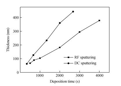
Fig. 1.
The thickness of deposited Ni24.9Cr72.5Si2.6 thin films as a function of deposition time.
SEMICONDUCTOR MATERIALS
Bing Cheng, Yijun Yin, Jianqiang Han and Jie Zhang
Corresponding author: Jianqiang Han, Email: hjqsmx@163.com
Abstract: The temperature coefficient of resistance (abbreviated as TCR) of thin film resistors on some sensor chips, such as thermal converters, should be less than several ppm/℃.However, the TCR of reported thin films is larger than 5 ppm/℃.In this paper, Ni24.9Cr72.5Si2.6 films are deposited on silicon dioxide film by DC and RF magnetron sputtering.Then as-deposited films are annealed at 450℃ under different durations in N2 atmosphere. The sheet resistance of thin films with various thickness and annealing time are measured by the four probe resistivity test system at temperature of 20, 50, 100, 150, and 200℃ and then the TCR of thin films are calculated. Experimental results show that the film with the TCR of only-0.86 ppm/℃ can be achieved by RF magnetron sputtering and appropriate annealing conditions.
Keywords: magnetron sputtering, NiCrSi thin film, sheet resistance, temperature coefficient of resistance, thermal converter
| [1] |
Van den Broek J J, Donkers J J T M, van der Rijt R A F, et al.Metal film precision resistors: resistive metal films and a new resistor concept. Philips J Res, 1998, 51: 429 doi: 10.1016/S0165-5817(98)00013-8
|
| [2] |
Vinayak S, Vyas H P, Muraleedharan K, et al. Ni-Cr thin film resistor fabrication for GaAs monolithic microwave integrated circuits. Thin Solid Films, 2006, 514: 52 doi: 10.1016/j.tsf.2006.02.025
|
| [3] |
Vinayak S, Vyas H P, Vankar V D. Microstructure and electrical characteristics of Ni-Cr thin films. Thin Solid Films, 2007, 515: 136 http://www.sciencedirect.com/science/article/pii/S0040609007003197
|
| [4] |
Schippel E. The influence of silicon on properties of deposited Ni-Cr films. Thin Solid Films, 1986, 144: 21 doi: 10.1016/0040-6090(86)90066-0
|
| [5] |
Gawalek W. Resistance temperature coefficient of resistance and long-term stability of annealed thin Ni-Cr-Si films. Thin Solid Films, 1984, 116: 205 doi: 10.1016/0040-6090(84)90430-9
|
| [6] |
Lee B J, Park G B, Kim J I, et al. The effect of the process parameters on the electrical properties of Ni-Cr-Si alloy thin resistor films. Annual Report Conference on Electrical Insulation and Dielectric Phenomena, 2002: 72 https://www.researchgate.net/publication/3976899_The_effect_of_the_process_parameters_on_the_electrical_properties_of_Ni-Cr-Si_alloy_thin_resistor_films
|
| [7] |
Zhang Y Q, Dong X P D, Wu J S. Microstructure and electrical characteristics of Cr-Si-Ni films deposited on glass and Si (100) substrates by RF magnetron sputtering. Mater Sci Eng B, 2004, 113: 154 doi: 10.1016/S0921-5107(04)00402-7
|
| [8] |
Chiang C S, Lee W H, Jap F. Investigation into microstructural and electrical characteristics of Ni-Cr-Si thin-film resistors deposited in Al2O3 substrate using DC and RF magnetron sputtering. International Symposium on Next-Generation Electronics (ISNE), 2004: 1
|
| [9] |
Cheng H Y, Chen Y C, Li P J, et al. Effect of annealing process on the properties of Ni (55%) Cr (40%) Si (5%) thin-film resistors. Materials, 2015, 8: 6752 doi: 10.3390/ma8105338
|
| [10] |
Klonz M, Laiz H, Kessler E. Development of thin-film multijunction thermal converters at PTB/IPHT. IEEE Trans Instrum Meas, 2001, 50: 1490 doi: 10.1109/19.982933
|
| [11] |
Yasutaka A, Hiroyuki F, Koji S, et al. Low-frequency characteristics of a thin-film multijunction thermal converter under vacuum. CPEM Digest (Conference on Precision Electromagnetic Measurements), 2014: 50
|
| [12] |
Yasutaka A, Hiroyuki F, Koji S, et al. Improvements in the lowfrequency characteristic and sensitivity of a thin-film multijunction thermal converter in vacuum. IEEE Trans Instrum Meas, 2015, 64: 1570 doi: 10.1109/TIM.2014.2385133
|
| [13] |
Hiroyuki F. Development of thin-film multijunction thermal converters with a novel structure. IEEE Trans Instrum Meas, 2011, 60: 2725 doi: 10.1109/TIM.2010.2103412
|
| [14] |
Zhaohui Q, Dieter M. Comparison of radio-frequency and directcurrent magnetron sputtered thin In2O3:Sn films. Thin Solid Films, 2005, 484: 146 doi: 10.1016/j.tsf.2005.02.006
|
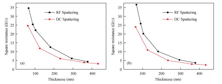
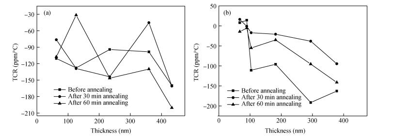
Table 1. Sheet resistance and TCR of Ni24.9Cr72.5Si2.6 films deposited by DC/RF magnetron sputtering.

|
| [1] |
Van den Broek J J, Donkers J J T M, van der Rijt R A F, et al.Metal film precision resistors: resistive metal films and a new resistor concept. Philips J Res, 1998, 51: 429 doi: 10.1016/S0165-5817(98)00013-8
|
| [2] |
Vinayak S, Vyas H P, Muraleedharan K, et al. Ni-Cr thin film resistor fabrication for GaAs monolithic microwave integrated circuits. Thin Solid Films, 2006, 514: 52 doi: 10.1016/j.tsf.2006.02.025
|
| [3] |
Vinayak S, Vyas H P, Vankar V D. Microstructure and electrical characteristics of Ni-Cr thin films. Thin Solid Films, 2007, 515: 136 http://www.sciencedirect.com/science/article/pii/S0040609007003197
|
| [4] |
Schippel E. The influence of silicon on properties of deposited Ni-Cr films. Thin Solid Films, 1986, 144: 21 doi: 10.1016/0040-6090(86)90066-0
|
| [5] |
Gawalek W. Resistance temperature coefficient of resistance and long-term stability of annealed thin Ni-Cr-Si films. Thin Solid Films, 1984, 116: 205 doi: 10.1016/0040-6090(84)90430-9
|
| [6] |
Lee B J, Park G B, Kim J I, et al. The effect of the process parameters on the electrical properties of Ni-Cr-Si alloy thin resistor films. Annual Report Conference on Electrical Insulation and Dielectric Phenomena, 2002: 72 https://www.researchgate.net/publication/3976899_The_effect_of_the_process_parameters_on_the_electrical_properties_of_Ni-Cr-Si_alloy_thin_resistor_films
|
| [7] |
Zhang Y Q, Dong X P D, Wu J S. Microstructure and electrical characteristics of Cr-Si-Ni films deposited on glass and Si (100) substrates by RF magnetron sputtering. Mater Sci Eng B, 2004, 113: 154 doi: 10.1016/S0921-5107(04)00402-7
|
| [8] |
Chiang C S, Lee W H, Jap F. Investigation into microstructural and electrical characteristics of Ni-Cr-Si thin-film resistors deposited in Al2O3 substrate using DC and RF magnetron sputtering. International Symposium on Next-Generation Electronics (ISNE), 2004: 1
|
| [9] |
Cheng H Y, Chen Y C, Li P J, et al. Effect of annealing process on the properties of Ni (55%) Cr (40%) Si (5%) thin-film resistors. Materials, 2015, 8: 6752 doi: 10.3390/ma8105338
|
| [10] |
Klonz M, Laiz H, Kessler E. Development of thin-film multijunction thermal converters at PTB/IPHT. IEEE Trans Instrum Meas, 2001, 50: 1490 doi: 10.1109/19.982933
|
| [11] |
Yasutaka A, Hiroyuki F, Koji S, et al. Low-frequency characteristics of a thin-film multijunction thermal converter under vacuum. CPEM Digest (Conference on Precision Electromagnetic Measurements), 2014: 50
|
| [12] |
Yasutaka A, Hiroyuki F, Koji S, et al. Improvements in the lowfrequency characteristic and sensitivity of a thin-film multijunction thermal converter in vacuum. IEEE Trans Instrum Meas, 2015, 64: 1570 doi: 10.1109/TIM.2014.2385133
|
| [13] |
Hiroyuki F. Development of thin-film multijunction thermal converters with a novel structure. IEEE Trans Instrum Meas, 2011, 60: 2725 doi: 10.1109/TIM.2010.2103412
|
| [14] |
Zhaohui Q, Dieter M. Comparison of radio-frequency and directcurrent magnetron sputtered thin In2O3:Sn films. Thin Solid Films, 2005, 484: 146 doi: 10.1016/j.tsf.2005.02.006
|


Article views: 4095 Times PDF downloads: 53 Times Cited by: 0 Times
Received: 20 September 2016 Revised: 14 November 2016 Online: Published: 01 May 2017
| Citation: |
Bing Cheng, Yijun Yin, Jianqiang Han, Jie Zhang. The TCR of Ni24.9Cr72.5Si2.6 thin films deposited by DC and RF magnetronsputtering[J]. Journal of Semiconductors, 2017, 38(5): 053005. doi: 10.1088/1674-4926/38/5/053005
****
B Cheng, Y J Yin, J Q Han, J Zhang. The TCR of Ni24.9Cr72.5Si2.6 thin films deposited by DC and RF magnetronsputtering[J]. J. Semicond., 2017, 38(5): 053005. doi: 10.1088/1674-4926/38/5/053005.

|
| [1] |
Van den Broek J J, Donkers J J T M, van der Rijt R A F, et al.Metal film precision resistors: resistive metal films and a new resistor concept. Philips J Res, 1998, 51: 429 doi: 10.1016/S0165-5817(98)00013-8
|
| [2] |
Vinayak S, Vyas H P, Muraleedharan K, et al. Ni-Cr thin film resistor fabrication for GaAs monolithic microwave integrated circuits. Thin Solid Films, 2006, 514: 52 doi: 10.1016/j.tsf.2006.02.025
|
| [3] |
Vinayak S, Vyas H P, Vankar V D. Microstructure and electrical characteristics of Ni-Cr thin films. Thin Solid Films, 2007, 515: 136 http://www.sciencedirect.com/science/article/pii/S0040609007003197
|
| [4] |
Schippel E. The influence of silicon on properties of deposited Ni-Cr films. Thin Solid Films, 1986, 144: 21 doi: 10.1016/0040-6090(86)90066-0
|
| [5] |
Gawalek W. Resistance temperature coefficient of resistance and long-term stability of annealed thin Ni-Cr-Si films. Thin Solid Films, 1984, 116: 205 doi: 10.1016/0040-6090(84)90430-9
|
| [6] |
Lee B J, Park G B, Kim J I, et al. The effect of the process parameters on the electrical properties of Ni-Cr-Si alloy thin resistor films. Annual Report Conference on Electrical Insulation and Dielectric Phenomena, 2002: 72 https://www.researchgate.net/publication/3976899_The_effect_of_the_process_parameters_on_the_electrical_properties_of_Ni-Cr-Si_alloy_thin_resistor_films
|
| [7] |
Zhang Y Q, Dong X P D, Wu J S. Microstructure and electrical characteristics of Cr-Si-Ni films deposited on glass and Si (100) substrates by RF magnetron sputtering. Mater Sci Eng B, 2004, 113: 154 doi: 10.1016/S0921-5107(04)00402-7
|
| [8] |
Chiang C S, Lee W H, Jap F. Investigation into microstructural and electrical characteristics of Ni-Cr-Si thin-film resistors deposited in Al2O3 substrate using DC and RF magnetron sputtering. International Symposium on Next-Generation Electronics (ISNE), 2004: 1
|
| [9] |
Cheng H Y, Chen Y C, Li P J, et al. Effect of annealing process on the properties of Ni (55%) Cr (40%) Si (5%) thin-film resistors. Materials, 2015, 8: 6752 doi: 10.3390/ma8105338
|
| [10] |
Klonz M, Laiz H, Kessler E. Development of thin-film multijunction thermal converters at PTB/IPHT. IEEE Trans Instrum Meas, 2001, 50: 1490 doi: 10.1109/19.982933
|
| [11] |
Yasutaka A, Hiroyuki F, Koji S, et al. Low-frequency characteristics of a thin-film multijunction thermal converter under vacuum. CPEM Digest (Conference on Precision Electromagnetic Measurements), 2014: 50
|
| [12] |
Yasutaka A, Hiroyuki F, Koji S, et al. Improvements in the lowfrequency characteristic and sensitivity of a thin-film multijunction thermal converter in vacuum. IEEE Trans Instrum Meas, 2015, 64: 1570 doi: 10.1109/TIM.2014.2385133
|
| [13] |
Hiroyuki F. Development of thin-film multijunction thermal converters with a novel structure. IEEE Trans Instrum Meas, 2011, 60: 2725 doi: 10.1109/TIM.2010.2103412
|
| [14] |
Zhaohui Q, Dieter M. Comparison of radio-frequency and directcurrent magnetron sputtered thin In2O3:Sn films. Thin Solid Films, 2005, 484: 146 doi: 10.1016/j.tsf.2005.02.006
|

 WeChat ID
Journal of Semiconductors © 2017 All Rights Reserved 京ICP备05085259号-2

 DownLoad:

