


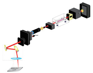
Fig. 1.
Principle of laser micro processing.
SEMICONDUCTOR TECHNOLOGY
Xinling Meng1, 2, Luqi Tao1, 2, Zhaolin Liu1, 2, Yi Yang1, 2 and Tianling Ren1, 2,
Corresponding author: Ren Tianling, Email: rentl@tsinghua.edu.cn
Abstract: The electromagnetic shielding film has drawn much attention due to its wide applications in the integrated circuit package, which demands a high surface quality of epoxy resin. However, gaseous Cu will splash and adhere to epoxy resin surface when the Cu layer in PCB receives enough energy in the process of laser cutting, which has a negative effect on the quality of the shielding film. Laser polishing technology can solve this problem and it can effectively improve the quality of epoxy resin surface. The paper studies the mechanism of Cu powder spraying on the compound surface by 355 nm ultraviolet (UV) laser, including the parameters of laser polishing process and the remains of Cu content on compound surface. The results show that minimal Cu content can be realized with a scanning speed of 700 mm/s, a laser frequency of 50 kHz and the distance between laser focus and product top surface of -1.3 mm. This result is important to obtain an epoxy resin surface with high quality.
Keywords: laser polishing, epoxy resin, surface quality
| [1] |
Yu X J, Zhang X Y, Fan W, et al. Technology of electroles copper plating on ABS plastics. Electroplating & Finishing, 2007, 26(5): 10 http://en.cnki.com.cn/Article_en/CJFDTOTAL-DDTL200705004.htm
|
| [2] |
Domenech S C, Lima J E, Drago V, et al. Electroless plating of nickel-phosphorous on surface-modified poly (ethylene terephthalate) films. Appl Surf Sci, 2003, 220(1): 238 http://www.sciencedirect.com/science/article/pii/S0169433203008158
|
| [3] |
Van Eck W. Electromagnetic radiation from video display units: an eavesdropping risk. Computer & Security, 1985, (4): 269 http://www.sciencedirect.com/science/article/pii/016740488590046X
|
| [4] |
Laguarta F L. Laser application for optical glass polishing. Opt Soc Am, 1997, 56(24): 352 http://opticalengineering.spiedigitallibrary.org/article.aspx?articleid=1075148
|
| [5] |
Dai Y T, Xu G, Tong X L. Deep UV laser etching of GaN epilayers grown on sapphire substrate. J Mater Process Technol, 2012, 212(2): 492 doi: 10.1016/j.jmatprotec.2011.08.022
|
| [6] |
Shi E G, Zhao B. Modeling of chemical mechanical polishing with soft pads. Appl Phys A, 1998, 67: 249 doi: 10.1007/s003390050766
|
| [7] |
Hanh P O. The 300 mm silicon wafer-a cost and technology challenge. Microelectron Eng, 2001, 56(1/2): 3 https://www.researchgate.net/publication/223589930_The_300_mm_silicon_wafer_-_A_cost_and_technology_challenge
|
| [8] |
Steigerwald J M, Murka S P, Gutmann R J, et al. Chemical processes in the chemical mechanical polishing of copper. Mater Chem Phys, 1995, 41(3): 217 doi: 10.1016/0254-0584(95)01516-7
|
| [9] |
Yoshiki H, Hashimoto K, Fujishima A. Reaction mechanism of electroless metal deposition using ZnO thin film (Ⅰ): process of catalyst formation. Electrochem Soc, 1995, 142(2): 428 doi: 10.1149/1.2044049
|
| [10] |
Kretz F. The electroless deposition of nickel on SiC particles for aluminum matrix composites. Surf Coat Technol, 2004, 180/181: 575 doi: 10.1016/j.surfcoat.2003.10.150
|
| [11] |
Lindsay, Deborah J, Feldstein, et al. Activators for colloidal catalysts in electroless plating processes. US Patent, 4820547, 1988-06-27 http://www.freepatentsonline.com/4820547.html
|
| [12] |
Takino H, Shibata N, Itoh H, et al. Fabrication of optics by use of plasma chemical vaporization machining with a pipe electrode. Appl Opt, 2002, 41(19): 3971 doi: 10.1364/AO.41.003971
|
| [13] |
Bollinger D, Gallatin G, Samuels J, et al. Rapid, Noncontact optical figuring of aspheric surfaces with plasma assisted chemical etching (PACE) SPIE. Adv Opt Manufact Testing, 1990, 1333(23): 44 doi: 10.1117/12.22788
|
| [14] |
Zarowin C B. A comparison using surface evolution theory of the smoothing and figuring of optics by plasma assisted chemical etching and ion milling. SPIE, 1991(1618): 22 doi: 10.1117/12.58038
|
| [15] |
Solodlii E N, Solodkii N F. Reasond for tinting of corundum ceramics (a review). Glass and Ceramics, 2001, 58(11): 391 doi: 10.1023/A%3A1014910425932
|
| [16] |
Kacara E, Mutlua M, Akman E, et al. Characterization of the drilling alumina ceramic using Nd-YAG pulsed laser. J Mater Processing Technol, 2009, 209(4): 2008 doi: 10.1016/j.jmatprotec.2008.04.049
|
| [17] |
Hanon M M, Akman E, Genc O B, et al. Experimental and theoretical investigation of the drilling of alumina ceramic using Nd-YAG pulsed laser. Opt Laser Technol, 2012, 44(4): 913 doi: 10.1016/j.optlastec.2011.11.010
|
| [18] |
Brinksmeier E, Riemer O, Gessenharter A, et al. Polishing of structured molds. CIRP Annals-Manufact Technol, 2004, 53(1): 247 doi: 10.1016/S0007-8506(07)60690-8
|
| [19] |
Hua M, Shao T, Hong Y T, et al. Influence of pulse duration on the surface morphology of ASSAB DF-2(AISI-01) cold work steel treated by YAG laser. Surf Coat Technol, 2004, 185(2): 127 http://www.sciencedirect.com/science/article/pii/S0257897204000349
|
| [20] |
Trtica M, Gakovic B, Batani D, et al. Surface modifications of a titanium implant by a picosecond Nd: YAG laser operating at 1064 and 532 nm. Appl Surf Sci, 2006, 253(5): 2551 doi: 10.1016/j.apsusc.2006.05.024
|
| [21] |
Brusasco R M, Penetrante B M, Butler J A, et al. CO2 laser polishing for reduction of 351 nm surface damage initiation in fused silica. International Society for Optics and Photonics, 2002: 34 https://www.osti.gov/scitech/biblio/15004628-co2-laser-polishing-reduction-nm-surface-damage-initiation-fused-silica
|
| [22] |
Yang H, Huang S, Duan J, et al. Contrastive study on laser ablation of single-crystal silicon by 1030 nm femtosecond laser and 355 nm nanosecond laser. Chin J Lasers, 2013, 40(1): 0103003 doi: 10.3788/CJL
|
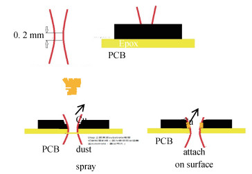
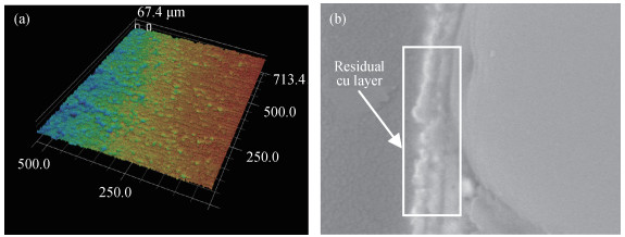
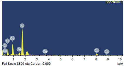
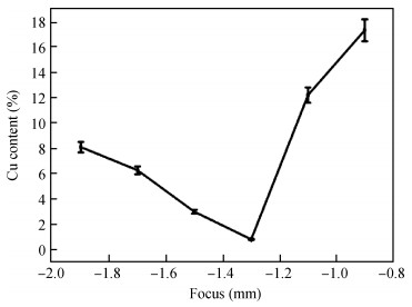
Table 1. Properties of compound.

|
| [1] |
Yu X J, Zhang X Y, Fan W, et al. Technology of electroles copper plating on ABS plastics. Electroplating & Finishing, 2007, 26(5): 10 http://en.cnki.com.cn/Article_en/CJFDTOTAL-DDTL200705004.htm
|
| [2] |
Domenech S C, Lima J E, Drago V, et al. Electroless plating of nickel-phosphorous on surface-modified poly (ethylene terephthalate) films. Appl Surf Sci, 2003, 220(1): 238 http://www.sciencedirect.com/science/article/pii/S0169433203008158
|
| [3] |
Van Eck W. Electromagnetic radiation from video display units: an eavesdropping risk. Computer & Security, 1985, (4): 269 http://www.sciencedirect.com/science/article/pii/016740488590046X
|
| [4] |
Laguarta F L. Laser application for optical glass polishing. Opt Soc Am, 1997, 56(24): 352 http://opticalengineering.spiedigitallibrary.org/article.aspx?articleid=1075148
|
| [5] |
Dai Y T, Xu G, Tong X L. Deep UV laser etching of GaN epilayers grown on sapphire substrate. J Mater Process Technol, 2012, 212(2): 492 doi: 10.1016/j.jmatprotec.2011.08.022
|
| [6] |
Shi E G, Zhao B. Modeling of chemical mechanical polishing with soft pads. Appl Phys A, 1998, 67: 249 doi: 10.1007/s003390050766
|
| [7] |
Hanh P O. The 300 mm silicon wafer-a cost and technology challenge. Microelectron Eng, 2001, 56(1/2): 3 https://www.researchgate.net/publication/223589930_The_300_mm_silicon_wafer_-_A_cost_and_technology_challenge
|
| [8] |
Steigerwald J M, Murka S P, Gutmann R J, et al. Chemical processes in the chemical mechanical polishing of copper. Mater Chem Phys, 1995, 41(3): 217 doi: 10.1016/0254-0584(95)01516-7
|
| [9] |
Yoshiki H, Hashimoto K, Fujishima A. Reaction mechanism of electroless metal deposition using ZnO thin film (Ⅰ): process of catalyst formation. Electrochem Soc, 1995, 142(2): 428 doi: 10.1149/1.2044049
|
| [10] |
Kretz F. The electroless deposition of nickel on SiC particles for aluminum matrix composites. Surf Coat Technol, 2004, 180/181: 575 doi: 10.1016/j.surfcoat.2003.10.150
|
| [11] |
Lindsay, Deborah J, Feldstein, et al. Activators for colloidal catalysts in electroless plating processes. US Patent, 4820547, 1988-06-27 http://www.freepatentsonline.com/4820547.html
|
| [12] |
Takino H, Shibata N, Itoh H, et al. Fabrication of optics by use of plasma chemical vaporization machining with a pipe electrode. Appl Opt, 2002, 41(19): 3971 doi: 10.1364/AO.41.003971
|
| [13] |
Bollinger D, Gallatin G, Samuels J, et al. Rapid, Noncontact optical figuring of aspheric surfaces with plasma assisted chemical etching (PACE) SPIE. Adv Opt Manufact Testing, 1990, 1333(23): 44 doi: 10.1117/12.22788
|
| [14] |
Zarowin C B. A comparison using surface evolution theory of the smoothing and figuring of optics by plasma assisted chemical etching and ion milling. SPIE, 1991(1618): 22 doi: 10.1117/12.58038
|
| [15] |
Solodlii E N, Solodkii N F. Reasond for tinting of corundum ceramics (a review). Glass and Ceramics, 2001, 58(11): 391 doi: 10.1023/A%3A1014910425932
|
| [16] |
Kacara E, Mutlua M, Akman E, et al. Characterization of the drilling alumina ceramic using Nd-YAG pulsed laser. J Mater Processing Technol, 2009, 209(4): 2008 doi: 10.1016/j.jmatprotec.2008.04.049
|
| [17] |
Hanon M M, Akman E, Genc O B, et al. Experimental and theoretical investigation of the drilling of alumina ceramic using Nd-YAG pulsed laser. Opt Laser Technol, 2012, 44(4): 913 doi: 10.1016/j.optlastec.2011.11.010
|
| [18] |
Brinksmeier E, Riemer O, Gessenharter A, et al. Polishing of structured molds. CIRP Annals-Manufact Technol, 2004, 53(1): 247 doi: 10.1016/S0007-8506(07)60690-8
|
| [19] |
Hua M, Shao T, Hong Y T, et al. Influence of pulse duration on the surface morphology of ASSAB DF-2(AISI-01) cold work steel treated by YAG laser. Surf Coat Technol, 2004, 185(2): 127 http://www.sciencedirect.com/science/article/pii/S0257897204000349
|
| [20] |
Trtica M, Gakovic B, Batani D, et al. Surface modifications of a titanium implant by a picosecond Nd: YAG laser operating at 1064 and 532 nm. Appl Surf Sci, 2006, 253(5): 2551 doi: 10.1016/j.apsusc.2006.05.024
|
| [21] |
Brusasco R M, Penetrante B M, Butler J A, et al. CO2 laser polishing for reduction of 351 nm surface damage initiation in fused silica. International Society for Optics and Photonics, 2002: 34 https://www.osti.gov/scitech/biblio/15004628-co2-laser-polishing-reduction-nm-surface-damage-initiation-fused-silica
|
| [22] |
Yang H, Huang S, Duan J, et al. Contrastive study on laser ablation of single-crystal silicon by 1030 nm femtosecond laser and 355 nm nanosecond laser. Chin J Lasers, 2013, 40(1): 0103003 doi: 10.3788/CJL
|


Article views: 4248 Times PDF downloads: 35 Times Cited by: 0 Times
Received: 11 October 2016 Revised: 15 November 2016 Online: Published: 01 May 2017
| Citation: |
Xinling Meng, Luqi Tao, Zhaolin Liu, Yi Yang, Tianling Ren. A novel polishing technology for epoxy resin based on 355 nm UV laser[J]. Journal of Semiconductors, 2017, 38(5): 056001. doi: 10.1088/1674-4926/38/5/056001
****
X L Meng, L Q Tao, Z L Liu, Y Yang, T L Ren. A novel polishing technology for epoxy resin based on 355 nm UV laser[J]. J. Semicond., 2017, 38(5): 056001. doi: 10.1088/1674-4926/38/5/056001.

|
| [1] |
Yu X J, Zhang X Y, Fan W, et al. Technology of electroles copper plating on ABS plastics. Electroplating & Finishing, 2007, 26(5): 10 http://en.cnki.com.cn/Article_en/CJFDTOTAL-DDTL200705004.htm
|
| [2] |
Domenech S C, Lima J E, Drago V, et al. Electroless plating of nickel-phosphorous on surface-modified poly (ethylene terephthalate) films. Appl Surf Sci, 2003, 220(1): 238 http://www.sciencedirect.com/science/article/pii/S0169433203008158
|
| [3] |
Van Eck W. Electromagnetic radiation from video display units: an eavesdropping risk. Computer & Security, 1985, (4): 269 http://www.sciencedirect.com/science/article/pii/016740488590046X
|
| [4] |
Laguarta F L. Laser application for optical glass polishing. Opt Soc Am, 1997, 56(24): 352 http://opticalengineering.spiedigitallibrary.org/article.aspx?articleid=1075148
|
| [5] |
Dai Y T, Xu G, Tong X L. Deep UV laser etching of GaN epilayers grown on sapphire substrate. J Mater Process Technol, 2012, 212(2): 492 doi: 10.1016/j.jmatprotec.2011.08.022
|
| [6] |
Shi E G, Zhao B. Modeling of chemical mechanical polishing with soft pads. Appl Phys A, 1998, 67: 249 doi: 10.1007/s003390050766
|
| [7] |
Hanh P O. The 300 mm silicon wafer-a cost and technology challenge. Microelectron Eng, 2001, 56(1/2): 3 https://www.researchgate.net/publication/223589930_The_300_mm_silicon_wafer_-_A_cost_and_technology_challenge
|
| [8] |
Steigerwald J M, Murka S P, Gutmann R J, et al. Chemical processes in the chemical mechanical polishing of copper. Mater Chem Phys, 1995, 41(3): 217 doi: 10.1016/0254-0584(95)01516-7
|
| [9] |
Yoshiki H, Hashimoto K, Fujishima A. Reaction mechanism of electroless metal deposition using ZnO thin film (Ⅰ): process of catalyst formation. Electrochem Soc, 1995, 142(2): 428 doi: 10.1149/1.2044049
|
| [10] |
Kretz F. The electroless deposition of nickel on SiC particles for aluminum matrix composites. Surf Coat Technol, 2004, 180/181: 575 doi: 10.1016/j.surfcoat.2003.10.150
|
| [11] |
Lindsay, Deborah J, Feldstein, et al. Activators for colloidal catalysts in electroless plating processes. US Patent, 4820547, 1988-06-27 http://www.freepatentsonline.com/4820547.html
|
| [12] |
Takino H, Shibata N, Itoh H, et al. Fabrication of optics by use of plasma chemical vaporization machining with a pipe electrode. Appl Opt, 2002, 41(19): 3971 doi: 10.1364/AO.41.003971
|
| [13] |
Bollinger D, Gallatin G, Samuels J, et al. Rapid, Noncontact optical figuring of aspheric surfaces with plasma assisted chemical etching (PACE) SPIE. Adv Opt Manufact Testing, 1990, 1333(23): 44 doi: 10.1117/12.22788
|
| [14] |
Zarowin C B. A comparison using surface evolution theory of the smoothing and figuring of optics by plasma assisted chemical etching and ion milling. SPIE, 1991(1618): 22 doi: 10.1117/12.58038
|
| [15] |
Solodlii E N, Solodkii N F. Reasond for tinting of corundum ceramics (a review). Glass and Ceramics, 2001, 58(11): 391 doi: 10.1023/A%3A1014910425932
|
| [16] |
Kacara E, Mutlua M, Akman E, et al. Characterization of the drilling alumina ceramic using Nd-YAG pulsed laser. J Mater Processing Technol, 2009, 209(4): 2008 doi: 10.1016/j.jmatprotec.2008.04.049
|
| [17] |
Hanon M M, Akman E, Genc O B, et al. Experimental and theoretical investigation of the drilling of alumina ceramic using Nd-YAG pulsed laser. Opt Laser Technol, 2012, 44(4): 913 doi: 10.1016/j.optlastec.2011.11.010
|
| [18] |
Brinksmeier E, Riemer O, Gessenharter A, et al. Polishing of structured molds. CIRP Annals-Manufact Technol, 2004, 53(1): 247 doi: 10.1016/S0007-8506(07)60690-8
|
| [19] |
Hua M, Shao T, Hong Y T, et al. Influence of pulse duration on the surface morphology of ASSAB DF-2(AISI-01) cold work steel treated by YAG laser. Surf Coat Technol, 2004, 185(2): 127 http://www.sciencedirect.com/science/article/pii/S0257897204000349
|
| [20] |
Trtica M, Gakovic B, Batani D, et al. Surface modifications of a titanium implant by a picosecond Nd: YAG laser operating at 1064 and 532 nm. Appl Surf Sci, 2006, 253(5): 2551 doi: 10.1016/j.apsusc.2006.05.024
|
| [21] |
Brusasco R M, Penetrante B M, Butler J A, et al. CO2 laser polishing for reduction of 351 nm surface damage initiation in fused silica. International Society for Optics and Photonics, 2002: 34 https://www.osti.gov/scitech/biblio/15004628-co2-laser-polishing-reduction-nm-surface-damage-initiation-fused-silica
|
| [22] |
Yang H, Huang S, Duan J, et al. Contrastive study on laser ablation of single-crystal silicon by 1030 nm femtosecond laser and 355 nm nanosecond laser. Chin J Lasers, 2013, 40(1): 0103003 doi: 10.3788/CJL
|

 WeChat ID
Journal of Semiconductors © 2017 All Rights Reserved 京ICP备05085259号-2

 DownLoad:

