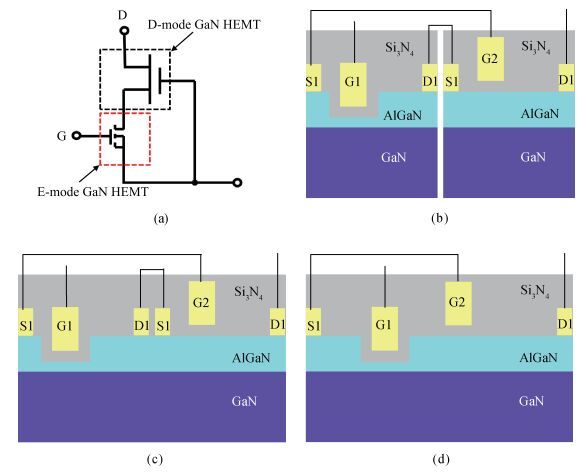
Processing math: 100%
J. Semicond. > 2017, Volume 38 > Issue 7 > 074001

SEMICONDUCTOR DEVICES

Design and simulation of a novel E-mode GaN MIS-HEMT based on a cascode connection for suppression of electric field under gate and improvement of reliability

Weiyi Li1, 2, #, Zhili Zhang1, 2, #, Kai Fu1, Guohao Yu1, Xiaodong Zhang1, Shichuang Sun1, 3, Liang Song1, 2, Ronghui Hao1, 4, Yaming Fan1, Yong Cai1 and Baoshun Zhang1, 5,

+ Author Affiliations

 Corresponding author: Baoshun Zhang,Email: bszhang2006@sinano.ac.cn

DOI: 10.1088/1674-4926/38/7/074001

PDF

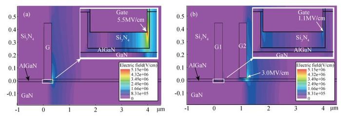
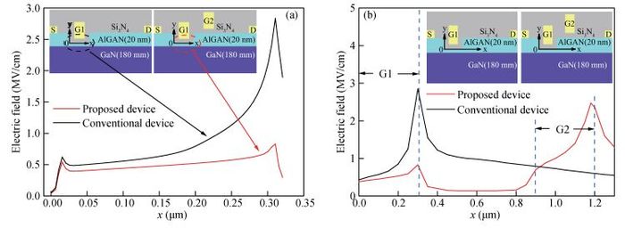
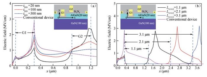
Abstract: We proposed a novel AlGaN/GaN enhancement-mode (E-mode) high electron mobility transistor (HEMT) with a dual-gate structure and carried out the detailed numerical simulation of device operation using Silvaco Atlas. The dual-gate device is based on a cascode connection of an E-mode and a D-mode gate. The simulation results show that electric field under the gate is decreased by more than 70% compared to that of the conventional E-mode MIS-HEMTs (from 2.83 MV/cm decreased to 0.83 MV/cm). Thus, with the discussion of ionized trap density, the proposed dual-gate structure can highly improve electric field-related reliability, such as, threshold voltage stability. In addition, compared with HEMT with field plate structure, the proposed structure exhibits a simplified fabrication process and a more effective suppression of high electric field.

Key words: GaN HEMTenhancement-modeelectric field distributionVth instability

As a promising candidate for the next-generation power electronic device, AlGaN/GaN HEMT shows strong potential for high-power and high-frequency applications with its unique properties [1-3]. The conventional GaN HEMT is a depletion mode device and an enhancement mode device is highly desirable in the application due to the fail-safe operation and its simplified circuit design. Several approaches have been proposed to realize the E-mode GaN HEMT, such as gate recess [4-6], fluorine ion implantation [7-9], p-GaN cap [10] etc. Among them, the gate recess and fluorine ion implantation MIS-HEMTs are considered as promising candidates because they allow low gate leakage current as well as large gate swing. However, it still remains challenging to obtain stable E-mode MIS-HEMT. For gate recess structure, the high-density traps with short and long emission time constants τit at the dielectric/(Al)GaN interface were caused by gate recessing, and the dynamic charging/discharging processes of these interface states' traps can lead to the threshold voltage instability issue when a high off-state VDS stress is applied to the device [11]. For fluorine ion implantation MIS-HEMT, one important issue to address is the stability and reliability of the fluorine ions, and consequently the threshold voltage stability during the device operation, especially under high electric-field electrical stress or high temperature stress application [11, 12].

In this study, a novel dual-gate E-mode MIS-HEMT device that is based on a cascode connection of an E-mode and a D-mode gate is proposed and analyzed using Atlas simulation toolbox by Silvaco. The on-state as well as off-state electrical performances are investigated. In comparison with that of conventional E-mode HEMT, the electric field concentration under the E-mode HEMT gate is effectively suppressed, which is transferred to the area under the D-mode HEMT gate during the off-state stress period. Thus, the proposed dual-gate structure can highly improve the electric field under the gate-related reliability, such as, threshold voltage stability. In order to better understand the dynamic charging/discharging processes, a specific example of acceptor-like traps is introduced at the interface of AlGaN/Si 3 N 4 to simulate and discuss the interface states trap-induced Vth instability issue. The results show that the proposed structure can effectively decrease variation of ionized traps, and consequently improve the threshold voltage's stability.

Fig. 1(a) illustrates the equivalent circuit of the proposed novel E-mode MISHEMT. Implementations of the device are illustrated in Figs. 1(b)-1(d). The hybrid E-mode MISHEMT presented in Fig. 1(b) is formed of an E-mode and a D-mode MISHEMT. The source electrode of the E-mode and the gate electrode of the D-mode MISHEMT are electrically connected. The source electrode of the D-mode MISHEMT is electrically connected to the drain electrode of the E-mode MISHEMT, leading to the conductive current being controlled by the gate of E-mode MISHEMT. Compared to the device of Fig. 1(b), the stack configuration shown in Fig. 1(c) has lower parasitic inductance and can also reduce the cost of fabrication and packaging. Moreover, considering that the contacts that form the drain of E-mode and the source of D-mode MISHEMT are not used for any functional purpose during device operation, these contacts are omitted in Fig. 1(d), showing the proposed E-mode MISHEMT structure.

Figure  1.  (a) Equivalent circuit of the proposed novel enhancement-mode GaN HEMT and (b)(c)(d) implementations of the proposed device.

The schematics cross-section and key parameters of the optimized novel E-mode MIS-HEMT and conventional gate recessed MIS-HEMT are shown in Figs. 2(a) and 2(b) respectively. The proposed dual-gate structure consists of a 20 nm Al 0.2 Ga 0.8 N barrier layer, a 180 nm GaN buffer layer and a Si 3 N 4 passivation layer on the top. The lengths of the E-mode and D-mode gates are 300 nm. The source-to-gate and drain-to-gate spaces are 1 μ m ( LGS=1 μ m) and 4.2 μ m ( LGD=4.2 μ m), respectively. It features a distance between two gates of 600 nm ( LG1G2=600 nm). To achieve the positive threshold voltage, a recess depth of 18 nm with 2 nm AlGaN left is performed under the gate. The gate dielectric for both gates is set to be 8 nm Si 3 N 4 . The conventional gate recess structure shares all structural parameters with the proposed E-mode MIS-HEMT, except for the existence of the D-mode gate.

The Shockley-Read-Hall recombination model [13, 14] and the Caughey and Thomas field-dependent mobility model [15] are included in all simulations. Material parameters of GaN and AlN used in the Atlas simulations and calculated in Poisson's equation, continuity equations for electrons and holes, and transport equations using the drift-diffusion model are extracted from Ref. [16]. The spontaneous and piezoelectric polarizations of the wurtzite polarization model are taken into account using the built-in self-consistent polarization model of the Atlas toolbox by Silvaco [17]. To model the mechanism of traps, electrons that are emitted or captured are considered to maintain charge self-consistency, modifying the recombination rate in the carrier continuity equations of Shockley-Read-Hall recombination model [18].

Figure  2.  Schematic cross-section of the (a) conventional E-mode HEMT with gate recess and (b) proposed novel E-mode HEMT.

Fig. 3 shows the comparisons of DC characteristics of the conventional gate recess device and proposed E-mode device. The threshold voltages of 0.3 V for both devices were obtained by linear extraction The maximum Gm values are 325 mS/mm at VGS=24 V and 321 mS/mm at VGS=22 V for conventional gate recess device and proposed E-mode device respectively The conventional gate recess device exhibits a maximum drain current of 860 mA/mm while the proposed device's maximum drain current is 793 mA/mm at VGS=10 V and VDS=5 V, as shown in Fig. 3(a); the slight difference (67 mA/mm) can be explained with the Schottky barrier altitude of the D-mode gate contact. The output characteristics of two devices are shown in Fig. 3(b). The on-state resistance of 4.06 Ω cm 2 and 4.78 Ω cm 2 are both obtained at VGS=5 V for conventional device and proposed device, respectively. All these results show almost no degradation compared with that observed in the conventional E-mode MIS-HEMT, except a slight decrease on maximum drain current due to the introduction of the D-mode gate.

Figure  3.  Comparisons of DC characteristics of these two devices with (a) transfer characteristics and (b) outputs characteristics.

Considering no obvious degradation is observed in basic electrical performance, the off-state characteristic is investigated. Fig. 4 presents the distribution of off-state electric field at VDS=100 V and VGS=0 V for both structures. The electric field concentration under the gate is effectively suppressed for the proposed device. The highest electric field intensity of the entire device (5.5 MV/cm) locates underneath the drain edge of the gate for conventional structure, and it is transferred to the edge of D-mode gate in the proposed structure with a value of 3.0 MV/cm. As shown in Fig. 5(a), the maximum electric field at Si 3 N 4 /AlGaN interface under the gate are 2.83 MV/cm and 0.83 MV/cm for conventional gate recess device and proposed E-mode device, respectively. Fig. 5(b) gives the distributions of electric field at Si 3 N 4 /AlGaN interface for both structures, and it is obvious that the peak electric field (2.83 MV/cm) at the gate edge is weakened to 2.49 MV/cm and moved to the area under the D-mode gate during the off-state stress period. It should be noted that the recess gate determining the device's Vth of the proposed device is shielded from the high electric field, even under high drain voltage.

Figure  4.  Schematic cross-section of electric field distribution of (a) conventional structure and (b) proposed structure at VDS=100 V and VGS=0 V.
Figure  5.  (a) Electric field distribution under gates for both structures at VDS=100 V and VGS=0 V and (b) maximum electric field distribution near the gates for both structures.

For verification and to better understand the suppression effect for the electric field under gate, more simulation and discussion are performed. Considering Si 3 N 4 thickness under the D-mode gate and distance between two gates are two important design parameters, relative simulations are carried out and analyzed. The electric field distribution at Si 3 N 4 /AlGaN interface as a function of the Si 3 N 4 thickness is simulated and given in Fig. 6(a) The peak electric field under E-mode gate of 1.15, 1.70, and 1.91 MV/cm was extracted from Si 3 N 4 thickness of 20, 100, and 300 nm, respectively. The electric field at edge of the D-mode gate is decreased from 2.41 to 1.54 MV/cm and continues to fall to 1.06 MV/cm For comparison, the electric field intensities are 2.85 and 0.62 MV/cm at the corresponding area for conventional gate recess device. According to this result suppression effect for the electric field is discovered with different Si 3 N 4 thickness, but there is a tradeoff between these two electric field distributions. With the increase of the Si 3 N 4 film thickness, the electric field under E-mode gate increases whereas electric field concentration under the D-mode gate is reduced. When the Si 3 N 4 thickness reaches to 300 nm or more than 300 nm, the suppression effect is similar to the device with source field plate, and more detailed discussion will be conducted in Section 2.6.

Figure  6.  (a) Relationship between the electric field distribution and the Si 3 N 4 thickness under the D-mode gate and (b) Electric field distribution with different distance between two gates at VDS=100 V and VGS=0 V.

Fig. 6(b) presents the relationship between the distance between two gates and electric field distribution. Distinguishable electric field transfer effect is found with the variety of LG1G2 , and the electric field concentration moved to the edge of the D-mode gate along with the change of distance between two gates. Moreover, good suppression effects for electric field under the E-mode gates are achieved for all structures (less than 0.82 MV/cm). Therefore, the proposed structure is believed to transfer the electric field concentration at the gate edge and have an effective suppression effect for the electric field under the gate.

It has been proven that the charging/discharging behavior of dielectric/(Al)GaN interface states is related to the electric field intensity at the interface [19]. In order to better understand this process, a specific example of acceptor-like traps is introduced at the interface of Si 3 N 4 /AlGaN to measure the interface states-induced Vth shift, the acceptor level is set at 0.35 eV below the conduction band, and the density is fixed at a typical value of 1 × 10 13 cm 2 based on the work of Refs. [19, 20]. The Si 3 N 4 thickness under the D-mode gate and distance between two gates are set to be 8 and 600 nm for consistence and convergence. Both of the structures are first biased with VGS=0 V and VDS=0 V for original state, then voltage stress with VDS=100 V and VGS=0 V is applied to devices for 1 ms, finally returning to the original state. Besides, a longer stress time of 10 ms is performed to verify the effectiveness of the proposed structure on a longer timescale.

Fig. 7 shows the distribution of the ionized traps for both structures at original state, after the 1 ms off-state stress and after the 10 ms off-state stress. It is clearly observed that the variation of ionized traps' density before and after the off-state stress is effectively decreased in the proposed structure due to its suppression of the electric field under the gate. As shown in Fig. 8(a), for conventional E-mode HEMT, the densities of ionized traps at the gate edge ( x=0.3 μ m) are 1 × 10 13 , 8 × 10 5 and 2 cm 2 for original state, after the 1 ms off-state stress and after the 10 ms off-state stress, respectively, meanwhile the ionized state density shows an overall decrease for the entire space under the gate. It is believed that the variation of ionized traps' density accounts for the change of the charge density under the gate, which causes Vth instability [21]. For comparison, Fig. 8(b) gives the density of the ionized traps under the gate of the proposed structure for three states. A slight difference was observed before and after off-state stress, suggesting that the proposed structure is effective for suppressing the variation of ionized traps density. So the proposed structure can prevent the shift in Vth and improve reliability by shielding the gate with D-mode gate from high electric-field.

Figure  7.  Distribution of the ionized traps of both structures at (a) original condition at VGS=0 V and VDS=0 V and (b) after the 1 ms off-state stress and (c) after the 10 ms off-state stress.
Figure  8.  Ionized traps' density for the AlGaN/Si 3 N 4 interface under gates of (a) conventional structure and (b) proposed dual-gate structure.

To better understand the difference between the device with source field plate and the proposed dual-gate device, the simulation of the device with source field plate was performed. Fig. 9(a) shows the schematic cross-section of conventional gate recess device with source field plate, which shares the same structural parameters and the introduction of acceptor-like traps of conventional gate recess device except for the source field plate. The thickness of Si 3 N 4 under the field plate is 400 nm, based on Ref. [22]. The source field plate extension at the drain 2.2 μ m. Other parameters and simulation settings are the same as that of the proposed structure.

Figure  9.  (a) Schematic cross-section of conventional gate recess device with source field plate and (b) Electric field distribution and density of ionized traps under the gate for the device with source field plate.

Fig. 9(b) presents simulated electric field distribution and density of ionized traps under the gate of conventional gate recess device with source field plate, showing a good agreement with expected modulation effect on the electric field of the source field plate [22]. However, an electric field peak of 1.95 MV/cm at the edge of the gate and an obvious decrease in the density of ionized traps are observed. After comparison with the proposed structure, the proposed novel E-mode MIS-HEMT exhibits a more effective suppression of electric field under the gate and a simplified fabrication process with a single step of gate metal photolithography.

A novel AlGaN/GaN E-mode HEMT with a dual-gate structure was proposed and simulated by Silvaco Atlas. The dual-gate device is based on a cascode connection of an E-mode and a D-mode gate. The electric field under the gate is effectively suppressed, which is transferred to the area under the D-mode HEMT gate during the off-state stress period. As a result, the proposed structure can effectively decrease variation of ionized traps, and consequently improve the threshold voltage's stability by shielding the E-mode gate with a D-mode gate from high electric field.

Acknowledgments: We thank the Suzhou nanofabrication facility of SINANO, CAS, for the fabrication, characterization and testing of the AlGaN/GaN MIS-HEMT.


[1]
Karmalkar S, Mishra U K. Enhancement of breakdown voltage in AlGaN/GaN high electron mobility transistors using a field plate. IEEE Trans Electron Devices, 2001, 48: 1515 doi: 10.1109/16.936500
[2]
Dong Z, Hao R, Zhang Z, et al. Impact of N-plasma treatment on the current collapse of ALGAN/GAN HEMTs. 12th IEEE International Conference on Solid-State and Integrated Circuit Technology (ICSICT), 2014: 1 http://ieeexplore.ieee.org/abstract/document/7021380
[3]
Wang Z, Zhou J, Kong Y, et al. Thin-barrier enhancement-mode AlGaN/GaN MIS-HEMT using ALD Al2O3 as gate insulator. J Semicond, 2015, 36: 094004 doi: 10.1088/1674-4926/36/9/094004
[4]
Saito W, Takada Y, Kuraguchi M, et al. Recessed-gate structure approach toward normally off high-voltage AlGaN/GaN HEMT for power electronics applications. IEEE Trans Electron Devices, 2006, 53: 356 doi: 10.1109/TED.2005.862708
[5]
Xu Z, Wang J, Cai Y, et al. Enhancement mode (E-mode) AlGaN/GaN MOSFET with A/mm leakage current and ON/OFF current ratio. IEEE Electron Device Lett, 2014, 35: 1200 doi: 10.1109/LED.2014.2360541
[6]
Wang Y, Wang M, Xie B, et al. High-performance normally-off MOSFET using a wet etching-based gate recess technique. IEEE Electron Device Lett, 2013, 34: 1370 doi: 10.1109/LED.2013.2279844
[7]
Cai Y, Zhou Y, Lau K M, et al. Control of threshold voltage of AlGaN/GaN HEMTs by fluoride-based plasma treatment: from depletion mode to enhancement mode. IEEE Trans Electron Devices, 2006, 53: 2207 doi: 10.1109/TED.2006.881054
[8]
Zhang Z, Fu K, Deng X, et al. Normally off AlGaN/GaN MIS-high-electron mobility transistors fabricated by using low pressure chemical vapor deposition Si3N4 gate dielectric and standard fluorine ion implantation. IEEE Electron Device Lett, 2015, 36: 1128 doi: 10.1109/LED.2015.2483760
[9]
Chen Y, Zheng X, Zhang J, et al. Monolithically integrated enhancement/depletion-mode AlGaN/GaN HEMTs SRAM unit and voltage level shifter using fluorine plasma treatment. J Semicond, 2016, 37: 055002 doi: 10.1088/1674-4926/37/5/055002
[10]
Uemoto Y, Hikita M, Ueno V, et al. Gate injection transistor (GIT)-a normally-off AlGaN/GaN power transistor using conductivity modulation. IEEE Trans Electron Devices, 2007, 54: 3393 doi: 10.1109/TED.2007.908601
[11]
Meneghesso G, Meneghini M, Zanoni E. Reliability and instabilities in GaN-based HEMTs. IEEE International Conference on Electron Devices and Solid-State Circuits (EDSSC), 2014: 1 http://ieeexplore.ieee.org/document/7061275/
[12]
Yi C, Wang R, Huang W, et al. Reliability of enhancement-mode AlGaN/GaN HEMTs fabricated by fluorine plasma treatment. 2007 IEEE International Electron Devices Meeting, 2007: 389 http://ieeexplore.ieee.org/document/4418954/?reload=true&arnumber=4418954&sortType%3Dasc_p_Sequence%26filter%3DAND%28p_IS_Number%3A4418848%29%26pageNumber%3D2%26rowsPerPage%3D100
[13]
Shockley W, Read W Jr. Statistics of the recombinations of holes and electrons. Phys Rev, 1952, 87: 835 doi: 10.1103/PhysRev.87.835
[14]
Hall R N. Electron--hole recombination in germanium. Phys Rev, 1952, 87: 387 doi: 10.1103/PhysRev.87.387
[15]
Caughey D M, Thomas R E. Carrier mobilities in silicon empirically related to doping and field. Proc IEEE, 1967, 55: 2192 doi: 10.1109/PROC.1967.6123
[16]
Piprek J. Semiconductor optoelectronic devices: introduction to physics and simulation. Academic Press, 2013
[17]
Ambacher O, Foutz B, Smart J, et al. Two dimensional electron gases induced by spontaneous and piezoelectric polarization in undoped and doped AlGaN/GaN heterostructures. J Appl Phys, 2000, 87: 334 doi: 10.1063/1.371866
[18]
Simmons J, Taylor G. Nonequilibrium steady-state statistics and associated effects for insulators and semiconductors containing an arbitrary distribution of traps. Phys Rev B, 1971, 4: 502 doi: 10.1103/PhysRevB.4.502
[19]
Wu T L, Marcon D, Bakeroot B, et al. Correlation of interface states/border traps and threshold voltage shift on AlGaN/GaN metal-insulator-semiconductor high-electron-mobility transistors. Appl Phys Lett, 2015, 107: 4 https://biblio.ugent.be/publication/6972789/file/6972802.pdf
[20]
Zhang Z, Yu G, Zhang X, et al. Studies on high-voltage GaN-on-Si MIS-HEMTs using LPCVD Si3N4 as gate dielectric and passivation layer. IEEE Trans Electron Devices, 2016, 63: 731 doi: 10.1109/TED.2015.2510445
[21]
Meneghini M, Rossetto I, Bisi D, et al. Negative bias-induced threshold voltage instability in GaN-on-Si power HEMTs. IEEE Electron Device Lett, 2016, 37: 474 doi: 10.1109/LED.2016.2530693
[22]
Saito W, Kuraguchi M, Takada Y, et al. Design optimization of high breakdown voltage AlGaN-GaN power HEMT on an insulating substrate for RONAVB tradeoff characteristics. IEEE Trans Electron Devices, 2005, 52: 106 doi: 10.1109/TED.2004.841338
Fig. 1.  (a) Equivalent circuit of the proposed novel enhancement-mode GaN HEMT and (b)(c)(d) implementations of the proposed device.

Fig. 2.  Schematic cross-section of the (a) conventional E-mode HEMT with gate recess and (b) proposed novel E-mode HEMT.

Fig. 3.  Comparisons of DC characteristics of these two devices with (a) transfer characteristics and (b) outputs characteristics.

Fig. 4.  Schematic cross-section of electric field distribution of (a) conventional structure and (b) proposed structure at VDS=100 V and VGS=0 V.

Fig. 5.  (a) Electric field distribution under gates for both structures at VDS=100 V and VGS=0 V and (b) maximum electric field distribution near the gates for both structures.

Fig. 6.  (a) Relationship between the electric field distribution and the Si 3 N 4 thickness under the D-mode gate and (b) Electric field distribution with different distance between two gates at VDS=100 V and VGS=0 V.

Fig. 7.  Distribution of the ionized traps of both structures at (a) original condition at VGS=0 V and VDS=0 V and (b) after the 1 ms off-state stress and (c) after the 10 ms off-state stress.

Fig. 8.  Ionized traps' density for the AlGaN/Si 3 N 4 interface under gates of (a) conventional structure and (b) proposed dual-gate structure.

Fig. 9.  (a) Schematic cross-section of conventional gate recess device with source field plate and (b) Electric field distribution and density of ionized traps under the gate for the device with source field plate.

[1]
Karmalkar S, Mishra U K. Enhancement of breakdown voltage in AlGaN/GaN high electron mobility transistors using a field plate. IEEE Trans Electron Devices, 2001, 48: 1515 doi: 10.1109/16.936500
[2]
Dong Z, Hao R, Zhang Z, et al. Impact of N-plasma treatment on the current collapse of ALGAN/GAN HEMTs. 12th IEEE International Conference on Solid-State and Integrated Circuit Technology (ICSICT), 2014: 1 http://ieeexplore.ieee.org/abstract/document/7021380
[3]
Wang Z, Zhou J, Kong Y, et al. Thin-barrier enhancement-mode AlGaN/GaN MIS-HEMT using ALD Al2O3 as gate insulator. J Semicond, 2015, 36: 094004 doi: 10.1088/1674-4926/36/9/094004
[4]
Saito W, Takada Y, Kuraguchi M, et al. Recessed-gate structure approach toward normally off high-voltage AlGaN/GaN HEMT for power electronics applications. IEEE Trans Electron Devices, 2006, 53: 356 doi: 10.1109/TED.2005.862708
[5]
Xu Z, Wang J, Cai Y, et al. Enhancement mode (E-mode) AlGaN/GaN MOSFET with A/mm leakage current and ON/OFF current ratio. IEEE Electron Device Lett, 2014, 35: 1200 doi: 10.1109/LED.2014.2360541
[6]
Wang Y, Wang M, Xie B, et al. High-performance normally-off MOSFET using a wet etching-based gate recess technique. IEEE Electron Device Lett, 2013, 34: 1370 doi: 10.1109/LED.2013.2279844
[7]
Cai Y, Zhou Y, Lau K M, et al. Control of threshold voltage of AlGaN/GaN HEMTs by fluoride-based plasma treatment: from depletion mode to enhancement mode. IEEE Trans Electron Devices, 2006, 53: 2207 doi: 10.1109/TED.2006.881054
[8]
Zhang Z, Fu K, Deng X, et al. Normally off AlGaN/GaN MIS-high-electron mobility transistors fabricated by using low pressure chemical vapor deposition Si3N4 gate dielectric and standard fluorine ion implantation. IEEE Electron Device Lett, 2015, 36: 1128 doi: 10.1109/LED.2015.2483760
[9]
Chen Y, Zheng X, Zhang J, et al. Monolithically integrated enhancement/depletion-mode AlGaN/GaN HEMTs SRAM unit and voltage level shifter using fluorine plasma treatment. J Semicond, 2016, 37: 055002 doi: 10.1088/1674-4926/37/5/055002
[10]
Uemoto Y, Hikita M, Ueno V, et al. Gate injection transistor (GIT)-a normally-off AlGaN/GaN power transistor using conductivity modulation. IEEE Trans Electron Devices, 2007, 54: 3393 doi: 10.1109/TED.2007.908601
[11]
Meneghesso G, Meneghini M, Zanoni E. Reliability and instabilities in GaN-based HEMTs. IEEE International Conference on Electron Devices and Solid-State Circuits (EDSSC), 2014: 1 http://ieeexplore.ieee.org/document/7061275/
[12]
Yi C, Wang R, Huang W, et al. Reliability of enhancement-mode AlGaN/GaN HEMTs fabricated by fluorine plasma treatment. 2007 IEEE International Electron Devices Meeting, 2007: 389 http://ieeexplore.ieee.org/document/4418954/?reload=true&arnumber=4418954&sortType%3Dasc_p_Sequence%26filter%3DAND%28p_IS_Number%3A4418848%29%26pageNumber%3D2%26rowsPerPage%3D100
[13]
Shockley W, Read W Jr. Statistics of the recombinations of holes and electrons. Phys Rev, 1952, 87: 835 doi: 10.1103/PhysRev.87.835
[14]
Hall R N. Electron--hole recombination in germanium. Phys Rev, 1952, 87: 387 doi: 10.1103/PhysRev.87.387
[15]
Caughey D M, Thomas R E. Carrier mobilities in silicon empirically related to doping and field. Proc IEEE, 1967, 55: 2192 doi: 10.1109/PROC.1967.6123
[16]
Piprek J. Semiconductor optoelectronic devices: introduction to physics and simulation. Academic Press, 2013
[17]
Ambacher O, Foutz B, Smart J, et al. Two dimensional electron gases induced by spontaneous and piezoelectric polarization in undoped and doped AlGaN/GaN heterostructures. J Appl Phys, 2000, 87: 334 doi: 10.1063/1.371866
[18]
Simmons J, Taylor G. Nonequilibrium steady-state statistics and associated effects for insulators and semiconductors containing an arbitrary distribution of traps. Phys Rev B, 1971, 4: 502 doi: 10.1103/PhysRevB.4.502
[19]
Wu T L, Marcon D, Bakeroot B, et al. Correlation of interface states/border traps and threshold voltage shift on AlGaN/GaN metal-insulator-semiconductor high-electron-mobility transistors. Appl Phys Lett, 2015, 107: 4 https://biblio.ugent.be/publication/6972789/file/6972802.pdf
[20]
Zhang Z, Yu G, Zhang X, et al. Studies on high-voltage GaN-on-Si MIS-HEMTs using LPCVD Si3N4 as gate dielectric and passivation layer. IEEE Trans Electron Devices, 2016, 63: 731 doi: 10.1109/TED.2015.2510445
[21]
Meneghini M, Rossetto I, Bisi D, et al. Negative bias-induced threshold voltage instability in GaN-on-Si power HEMTs. IEEE Electron Device Lett, 2016, 37: 474 doi: 10.1109/LED.2016.2530693
[22]
Saito W, Kuraguchi M, Takada Y, et al. Design optimization of high breakdown voltage AlGaN-GaN power HEMT on an insulating substrate for RONAVB tradeoff characteristics. IEEE Trans Electron Devices, 2005, 52: 106 doi: 10.1109/TED.2004.841338
1

High threshold voltage enhancement-mode GaN p-FET with Si-rich LPCVD SiNx gate insulator for high hole mobility

Liyang Zhu, Kuangli Chen, Ying Ma, Yong Cai, Chunhua Zhou, et al.

Journal of Semiconductors, 2023, 44(8): 082801. doi: 10.1088/1674-4926/44/8/082801

2

High-performance enhancement-mode GaN-based p-FETs fabricated with O3-Al2O3/HfO2-stacked gate dielectric

Hao Jin, Sen Huang, Qimeng Jiang, Yingjie Wang, Jie Fan, et al.

Journal of Semiconductors, 2023, 44(10): 102801. doi: 10.1088/1674-4926/44/10/102801

3

Instability of parasitic capacitance in T-shape-gate enhancement-mode AlGaN/GaN MIS-HEMTs

Lan Bi, Yixu Yao, Qimeng Jiang, Sen Huang, Xinhua Wang, et al.

Journal of Semiconductors, 2022, 43(3): 032801. doi: 10.1088/1674-4926/43/3/032801

4

Static characteristics and short channel effect in enhancement-mode AlN/GaN/AlN N-polar MISFET with self-aligned source/drain regions

Bin Li, Lan Wei, Cai Wen

Journal of Semiconductors, 2014, 35(12): 124006. doi: 10.1088/1674-4926/35/12/124006

5

The influence of the channel electric field distribution on the polarization Coulomb field scattering in AlN/GaN heterostructure field-effect transistors

Yingxia Yu, Zhaojun Lin, Yuanjie Lü, Zhihong Feng, Chongbiao Luan, et al.

Journal of Semiconductors, 2014, 35(12): 124007. doi: 10.1088/1674-4926/35/12/124007

6

DC and RF characteristics of enhancement-mode InAlN/GaN HEMT with fluorine treatment

Xubo Song, Guodong Gu, Shaobo Dun, Yuanjie Lü, Tingting Han, et al.

Journal of Semiconductors, 2014, 35(4): 044002. doi: 10.1088/1674-4926/35/4/044002

7

Enhancement-mode InAlN/GaN MISHEMT with low gate leakage current

Gu Guodong, Cai Yong, Feng Zhihong, Liu Bo, Zeng Chunhong, et al.

Journal of Semiconductors, 2012, 33(6): 064004. doi: 10.1088/1674-4926/33/6/064004

8

A high-performance enhancement-mode AlGaN/GaN HEMT

Feng Zhihong, Xie Shengyin, Zhou Rui, Yin Jiayun, Zhou Wei, et al.

Journal of Semiconductors, 2010, 31(8): 084001. doi: 10.1088/1674-4926/31/8/084001

9

Enhancement-mode AlGaN/GaN HEMTs fabricated by fluorine plasma treatment

Quan Si, Hao Yue, Ma Xiaohua, Xie Yuanbin, Ma Jigang, et al.

Journal of Semiconductors, 2009, 30(12): 124002. doi: 10.1088/1674-4926/30/12/124002

10

Noise performance in AlGaN/GaN HEMTs under high drain bias

Pang Lei, Pu Yan, Liu Xinyu, Wang Liang, Liu Jian, et al.

Journal of Semiconductors, 2009, 30(8): 084004. doi: 10.1088/1674-4926/30/8/084004

11

Annealing before gate metal deposition related noise performance in AlGaN/GaN HEMTs

Pang Lei, Pu Yan, Liu Xinyu, Wang Liang, Li Chengzhan, et al.

Journal of Semiconductors, 2009, 30(5): 054001. doi: 10.1088/1674-4926/30/5/054001

12

Gate Annealing of an Enhancement-Mode InGaP/AlGaAs/InGaAs PHEMT

Li Ming, Zhang Haiying, Xu Jingbo, Li Xiao, Liu Liang, et al.

Journal of Semiconductors, 2008, 29(8): 1487-1490.

13

X-Band Internally-Matched GaN HEMTs

Wang Yong, Li Jingqiang, Zhang Zhiguo, Feng Zhen, Song Jianbo, et al.

Journal of Semiconductors, 2008, 29(9): 1783-1785.

14

A 5.1W/mm Power Density GaN HEMT on Si Substrate

Feng Zhihong, Yin Jiayun, Yuan Fengpo, Liu Bo, Liang Dong, et al.

Chinese Journal of Semiconductors , 2007, 28(12): 1949-1951.

15

Abstraction of Small Signal Equivalent Circuit Parameters of Enhancement-Mode InGaP/AlGaAs/InGaAs PHEMT

Xu Jingbo, Yin Junjian, Zhang Haiying, Li Xiao, Liu Liang, et al.

Chinese Journal of Semiconductors , 2007, 28(3): 361-364.

16

A 22-Element Small-Signal Model of GaN HEMT Devices

Liu Dan, Chen Xiaojuan, Liu Xinyu, Wu Dexin

Chinese Journal of Semiconductors , 2007, 28(9): 1438-1442.

17

A New Small-Signal Modeling and Extraction Method in AlGaN/GaN HEMTs

Lu Jing, Wang Yan, Ma Long, Yu Zhiping

Chinese Journal of Semiconductors , 2007, 28(4): 567-572.

18

An Analytical Model for the Surface Electrical Field Distribution and Optimization of Bulk-Silicon Double RESURF Devices

Li Qi, Li Zhaoji, Zhang Bo

Chinese Journal of Semiconductors , 2006, 27(7): 1177-1182.

19

A Research on Current Collapse of GaN HEMTs Under DC High Voltage

Long Fei, Du Jiangfeng, Luo Qian, Zhou Wei, Xia Jianxin, et al.

Chinese Journal of Semiconductors , 2006, 27(S1): 227-230.

20

Monolithic Integration of InGaP/AlGaAs/InGaAs Enhancement/Depletion-Mode PHEMTs

Li Haiou, Zhang Haiying, Yin Junjian, Ye Tianchun

Chinese Journal of Semiconductors , 2005, 26(12): 2281-2285.

1. Wang, Z., Sun, X., Ren, B. et al. Resonant driving scheme for p-doped gallium nitride high electron mobility transistor to reduce driving power loss. Energy Reports, 2023. doi:10.1016/j.egyr.2023.05.191
2. Lin, D.-J., Chang, C.-K., Barman, K. et al. Normally-Off AlGaN/GaN HEMTs With a Low Reverse Conduction Turn-On Voltage. IEEE Access, 2023. doi:10.1109/ACCESS.2023.3312726
3. Liu, X., Chiu, H.-C., Liu, C.-H. et al. Normally-off p-GaN Gated AlGaN/GaN HEMTs Using Plasma Oxidation Technique in Access Region. IEEE Journal of the Electron Devices Society, 2020. doi:10.1109/JEDS.2020.2975620
4. Liu, C.-H., Chiu, H.-C., Huang, C.-R. et al. Low gate lag normally-off p-GaN/AlGaN/GaN high electron mobility transistor with zirconium gate metal. Crystals, 2020, 10(1): 25. doi:10.3390/cryst10010025
5. Liu, C.-H., Kao, H.-L., Chiu, H.-C. et al. Improved dynamic ON-resistance of a normally off p-GaN gate high-electron-mobility transistor using a nongated-region oxidation technique. 2019.
6. Singh, P., Kumari, V., Saxena, M. et al. Threshold Voltage Investigation of Recessed Dual-Gate MISHEMT: Simulation Study. Communications in Computer and Information Science, 2019. doi:10.1007/978-981-13-5950-7_33
7. Tang, W.-X., Hao, R.-H., Chen, F. et al. p-GaN hybrid anode AlGaN/GaN diode with 1000 V operation | [1000 V p-GaN混合阳极AlGaN/GaN二极管]. Wuli Xuebao/Acta Physica Sinica, 2018, 67(19): 198501. doi:10.7498/aps.67.20181208
8. Hao, R., Wu, D., Fu, K. et al. 10 A/567 V normally off p-GaN gate HEMT with high-threshold voltage and low-gate leakage current. Electronics Letters, 2018, 54(13): 848-849. doi:10.1049/el.2017.3981
9. Hao, R., Xu, N., Yu, G. et al. Studies on Fabrication and Reliability of GaN High-Resistivity-Cap-Layer HEMT. IEEE Transactions on Electron Devices, 2018, 65(4): 1314-1320. doi:10.1109/TED.2018.2803521
  • Search

    Advanced Search >>

    GET CITATION

    Weiyi Li, Zhili Zhang, Kai Fu, Guohao Yu, Xiaodong Zhang, Shichuang Sun, Liang Song, Ronghui Hao, Yaming Fan, Yong Cai, Baoshun Zhang. Design and simulation of a novel E-mode GaN MIS-HEMT based on a cascode connection for suppression of electric field under gate and improvement of reliability[J]. Journal of Semiconductors, 2017, 38(7): 074001. doi: 10.1088/1674-4926/38/7/074001
    W Y Li, Z L Zhang, K Fu, G H Yu, X D Zhang, S C Sun, L Song, R H Hao, Y M Fan, Y Cai, B S Zhang. Design and simulation of a novel E-mode GaN MIS-HEMT based on a cascode connection for suppression of electric field under gate and improvement of reliability[J]. J. Semicond., 2017, 38(7): 074001. doi: 10.1088/1674-4926/38/7/074001.
    shu

    Export: BibTex EndNote

    Article Metrics

    Article views: 4607 Times PDF downloads: 91 Times Cited by: 9 Times

    History

    Received: 04 August 2016 Revised: 11 January 2017 Online: Published: 01 July 2017

    Catalog

      Email This Article

      User name:
      Email:*请输入正确邮箱
      Code:*验证码错误
      Weiyi Li, Zhili Zhang, Kai Fu, Guohao Yu, Xiaodong Zhang, Shichuang Sun, Liang Song, Ronghui Hao, Yaming Fan, Yong Cai, Baoshun Zhang. Design and simulation of a novel E-mode GaN MIS-HEMT based on a cascode connection for suppression of electric field under gate and improvement of reliability[J]. Journal of Semiconductors, 2017, 38(7): 074001. doi: 10.1088/1674-4926/38/7/074001 ****W Y Li, Z L Zhang, K Fu, G H Yu, X D Zhang, S C Sun, L Song, R H Hao, Y M Fan, Y Cai, B S Zhang. Design and simulation of a novel E-mode GaN MIS-HEMT based on a cascode connection for suppression of electric field under gate and improvement of reliability[J]. J. Semicond., 2017, 38(7): 074001. doi: 10.1088/1674-4926/38/7/074001.
      Citation:
      Weiyi Li, Zhili Zhang, Kai Fu, Guohao Yu, Xiaodong Zhang, Shichuang Sun, Liang Song, Ronghui Hao, Yaming Fan, Yong Cai, Baoshun Zhang. Design and simulation of a novel E-mode GaN MIS-HEMT based on a cascode connection for suppression of electric field under gate and improvement of reliability[J]. Journal of Semiconductors, 2017, 38(7): 074001. doi: 10.1088/1674-4926/38/7/074001 ****
      W Y Li, Z L Zhang, K Fu, G H Yu, X D Zhang, S C Sun, L Song, R H Hao, Y M Fan, Y Cai, B S Zhang. Design and simulation of a novel E-mode GaN MIS-HEMT based on a cascode connection for suppression of electric field under gate and improvement of reliability[J]. J. Semicond., 2017, 38(7): 074001. doi: 10.1088/1674-4926/38/7/074001.

      Design and simulation of a novel E-mode GaN MIS-HEMT based on a cascode connection for suppression of electric field under gate and improvement of reliability

      DOI: 10.1088/1674-4926/38/7/074001
      Funds:

      the National Key Scientific Instrument and Equipment Development Projects of China 2013YQ470767

      Project supported by the Key Technologies Support Program of Jiangsu Province (No. BE2013002-2) and the National Key Scientific Instrument and Equipment Development Projects of China (No. 2013YQ470767)

      Project supported by the Key Technologies Support Program of Jiangsu Province BE2013002-2

      More Information
      • Corresponding author: Baoshun Zhang,Email: bszhang2006@sinano.ac.cn
      • Received Date: 2016-08-04
      • Revised Date: 2017-01-11
      • Published Date: 2017-07-01

      Catalog

        /

        DownLoad:  Full-Size Img  PowerPoint
        Return
        Return