


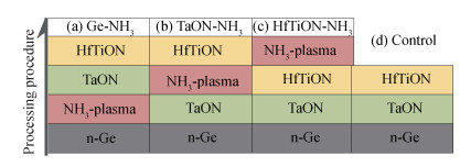
Fig. 1.
Schematic diagram of NH$_{\rm{3}}$ -plasma treatment at different stages of gate stack deposition.
SEMICONDUCTOR DEVICES
Xiaoyu Liu, Jingping Xu, Lu Liu, Zhixiang Cheng, Yong Huang and Jingkang Gong
Corresponding author: Jingping Xu, Email:jpxu@hust.edu.cn
Abstract: The effects of different NH3-plasma treatment procedures on interfacial and electrical properties of Ge MOS capacitors with stacked gate dielectric of HfTiON/TaON were investigated. The NH3-plasma treatment was performed at different steps during fabrication of the stacked gate dielectric, i.e. before or after interlayer (TaON) deposition, or after deposition of high-k dielectric (HfTiON). It was found that the excellent interface quality with an interface-state density of 4.79×10¹¹ eV-1cm-2 and low gate leakage current (3.43×10⁻⁵A/cm2 at Vg=1 V) could be achieved for the sample with NH3-plasma treatment directly on the Ge surface before TaON deposition. The involved mechanisms are attributed to the fact that the NH3-plasma can directly react with the Ge surface to form more Ge-N bonds, i.e. more GeOxNy, which effectively blocks the inter-diffusion of elements and suppresses the formation of unstable GeOx interfacial layer, and also passivates oxygen vacancies and dangling bonds near/at the interface due to more N incorporation and decomposed H atoms from the NH3-plasma.
Keywords: Ge MOS, NH3-plasma treatment, TaON interlayer, stacked gate dielectric
| [1] |
Goley P S, Hudait M K. Germanium based field-effect transistors:challenges and opportunities. Materials, 2014, 7(3):2301 doi: 10.3390/ma7032301
|
| [2] |
Ohno T, Nakayama D, Samukawa S. Al and Ge simultaneous oxidation using neutral beam post-oxidation for formation of gate stack structures. Appl Phys Lett, 2015, 107(13):133107 doi: 10.1063/1.4932385
|
| [3] |
Ji F, Xu J P, Lai P T, et al. Improved interfacial properties of Ge MOS capacitor with high-k dielectric by using TaON/GeON dual interlayer. IEEE Electron Device Lett, 2011, 32(2):122 doi: 10.1109/LED.2010.2092749
|
| [4] |
Xu J P, Zhang X F, Li C X, et al. Improved electrical properties of Ge p-MOSFET with gate dielectric by using interlayer. IEEE Electron Device Lett, 2008, 29(10):1155 doi: 10.1109/LED.2008.2004282
|
| [5] |
Li H, Guo Y, Robertson J. AlN-GeO2 based gate stack for improved reliability of Ge MOSFETs. Microelectron Eng, 2015, 147:168 doi: 10.1016/j.mee.2015.04.081
|
| [6] |
Gao F, Lee S J, Pan J S, et al. Surface passivation using ultrathin AlNx film for Ge-metal-oxide-semiconductor devices with hafnium oxide gate dielectric. Appl Phys Lett, 2005, 86(11):3501 doi: 10.1007/s11432-014-5180-y
|
| [7] |
Lee C H, Tabata T, Nishimura T, et al. Ge/GeO2 interface control with high pressure oxidation for improving electrical characteristics. Appl Phys Express, 2009, 2(7):071404 doi: 10.1143/APEX.2.071404/meta
|
| [8] |
Xie R, He W, Yu M, et al. Effects of fluorine incorporation and forming gas annealing on high-k gated germanium metal-oxide-semiconductor with GeO2 surface passivation. Appl Phys Lett, 2008, 93(7):3504 doi: 10.1063/1.2966367?journalCode=apl
|
| [9] |
Li X F, Liu X J, Cao Y Q, et al. Improved interfacial and electrical properties of atomic layer deposition HfO2 films on Ge with La2O3 passivation. Appl Surf Sci, 2013, 264:783 doi: 10.1016/j.apsusc.2012.10.127
|
| [10] |
Bethge O, Henkel C, Abermann S, et al. Stability of La2O3 and GeO2 passivated Ge surfaces during ALD of ZrO2 high-k dielectric. Appl Surf Sci, 2012, 258(8):3444 doi: 10.1016/j.apsusc.2011.11.094
|
| [11] |
Bethge O, Zimmermann C, Lutzer B, et al. Effective reduction of trap density at the Y2O3/Ge interface by rigorous high-temperature oxygen annealing. J Appl Phys, 2014, 116(21):214111 doi: 10.1063/1.4903533
|
| [12] |
Zimmermann C, Bethge O, Winkler K, et al. Improving the ALD-grown Y2O3/Ge interface quality by surface and annealing treatments. Appl Surf Sci, 2016, 369:377 doi: 10.1016/j.apsusc.2016.02.066
|
| [13] |
Chi X, Lan X, Lu C, et al. An improvement of HfO2/Ge interface by in situ remote N2 plasma pretreatment for Ge MOS devices. Mater Res Express, 2016, 3(3):035012 doi: 10.1088/2053-1591/3/3/035012
|
| [14] |
Lin M, Li M, An X, et al. Surface passivation of the Ge substrate by novel nitrogen plasma immersion treatment. Semicond Sci Tech, 2013, 28(8):085010 doi: 10.1088/0268-1242/28/8/085010
|
| [15] |
Sardashti K, Hu K T, Tang K, et al. Nitride passivation of the interface between high-k dielectrics and SiGe. Appl Phys Lett, 2016, 108(1):011604 doi: 10.1063/1.4939460
|
| [16] |
Xie Q, Musschoot J, Schaekers M, et al. Ultrathin GeOxNy interlayer formed by in situ NH3 plasma pretreatment for passivation of germanium metal-oxide-semiconductor devices. Appl Phys Lett, 2010, 97(22):2902 http://adsabs.harvard.edu/abs/2010ApPhL..97v2902X
|
| [17] |
Cao Y Q, Chen J, Liu X J, et al. HfO2/GeOxNy/Ge gate stacks with sub-nanometer capacitance equivalent thickness and low interface trap density by in situ NH3 plasma pretreatment. Appl Surf Sci, 2015, 325:13 doi: 10.1016/j.apsusc.2014.11.073
|
| [18] |
Cheng C C, Chien C H, Luo G L, et al. Study of thermal stability of HfOxNy/Ge capacitors using postdeposition annealing and NH3 plasma pretreatment. J Electrochem Soc, 2007, 154(7):G155 doi: 10.1149/1.2734875
|
| [19] |
Huang Y, Xu J P, Liu L, et al. N2-plasma-treated Ga2O3 (Gd2O3 as interface passivation layer for Ge MOS capacitor with HfTiON gate dielectric. IEEE Trans Electron Devices, 2016, 63(7):2838 doi: 10.1109/TED.2016.2565691
|
| [20] |
Xie R, Yu M, Lai M Y, et al. High-k gate stack on germanium substrate with fluorine incorporation. Appl Phys Lett, 2008, 92(16):3505 https://www.researchgate.net/publication/224406145_High-k_gate_stack_on_germanium_substrate_with_fluorine_incorporation
|
| [21] |
Kim G S, Kim S H, Kim J K, et al. Surface passivation of germanium using SF6 plasma to reduce source/drain contact resistance in germanium n-FET. IEEE Electron Device Lett, 2015, 36(8):745 doi: 10.1109/LED.2015.2440434
|
| [22] |
Oshima Y, Shandalov M, Sun Y, et al. Hafnium oxide/germanium oxynitride gate stacks on germanium:capacitance scaling and interface state density. Appl Phys Lett, 2009, 94(18):3102 doi: 10.1063/1.3116624
|
| [23] |
Oshima Y, Sun Y, Kuzum D, et al. Chemical bonding, interfaces, and defects in hafnium oxide/germanium oxynitride gate stacks on Ge (100). J Electrochem Soc, 2008, 155(12):G304 doi: 10.1149/1.2995832
|
| [24] |
Li C C, Chang-Liao K S, Fu C H, et al. Improved electrical characteristics high-k gated MOS devices with in-situ remote plasma treatment in atomic layer deposition. Microelectron Eng, 2013, 109:64 doi: 10.1016/j.mee.2013.03.060
|
| [25] |
Xu J P, Lai P T, Li C X, et al. Improved electrical properties of germanium MOS capacitors with gate dielectric grown in wet-NO ambient. IEEE Electron Device Lett, 2006, 27(6):439 doi: 10.1109/LED.2006.874124
|
| [26] |
Terman L M. An investigation of surface states at a silicon/silicon oxide interface employing metal-oxide-silicon diodes. Solid-State Electron, 1962, 5(5):285 doi: 10.1016/0038-1101(62)90111-9
|
| [27] |
Wang L S, Xu J P, Liu L, et al. Plasma-nitrided Ga2O3 (Gd2O3) as interfacial passivation layer for InGaAs metal-oxide-semiconductor capacitor with HfTiON gate dielectric. IEEE Trans Electron Devices, 2015, 62(4):1235 doi: 10.1109/TED.2015.2396972
|
| [28] |
Yuan W Y, Xu J P, Liu L, et al. Improved interfacial and electrical properties of Ge MOS devices with ZrON/GeON dual passivation layer. J Semicond, 2016, 37(5):054004 doi: 10.1088/1674-4926/37/5/054004
|
| [29] |
Taylor J A, Lancaster G M, Rabalais J W. Chemical reactions of N2+ ion beams with group Ⅳ elements and their oxides. J Electron Spectrosc Relat Phenom, 1978, 13(3):435 doi: 10.1016/0368-2048(78)85047-6
|
| [30] |
Chuang J C, Chen M C. Properties of thin Ta-N films reactively sputtered on Cu/SiO2/Si substrates. Thin Solid Films, 1998, 322(1):213 http://www.sciencedirect.com/science/article/pii/S0040609097009140
|
| [31] |
Larkins F P, Lubenfeld A. The Auger spectrum of solid ammonia. J Electron Spectrosc Relat Phenom, 1979, 15(1):137 doi: 10.1016/0368-2048(79)87024-3
|
| [32] |
Pashutski A, Folman M. Low temperature XPS studies of NO and N2O adsorption on Al (100). Surf Sci, 1989, 216(3):395 doi: 10.1016/0039-6028(89)90383-X
|
| [33] |
Wu N, Zhang Q C, Zhu C X, et al. Effect of surface NH3 anneal on the physical and electrical properties of HfO2 films on Ge substrate. Appl Phys Lett, 2004, 84(19):3741 doi: 10.1063/1.1737057
|
| [34] |
Ji F, Xu J P, Huang Y, et al. Improved interfacial and electrical properties of Ge-based metal-oxide-semiconductor capacitor with LaTaON passivation layer. IEEE Trans Electron Devices, 2014, 61(11):3608 doi: 10.1109/TED.2014.2356597
|
| [35] |
Suzuki A, Nonaka H. Plasma diagnostics for NH3 plasmas using a quartz sensor at various pressures. Jpn J Appl Phys, 2011, 50(1S1):01AA03 doi: 10.7567/JJAP.50.01AA03
|
| [36] |
Yasui K, Arayama T, Okutani S, et al. Generation of ammonia plasma using a helical antenna and nitridation of GaAs surface. Appl Surf Sci, 2003, 212:619 http://www.sciencedirect.com/science/article/pii/S0169433203001351
|
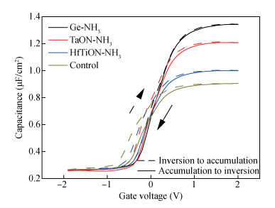
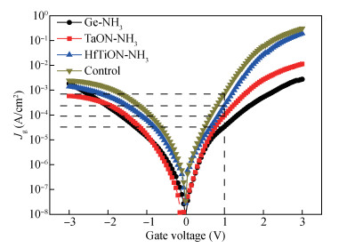
Table 1.
Electrical and physical parameters extracted from HF

|
Table 2. Energy position and atomic percentage of the species in Fig. 6.

|
| [1] |
Goley P S, Hudait M K. Germanium based field-effect transistors:challenges and opportunities. Materials, 2014, 7(3):2301 doi: 10.3390/ma7032301
|
| [2] |
Ohno T, Nakayama D, Samukawa S. Al and Ge simultaneous oxidation using neutral beam post-oxidation for formation of gate stack structures. Appl Phys Lett, 2015, 107(13):133107 doi: 10.1063/1.4932385
|
| [3] |
Ji F, Xu J P, Lai P T, et al. Improved interfacial properties of Ge MOS capacitor with high-k dielectric by using TaON/GeON dual interlayer. IEEE Electron Device Lett, 2011, 32(2):122 doi: 10.1109/LED.2010.2092749
|
| [4] |
Xu J P, Zhang X F, Li C X, et al. Improved electrical properties of Ge p-MOSFET with gate dielectric by using interlayer. IEEE Electron Device Lett, 2008, 29(10):1155 doi: 10.1109/LED.2008.2004282
|
| [5] |
Li H, Guo Y, Robertson J. AlN-GeO2 based gate stack for improved reliability of Ge MOSFETs. Microelectron Eng, 2015, 147:168 doi: 10.1016/j.mee.2015.04.081
|
| [6] |
Gao F, Lee S J, Pan J S, et al. Surface passivation using ultrathin AlNx film for Ge-metal-oxide-semiconductor devices with hafnium oxide gate dielectric. Appl Phys Lett, 2005, 86(11):3501 doi: 10.1007/s11432-014-5180-y
|
| [7] |
Lee C H, Tabata T, Nishimura T, et al. Ge/GeO2 interface control with high pressure oxidation for improving electrical characteristics. Appl Phys Express, 2009, 2(7):071404 doi: 10.1143/APEX.2.071404/meta
|
| [8] |
Xie R, He W, Yu M, et al. Effects of fluorine incorporation and forming gas annealing on high-k gated germanium metal-oxide-semiconductor with GeO2 surface passivation. Appl Phys Lett, 2008, 93(7):3504 doi: 10.1063/1.2966367?journalCode=apl
|
| [9] |
Li X F, Liu X J, Cao Y Q, et al. Improved interfacial and electrical properties of atomic layer deposition HfO2 films on Ge with La2O3 passivation. Appl Surf Sci, 2013, 264:783 doi: 10.1016/j.apsusc.2012.10.127
|
| [10] |
Bethge O, Henkel C, Abermann S, et al. Stability of La2O3 and GeO2 passivated Ge surfaces during ALD of ZrO2 high-k dielectric. Appl Surf Sci, 2012, 258(8):3444 doi: 10.1016/j.apsusc.2011.11.094
|
| [11] |
Bethge O, Zimmermann C, Lutzer B, et al. Effective reduction of trap density at the Y2O3/Ge interface by rigorous high-temperature oxygen annealing. J Appl Phys, 2014, 116(21):214111 doi: 10.1063/1.4903533
|
| [12] |
Zimmermann C, Bethge O, Winkler K, et al. Improving the ALD-grown Y2O3/Ge interface quality by surface and annealing treatments. Appl Surf Sci, 2016, 369:377 doi: 10.1016/j.apsusc.2016.02.066
|
| [13] |
Chi X, Lan X, Lu C, et al. An improvement of HfO2/Ge interface by in situ remote N2 plasma pretreatment for Ge MOS devices. Mater Res Express, 2016, 3(3):035012 doi: 10.1088/2053-1591/3/3/035012
|
| [14] |
Lin M, Li M, An X, et al. Surface passivation of the Ge substrate by novel nitrogen plasma immersion treatment. Semicond Sci Tech, 2013, 28(8):085010 doi: 10.1088/0268-1242/28/8/085010
|
| [15] |
Sardashti K, Hu K T, Tang K, et al. Nitride passivation of the interface between high-k dielectrics and SiGe. Appl Phys Lett, 2016, 108(1):011604 doi: 10.1063/1.4939460
|
| [16] |
Xie Q, Musschoot J, Schaekers M, et al. Ultrathin GeOxNy interlayer formed by in situ NH3 plasma pretreatment for passivation of germanium metal-oxide-semiconductor devices. Appl Phys Lett, 2010, 97(22):2902 http://adsabs.harvard.edu/abs/2010ApPhL..97v2902X
|
| [17] |
Cao Y Q, Chen J, Liu X J, et al. HfO2/GeOxNy/Ge gate stacks with sub-nanometer capacitance equivalent thickness and low interface trap density by in situ NH3 plasma pretreatment. Appl Surf Sci, 2015, 325:13 doi: 10.1016/j.apsusc.2014.11.073
|
| [18] |
Cheng C C, Chien C H, Luo G L, et al. Study of thermal stability of HfOxNy/Ge capacitors using postdeposition annealing and NH3 plasma pretreatment. J Electrochem Soc, 2007, 154(7):G155 doi: 10.1149/1.2734875
|
| [19] |
Huang Y, Xu J P, Liu L, et al. N2-plasma-treated Ga2O3 (Gd2O3 as interface passivation layer for Ge MOS capacitor with HfTiON gate dielectric. IEEE Trans Electron Devices, 2016, 63(7):2838 doi: 10.1109/TED.2016.2565691
|
| [20] |
Xie R, Yu M, Lai M Y, et al. High-k gate stack on germanium substrate with fluorine incorporation. Appl Phys Lett, 2008, 92(16):3505 https://www.researchgate.net/publication/224406145_High-k_gate_stack_on_germanium_substrate_with_fluorine_incorporation
|
| [21] |
Kim G S, Kim S H, Kim J K, et al. Surface passivation of germanium using SF6 plasma to reduce source/drain contact resistance in germanium n-FET. IEEE Electron Device Lett, 2015, 36(8):745 doi: 10.1109/LED.2015.2440434
|
| [22] |
Oshima Y, Shandalov M, Sun Y, et al. Hafnium oxide/germanium oxynitride gate stacks on germanium:capacitance scaling and interface state density. Appl Phys Lett, 2009, 94(18):3102 doi: 10.1063/1.3116624
|
| [23] |
Oshima Y, Sun Y, Kuzum D, et al. Chemical bonding, interfaces, and defects in hafnium oxide/germanium oxynitride gate stacks on Ge (100). J Electrochem Soc, 2008, 155(12):G304 doi: 10.1149/1.2995832
|
| [24] |
Li C C, Chang-Liao K S, Fu C H, et al. Improved electrical characteristics high-k gated MOS devices with in-situ remote plasma treatment in atomic layer deposition. Microelectron Eng, 2013, 109:64 doi: 10.1016/j.mee.2013.03.060
|
| [25] |
Xu J P, Lai P T, Li C X, et al. Improved electrical properties of germanium MOS capacitors with gate dielectric grown in wet-NO ambient. IEEE Electron Device Lett, 2006, 27(6):439 doi: 10.1109/LED.2006.874124
|
| [26] |
Terman L M. An investigation of surface states at a silicon/silicon oxide interface employing metal-oxide-silicon diodes. Solid-State Electron, 1962, 5(5):285 doi: 10.1016/0038-1101(62)90111-9
|
| [27] |
Wang L S, Xu J P, Liu L, et al. Plasma-nitrided Ga2O3 (Gd2O3) as interfacial passivation layer for InGaAs metal-oxide-semiconductor capacitor with HfTiON gate dielectric. IEEE Trans Electron Devices, 2015, 62(4):1235 doi: 10.1109/TED.2015.2396972
|
| [28] |
Yuan W Y, Xu J P, Liu L, et al. Improved interfacial and electrical properties of Ge MOS devices with ZrON/GeON dual passivation layer. J Semicond, 2016, 37(5):054004 doi: 10.1088/1674-4926/37/5/054004
|
| [29] |
Taylor J A, Lancaster G M, Rabalais J W. Chemical reactions of N2+ ion beams with group Ⅳ elements and their oxides. J Electron Spectrosc Relat Phenom, 1978, 13(3):435 doi: 10.1016/0368-2048(78)85047-6
|
| [30] |
Chuang J C, Chen M C. Properties of thin Ta-N films reactively sputtered on Cu/SiO2/Si substrates. Thin Solid Films, 1998, 322(1):213 http://www.sciencedirect.com/science/article/pii/S0040609097009140
|
| [31] |
Larkins F P, Lubenfeld A. The Auger spectrum of solid ammonia. J Electron Spectrosc Relat Phenom, 1979, 15(1):137 doi: 10.1016/0368-2048(79)87024-3
|
| [32] |
Pashutski A, Folman M. Low temperature XPS studies of NO and N2O adsorption on Al (100). Surf Sci, 1989, 216(3):395 doi: 10.1016/0039-6028(89)90383-X
|
| [33] |
Wu N, Zhang Q C, Zhu C X, et al. Effect of surface NH3 anneal on the physical and electrical properties of HfO2 films on Ge substrate. Appl Phys Lett, 2004, 84(19):3741 doi: 10.1063/1.1737057
|
| [34] |
Ji F, Xu J P, Huang Y, et al. Improved interfacial and electrical properties of Ge-based metal-oxide-semiconductor capacitor with LaTaON passivation layer. IEEE Trans Electron Devices, 2014, 61(11):3608 doi: 10.1109/TED.2014.2356597
|
| [35] |
Suzuki A, Nonaka H. Plasma diagnostics for NH3 plasmas using a quartz sensor at various pressures. Jpn J Appl Phys, 2011, 50(1S1):01AA03 doi: 10.7567/JJAP.50.01AA03
|
| [36] |
Yasui K, Arayama T, Okutani S, et al. Generation of ammonia plasma using a helical antenna and nitridation of GaAs surface. Appl Surf Sci, 2003, 212:619 http://www.sciencedirect.com/science/article/pii/S0169433203001351
|


Article views: 3793 Times PDF downloads: 40 Times Cited by: 0 Times
Received: 13 October 2016 Revised: 18 February 2017 Online: Published: 01 August 2017
| Citation: |
Xiaoyu Liu, Jingping Xu, Lu Liu, Zhixiang Cheng, Yong Huang, Jingkang Gong. Investigation on interfacial and electrical properties of Ge MOS capacitor with different NH3-plasma treatment procedure[J]. Journal of Semiconductors, 2017, 38(8): 084004. doi: 10.1088/1674-4926/38/8/084004
****
X Y Liu, J P Xu, L Liu, Z X Cheng, Y Huang, J K Gong. Investigation on interfacial and electrical properties of Ge MOS capacitor with different NH3-plasma treatment procedure[J]. J. Semicond., 2017, 38(8): 084004. doi: 10.1088/1674-4926/38/8/084004.

|
| [1] |
Goley P S, Hudait M K. Germanium based field-effect transistors:challenges and opportunities. Materials, 2014, 7(3):2301 doi: 10.3390/ma7032301
|
| [2] |
Ohno T, Nakayama D, Samukawa S. Al and Ge simultaneous oxidation using neutral beam post-oxidation for formation of gate stack structures. Appl Phys Lett, 2015, 107(13):133107 doi: 10.1063/1.4932385
|
| [3] |
Ji F, Xu J P, Lai P T, et al. Improved interfacial properties of Ge MOS capacitor with high-k dielectric by using TaON/GeON dual interlayer. IEEE Electron Device Lett, 2011, 32(2):122 doi: 10.1109/LED.2010.2092749
|
| [4] |
Xu J P, Zhang X F, Li C X, et al. Improved electrical properties of Ge p-MOSFET with gate dielectric by using interlayer. IEEE Electron Device Lett, 2008, 29(10):1155 doi: 10.1109/LED.2008.2004282
|
| [5] |
Li H, Guo Y, Robertson J. AlN-GeO2 based gate stack for improved reliability of Ge MOSFETs. Microelectron Eng, 2015, 147:168 doi: 10.1016/j.mee.2015.04.081
|
| [6] |
Gao F, Lee S J, Pan J S, et al. Surface passivation using ultrathin AlNx film for Ge-metal-oxide-semiconductor devices with hafnium oxide gate dielectric. Appl Phys Lett, 2005, 86(11):3501 doi: 10.1007/s11432-014-5180-y
|
| [7] |
Lee C H, Tabata T, Nishimura T, et al. Ge/GeO2 interface control with high pressure oxidation for improving electrical characteristics. Appl Phys Express, 2009, 2(7):071404 doi: 10.1143/APEX.2.071404/meta
|
| [8] |
Xie R, He W, Yu M, et al. Effects of fluorine incorporation and forming gas annealing on high-k gated germanium metal-oxide-semiconductor with GeO2 surface passivation. Appl Phys Lett, 2008, 93(7):3504 doi: 10.1063/1.2966367?journalCode=apl
|
| [9] |
Li X F, Liu X J, Cao Y Q, et al. Improved interfacial and electrical properties of atomic layer deposition HfO2 films on Ge with La2O3 passivation. Appl Surf Sci, 2013, 264:783 doi: 10.1016/j.apsusc.2012.10.127
|
| [10] |
Bethge O, Henkel C, Abermann S, et al. Stability of La2O3 and GeO2 passivated Ge surfaces during ALD of ZrO2 high-k dielectric. Appl Surf Sci, 2012, 258(8):3444 doi: 10.1016/j.apsusc.2011.11.094
|
| [11] |
Bethge O, Zimmermann C, Lutzer B, et al. Effective reduction of trap density at the Y2O3/Ge interface by rigorous high-temperature oxygen annealing. J Appl Phys, 2014, 116(21):214111 doi: 10.1063/1.4903533
|
| [12] |
Zimmermann C, Bethge O, Winkler K, et al. Improving the ALD-grown Y2O3/Ge interface quality by surface and annealing treatments. Appl Surf Sci, 2016, 369:377 doi: 10.1016/j.apsusc.2016.02.066
|
| [13] |
Chi X, Lan X, Lu C, et al. An improvement of HfO2/Ge interface by in situ remote N2 plasma pretreatment for Ge MOS devices. Mater Res Express, 2016, 3(3):035012 doi: 10.1088/2053-1591/3/3/035012
|
| [14] |
Lin M, Li M, An X, et al. Surface passivation of the Ge substrate by novel nitrogen plasma immersion treatment. Semicond Sci Tech, 2013, 28(8):085010 doi: 10.1088/0268-1242/28/8/085010
|
| [15] |
Sardashti K, Hu K T, Tang K, et al. Nitride passivation of the interface between high-k dielectrics and SiGe. Appl Phys Lett, 2016, 108(1):011604 doi: 10.1063/1.4939460
|
| [16] |
Xie Q, Musschoot J, Schaekers M, et al. Ultrathin GeOxNy interlayer formed by in situ NH3 plasma pretreatment for passivation of germanium metal-oxide-semiconductor devices. Appl Phys Lett, 2010, 97(22):2902 http://adsabs.harvard.edu/abs/2010ApPhL..97v2902X
|
| [17] |
Cao Y Q, Chen J, Liu X J, et al. HfO2/GeOxNy/Ge gate stacks with sub-nanometer capacitance equivalent thickness and low interface trap density by in situ NH3 plasma pretreatment. Appl Surf Sci, 2015, 325:13 doi: 10.1016/j.apsusc.2014.11.073
|
| [18] |
Cheng C C, Chien C H, Luo G L, et al. Study of thermal stability of HfOxNy/Ge capacitors using postdeposition annealing and NH3 plasma pretreatment. J Electrochem Soc, 2007, 154(7):G155 doi: 10.1149/1.2734875
|
| [19] |
Huang Y, Xu J P, Liu L, et al. N2-plasma-treated Ga2O3 (Gd2O3 as interface passivation layer for Ge MOS capacitor with HfTiON gate dielectric. IEEE Trans Electron Devices, 2016, 63(7):2838 doi: 10.1109/TED.2016.2565691
|
| [20] |
Xie R, Yu M, Lai M Y, et al. High-k gate stack on germanium substrate with fluorine incorporation. Appl Phys Lett, 2008, 92(16):3505 https://www.researchgate.net/publication/224406145_High-k_gate_stack_on_germanium_substrate_with_fluorine_incorporation
|
| [21] |
Kim G S, Kim S H, Kim J K, et al. Surface passivation of germanium using SF6 plasma to reduce source/drain contact resistance in germanium n-FET. IEEE Electron Device Lett, 2015, 36(8):745 doi: 10.1109/LED.2015.2440434
|
| [22] |
Oshima Y, Shandalov M, Sun Y, et al. Hafnium oxide/germanium oxynitride gate stacks on germanium:capacitance scaling and interface state density. Appl Phys Lett, 2009, 94(18):3102 doi: 10.1063/1.3116624
|
| [23] |
Oshima Y, Sun Y, Kuzum D, et al. Chemical bonding, interfaces, and defects in hafnium oxide/germanium oxynitride gate stacks on Ge (100). J Electrochem Soc, 2008, 155(12):G304 doi: 10.1149/1.2995832
|
| [24] |
Li C C, Chang-Liao K S, Fu C H, et al. Improved electrical characteristics high-k gated MOS devices with in-situ remote plasma treatment in atomic layer deposition. Microelectron Eng, 2013, 109:64 doi: 10.1016/j.mee.2013.03.060
|
| [25] |
Xu J P, Lai P T, Li C X, et al. Improved electrical properties of germanium MOS capacitors with gate dielectric grown in wet-NO ambient. IEEE Electron Device Lett, 2006, 27(6):439 doi: 10.1109/LED.2006.874124
|
| [26] |
Terman L M. An investigation of surface states at a silicon/silicon oxide interface employing metal-oxide-silicon diodes. Solid-State Electron, 1962, 5(5):285 doi: 10.1016/0038-1101(62)90111-9
|
| [27] |
Wang L S, Xu J P, Liu L, et al. Plasma-nitrided Ga2O3 (Gd2O3) as interfacial passivation layer for InGaAs metal-oxide-semiconductor capacitor with HfTiON gate dielectric. IEEE Trans Electron Devices, 2015, 62(4):1235 doi: 10.1109/TED.2015.2396972
|
| [28] |
Yuan W Y, Xu J P, Liu L, et al. Improved interfacial and electrical properties of Ge MOS devices with ZrON/GeON dual passivation layer. J Semicond, 2016, 37(5):054004 doi: 10.1088/1674-4926/37/5/054004
|
| [29] |
Taylor J A, Lancaster G M, Rabalais J W. Chemical reactions of N2+ ion beams with group Ⅳ elements and their oxides. J Electron Spectrosc Relat Phenom, 1978, 13(3):435 doi: 10.1016/0368-2048(78)85047-6
|
| [30] |
Chuang J C, Chen M C. Properties of thin Ta-N films reactively sputtered on Cu/SiO2/Si substrates. Thin Solid Films, 1998, 322(1):213 http://www.sciencedirect.com/science/article/pii/S0040609097009140
|
| [31] |
Larkins F P, Lubenfeld A. The Auger spectrum of solid ammonia. J Electron Spectrosc Relat Phenom, 1979, 15(1):137 doi: 10.1016/0368-2048(79)87024-3
|
| [32] |
Pashutski A, Folman M. Low temperature XPS studies of NO and N2O adsorption on Al (100). Surf Sci, 1989, 216(3):395 doi: 10.1016/0039-6028(89)90383-X
|
| [33] |
Wu N, Zhang Q C, Zhu C X, et al. Effect of surface NH3 anneal on the physical and electrical properties of HfO2 films on Ge substrate. Appl Phys Lett, 2004, 84(19):3741 doi: 10.1063/1.1737057
|
| [34] |
Ji F, Xu J P, Huang Y, et al. Improved interfacial and electrical properties of Ge-based metal-oxide-semiconductor capacitor with LaTaON passivation layer. IEEE Trans Electron Devices, 2014, 61(11):3608 doi: 10.1109/TED.2014.2356597
|
| [35] |
Suzuki A, Nonaka H. Plasma diagnostics for NH3 plasmas using a quartz sensor at various pressures. Jpn J Appl Phys, 2011, 50(1S1):01AA03 doi: 10.7567/JJAP.50.01AA03
|
| [36] |
Yasui K, Arayama T, Okutani S, et al. Generation of ammonia plasma using a helical antenna and nitridation of GaAs surface. Appl Surf Sci, 2003, 212:619 http://www.sciencedirect.com/science/article/pii/S0169433203001351
|

 WeChat ID
Journal of Semiconductors © 2017 All Rights Reserved 京ICP备05085259号-2

 DownLoad:

