


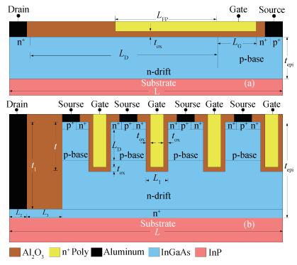
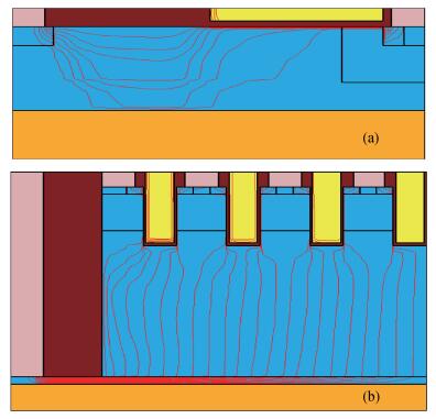
Fig. 1.
(Color online) The cross-sectional view of (a) conventional and (b) proposed structure.
SEMICONDUCTOR DEVICES
Corresponding author: Y. Singh, Email: om_ysingh@yahoo.co.in
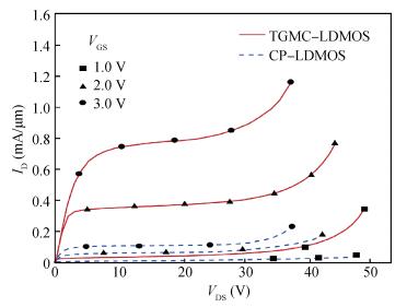
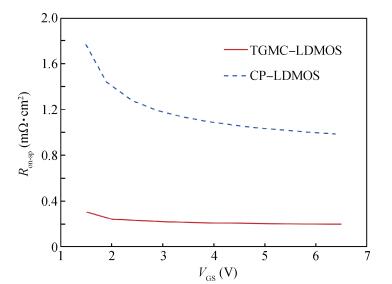
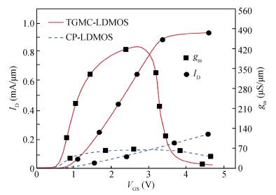
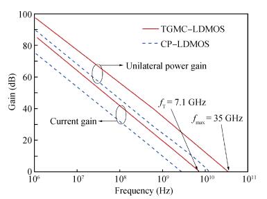
Abstract: In this work, a new RF power trench-gate multi-channel laterally-diffused MOSFET (TGMC-LDMOS) on InGaAs is proposed. The gate-electrodes of the new structure are placed vertically in the trenches built in the drift layer. Each gate results in the formation of two channels in the p-body region of the device. The drain metal is also placed in a trench to take contact from the n+-InGaAs region located over the substrate. In a cell length of 5 μm, the TGMC-LDMOS structure has seven channels, which conduct simultaneously to carry drain current in parallel. The formation of multi-channels in the proposed device increases the drive current (ID) leading to a large reduction in the specific on-resistance (Ron-sp). Due to better control of gates on the drain current, the new structure exhibits substantially higher transconductance (gm) resulting in significant improvement in cut-off frequency (fT) and oscillation frequency (fmax). Using two-dimensional numerical simulations, a 55 V TGMC-LDMOS is demonstrated to achieve 7 times higher ID, 6.2 times lower Ron-sp, 6.3 times higher peak gm, 2.6 times higher fT, and 2.5 times increase in fmax in comparison to a conventional device for the identical cell length.
Keywords: InGaAs, trench-gate, multi-channel, RF LDMOS
| [1] |
Darabi H. Radio frequency integrated circuits and systems. Cambridge University Press, 2015
|
| [2] |
Erlbacher T. Lateral power transistors in integrated circuits. Springer Int Pub, 2014
|
| [3] |
Baliga B J. Silicon RF power MOSFETs. Singapore: World Scientific, 2005
|
| [4] |
Orouji A A, Pak A. Numerical simulation of lateral diffused metal oxide semiconductor field effect transistors:a novel technique for electric field control to improve breakdown voltage. Mater Sci Semi Process, 2015, 34:230 doi: 10.1016/j.mssp.2015.02.027
|
| [5] |
Sandeep S, Komaragiri R. Drift region optimization by double epitaxial layer in low and medium power rated silicon power MOSFETs. J Mater Sci Mater Electron, 2015, 26:230 doi: 10.1007/s10856-015-5561-9
|
| [6] |
Punetha M, Singh Y. A 100 V high-performance SOI trench LDMOS with low cell pitch. J Electron Mater, 2015, 10:3388 doi: 10.1007/s11664-015-3834-1
|
| [7] |
Singh Y, Punetha M. A lateral trench dual gate power MOSFET on thin SOI for improved performance. J Solid State Sci Tech, 2013, 2:Q113 doi: 10.1149/2.021307jss
|
| [8] |
Singh Y, Rawat R S. High figure-of-merit SOI power LDMOS for power integrated circuits. Eng Sci Tech Int J, 2015, 18:141 doi: 10.1016/j.jestch.2014.10.004
|
| [9] |
Hu Y, Wang G, Chang S, et al. Effect of silicon window polarity on partial-SOI LDMOSFETs. Micro Nano Lett, 2012, 7:628 doi: 10.1049/mnl.2012.0351
|
| [10] |
Du W, Lyu X, Chen X. An LDMOS with large SOA and low specific on-resistance. J Semicond, 2016, 37:054006 doi: 10.1088/1674-4926/37/5/054006
|
| [11] |
Xu Q, Luo X, Zhou K, et al. Ultralow specific on-resistance high voltage trench SOI LDMOS with enhanced RESURF effect. J Semicond, 2015, 36(2):024010 doi: 10.1088/1674-4926/36/2/024010
|
| [12] |
Fan Y, Luo X, Zhou K, et al. An L-shaped low on-resistance current path SOI LDMOS with dielectric field enhancement. J Semicond, 2014, 35(3):034011 doi: 10.1088/1674-4926/35/3/034011
|
| [13] |
Luo X, Wang X, Hu G, et al. Experimental and theoretical study of an improved breakdown voltage SOI LDMOS with a reduced cell pitch. J Semicond, 2014, 35(2):024007 doi: 10.1088/1674-4926/35/2/024007
|
| [14] |
Ge R, Luo X, Jiang Y, et al. A low on-resistance SOI LDMOS using a trench gate and a recessed drain. J Semicond, 2012, 33(7):074005 doi: 10.1088/1674-4926/33/7/074005
|
| [15] |
Hu X, Zhang B, Luo X, et al. A new high voltage SOI LDMOS with triple RESURF structure. J Semicond, 2011, 32(7):074006 doi: 10.1088/1674-4926/32/7/074006
|
| [16] |
Payal M, Singh Y. A multi-channel trench-gate (MCTG) RF LDMOS on SOI. IETE Tech Rev, 2016:1 doi: 10.1080/02564602.2016.1166993
|
| [17] |
Yu T, Luo L. An RF LDMOS with excellent efficiency and ruggedness based on a modified CMOS process. J Semicond, 2013, 34(9):094007 doi: 10.1088/1674-4926/34/9/094007
|
| [18] |
Punetha M, Singh Y. SOI dual-gate trench LDMOSFET for RF integrated power amplifiers. IETE Tech Rev, 2016:1 doi: 10.1080/02564602.2016.1199978?journalCode=titr20
|
| [19] |
Punetha M, Singh Y. Dual-channel trench LDMOS on SOI for RF power amplifier applications. J Comput Electron, 2015, 15:639
|
| [20] |
Chen K M, Huang G W, Chen B Y, et al. LDMOS transistor high-frequency performance enhancements by strain. IEEE Electron Device Lett, 2012, 33:471 doi: 10.1109/LED.2011.2182494
|
| [21] |
Chen K M, Chen B Y, Chiu C S, et al. Performance improvement in RF LDMOS transistors using wider drain contact. IEEE Electron Device Lett, 2013, 34:1085 doi: 10.1109/LED.2013.2272937
|
| [22] |
Yang R, Li J F, Qian H, et al. A short-channel SOI RF power LDMOS technology with TiSi2 salicide on dual sidewalls with cutoff frequency fT 19.3 GHz. IEEE Electron Device Lett, 2006, 27:917 doi: 10.1109/LED.2006.883561
|
| [23] |
Seoane N, Garcia-Loureiro A J, Kalna K, et al. Random dopant related variability in the 30 nm gate length In0.75Ga0.25As implant free MOSFET. J Comput Electron, 2008, 7:159 doi: 10.1007/s10825-008-0233-3
|
| [24] |
Adhikari M S, Singh Y. High-performance dual-channel InGaAs MOSFET for small signal RF applications. Electron Lett, 2015, 51:1203 doi: 10.1049/el.2015.0980
|
| [25] |
Dehzangi A, Wee M F M R, Wichmann N, et al. Threshold voltage study of scaled self-aligned In0.53Ga0.47As metal oxide semiconductor field effect transistor for different source/drain doping concentrations. Micro Nano Lett, 2014, 9:181
|
| [26] |
Zhou J H, Chang H D, Zhang X F, et al. Fabrication of a novel RF switch device with high performance using In0.4Ga0.6As MOSFET technology. J Semicond, 2016, 37:024005 doi: 10.1088/1674-4926/37/2/024005
|
| [27] |
Steighner J B, Yuan J S, Liu Y. Simulation and analysis of InGaAs power MOSFET performances and reliability. IEEE Trans Electron Device, 2011, 58:180 doi: 10.1109/TED.2010.2089460
|
| [28] |
Singh Y, Badiyari M. Performance optimization of InGaAs power LDMOSFET. Microelectron J, 2015, 5:404 http://www.sciencedirect.com/science/article/pii/S0026269215000439
|
| [29] |
Adhikari M S, Singh Y. High performance DCTG-LDMOS on InGaAs for RF power amplifier applications. Mater Sci Semi Process, 2015, 40:861 doi: 10.1016/j.mssp.2015.07.067
|
| [30] |
Singh Y, Adhikari M S. Performance evaluation of a lateral trench-gate power MOSFET on InGaAs. J Comput Electron, 2014, 13:155 doi: 10.1007/s10825-013-0493-4
|
| [31] |
ATLAS user's manual: device simulation software, Silvaco Int. , Santa Clara, CA 2010
|


Article views: 4069 Times PDF downloads: 29 Times Cited by: 0 Times
Received: 18 November 2016 Revised: 16 February 2017 Online: Published: 01 September 2017
| Citation: |
M. Payal, Y. Singh. A new RF trench-gate multi-channel laterally-diffused MOSFET on InGaAs[J]. Journal of Semiconductors, 2017, 38(9): 094001. doi: 10.1088/1674-4926/38/9/094001
****
M. Payal, Y. Singh. A new RF trench-gate multi-channel laterally-diffused MOSFET on InGaAs[J]. J. Semicond., 2017, 38(9): 094001. doi: 10.1088/1674-4926/38/9/094001.

|
| [1] |
Darabi H. Radio frequency integrated circuits and systems. Cambridge University Press, 2015
|
| [2] |
Erlbacher T. Lateral power transistors in integrated circuits. Springer Int Pub, 2014
|
| [3] |
Baliga B J. Silicon RF power MOSFETs. Singapore: World Scientific, 2005
|
| [4] |
Orouji A A, Pak A. Numerical simulation of lateral diffused metal oxide semiconductor field effect transistors:a novel technique for electric field control to improve breakdown voltage. Mater Sci Semi Process, 2015, 34:230 doi: 10.1016/j.mssp.2015.02.027
|
| [5] |
Sandeep S, Komaragiri R. Drift region optimization by double epitaxial layer in low and medium power rated silicon power MOSFETs. J Mater Sci Mater Electron, 2015, 26:230 doi: 10.1007/s10856-015-5561-9
|
| [6] |
Punetha M, Singh Y. A 100 V high-performance SOI trench LDMOS with low cell pitch. J Electron Mater, 2015, 10:3388 doi: 10.1007/s11664-015-3834-1
|
| [7] |
Singh Y, Punetha M. A lateral trench dual gate power MOSFET on thin SOI for improved performance. J Solid State Sci Tech, 2013, 2:Q113 doi: 10.1149/2.021307jss
|
| [8] |
Singh Y, Rawat R S. High figure-of-merit SOI power LDMOS for power integrated circuits. Eng Sci Tech Int J, 2015, 18:141 doi: 10.1016/j.jestch.2014.10.004
|
| [9] |
Hu Y, Wang G, Chang S, et al. Effect of silicon window polarity on partial-SOI LDMOSFETs. Micro Nano Lett, 2012, 7:628 doi: 10.1049/mnl.2012.0351
|
| [10] |
Du W, Lyu X, Chen X. An LDMOS with large SOA and low specific on-resistance. J Semicond, 2016, 37:054006 doi: 10.1088/1674-4926/37/5/054006
|
| [11] |
Xu Q, Luo X, Zhou K, et al. Ultralow specific on-resistance high voltage trench SOI LDMOS with enhanced RESURF effect. J Semicond, 2015, 36(2):024010 doi: 10.1088/1674-4926/36/2/024010
|
| [12] |
Fan Y, Luo X, Zhou K, et al. An L-shaped low on-resistance current path SOI LDMOS with dielectric field enhancement. J Semicond, 2014, 35(3):034011 doi: 10.1088/1674-4926/35/3/034011
|
| [13] |
Luo X, Wang X, Hu G, et al. Experimental and theoretical study of an improved breakdown voltage SOI LDMOS with a reduced cell pitch. J Semicond, 2014, 35(2):024007 doi: 10.1088/1674-4926/35/2/024007
|
| [14] |
Ge R, Luo X, Jiang Y, et al. A low on-resistance SOI LDMOS using a trench gate and a recessed drain. J Semicond, 2012, 33(7):074005 doi: 10.1088/1674-4926/33/7/074005
|
| [15] |
Hu X, Zhang B, Luo X, et al. A new high voltage SOI LDMOS with triple RESURF structure. J Semicond, 2011, 32(7):074006 doi: 10.1088/1674-4926/32/7/074006
|
| [16] |
Payal M, Singh Y. A multi-channel trench-gate (MCTG) RF LDMOS on SOI. IETE Tech Rev, 2016:1 doi: 10.1080/02564602.2016.1166993
|
| [17] |
Yu T, Luo L. An RF LDMOS with excellent efficiency and ruggedness based on a modified CMOS process. J Semicond, 2013, 34(9):094007 doi: 10.1088/1674-4926/34/9/094007
|
| [18] |
Punetha M, Singh Y. SOI dual-gate trench LDMOSFET for RF integrated power amplifiers. IETE Tech Rev, 2016:1 doi: 10.1080/02564602.2016.1199978?journalCode=titr20
|
| [19] |
Punetha M, Singh Y. Dual-channel trench LDMOS on SOI for RF power amplifier applications. J Comput Electron, 2015, 15:639
|
| [20] |
Chen K M, Huang G W, Chen B Y, et al. LDMOS transistor high-frequency performance enhancements by strain. IEEE Electron Device Lett, 2012, 33:471 doi: 10.1109/LED.2011.2182494
|
| [21] |
Chen K M, Chen B Y, Chiu C S, et al. Performance improvement in RF LDMOS transistors using wider drain contact. IEEE Electron Device Lett, 2013, 34:1085 doi: 10.1109/LED.2013.2272937
|
| [22] |
Yang R, Li J F, Qian H, et al. A short-channel SOI RF power LDMOS technology with TiSi2 salicide on dual sidewalls with cutoff frequency fT 19.3 GHz. IEEE Electron Device Lett, 2006, 27:917 doi: 10.1109/LED.2006.883561
|
| [23] |
Seoane N, Garcia-Loureiro A J, Kalna K, et al. Random dopant related variability in the 30 nm gate length In0.75Ga0.25As implant free MOSFET. J Comput Electron, 2008, 7:159 doi: 10.1007/s10825-008-0233-3
|
| [24] |
Adhikari M S, Singh Y. High-performance dual-channel InGaAs MOSFET for small signal RF applications. Electron Lett, 2015, 51:1203 doi: 10.1049/el.2015.0980
|
| [25] |
Dehzangi A, Wee M F M R, Wichmann N, et al. Threshold voltage study of scaled self-aligned In0.53Ga0.47As metal oxide semiconductor field effect transistor for different source/drain doping concentrations. Micro Nano Lett, 2014, 9:181
|
| [26] |
Zhou J H, Chang H D, Zhang X F, et al. Fabrication of a novel RF switch device with high performance using In0.4Ga0.6As MOSFET technology. J Semicond, 2016, 37:024005 doi: 10.1088/1674-4926/37/2/024005
|
| [27] |
Steighner J B, Yuan J S, Liu Y. Simulation and analysis of InGaAs power MOSFET performances and reliability. IEEE Trans Electron Device, 2011, 58:180 doi: 10.1109/TED.2010.2089460
|
| [28] |
Singh Y, Badiyari M. Performance optimization of InGaAs power LDMOSFET. Microelectron J, 2015, 5:404 http://www.sciencedirect.com/science/article/pii/S0026269215000439
|
| [29] |
Adhikari M S, Singh Y. High performance DCTG-LDMOS on InGaAs for RF power amplifier applications. Mater Sci Semi Process, 2015, 40:861 doi: 10.1016/j.mssp.2015.07.067
|
| [30] |
Singh Y, Adhikari M S. Performance evaluation of a lateral trench-gate power MOSFET on InGaAs. J Comput Electron, 2014, 13:155 doi: 10.1007/s10825-013-0493-4
|
| [31] |
ATLAS user's manual: device simulation software, Silvaco Int. , Santa Clara, CA 2010
|

 WeChat ID
Journal of Semiconductors © 2017 All Rights Reserved 京ICP备05085259号-2

 DownLoad:


