Fig. 1.
(Color online) The transmittance of ZnS thin films deposit at different RF power.
SEMICONDUCTOR MATERIALS
C. M. Samba Vall1, 2, , M. Chaik1, H. Ait Dads1, H. El Aakib1, M. Elyaagoubi1, M. Aggour2 and A. Outzourhit1
Corresponding author: C. M. Samba Vall, cheikhmohamed5@gmail.com
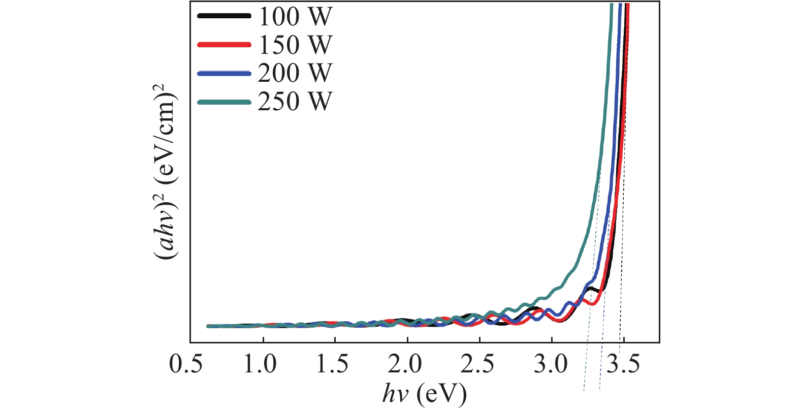
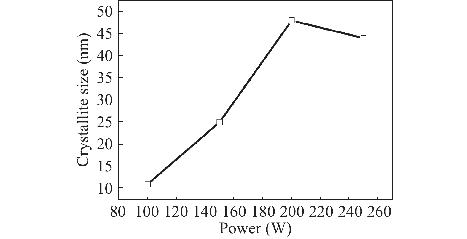
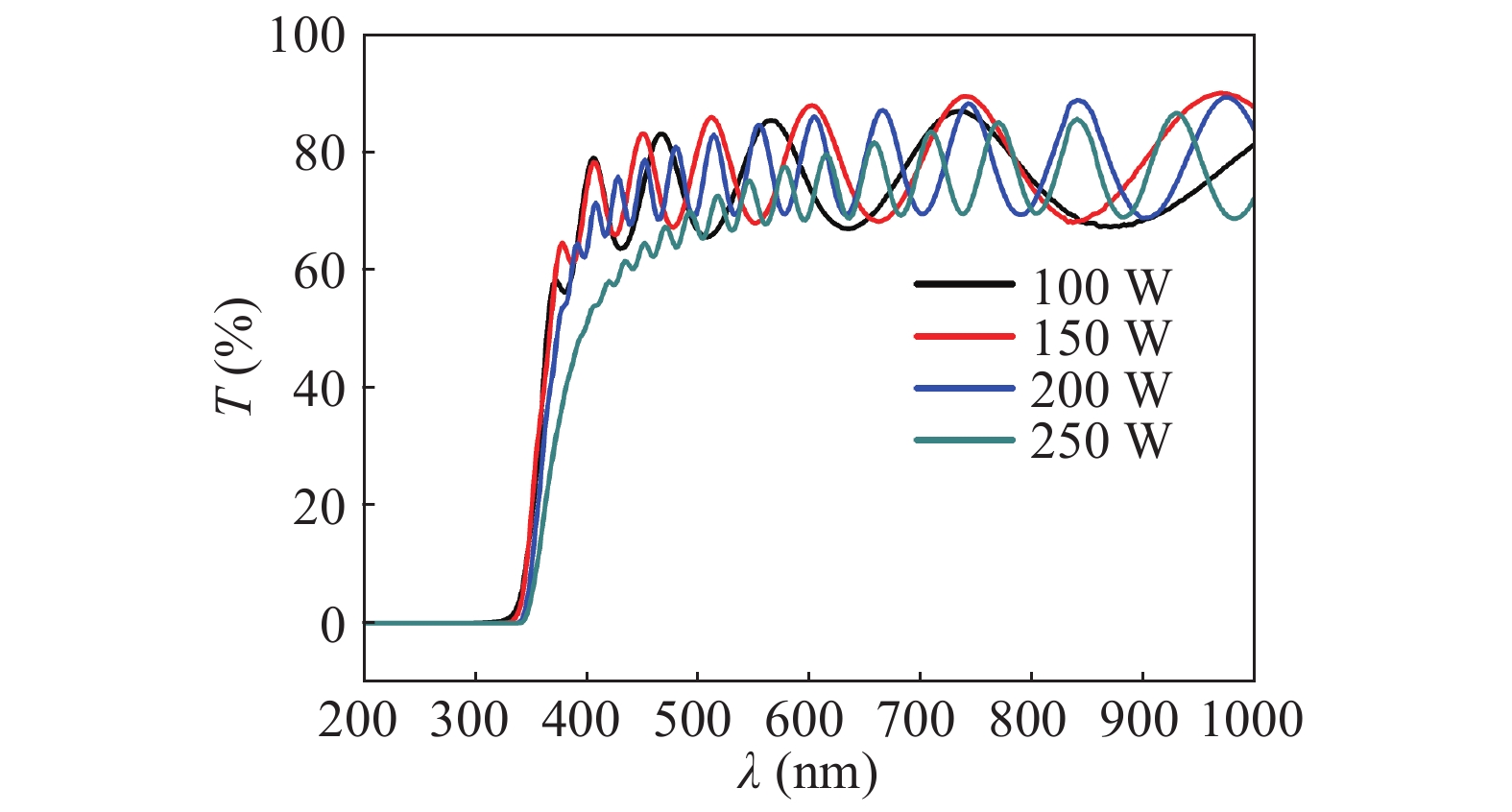
Abstract: Zinc sulphide (ZnS) thin films have grown on glass and Si substrates by reactive cathodic radio frequency (RF) sputtering. The RF power was varied in the range of 100 to 250 W, while the deposition time is set at 75 min. The optical, structural, and morphological properties of these thin films have been studied. The optical properties (mainly thickness, refractive index, absorption coefficient, and optical band gap) were investigated by optical transmittance measurements in the wavelength range of ultraviolet-visible-near infrared spectroscopy and spectroscopy infrared with Fourier transform. Fourier (FT-IR) and XRD analysis indicated that all sputtering ZnS films had a single-phase with a preferred orientation along the (111) plane of the zinc sphalerite phase (ZB). The crystallite size ranged from 11.5 to 48.5 nm with RF power getting a maximum of 200 W. UV–visible measurements exhibited that the ZnS film had more than 80% transmission in the visible wavelength region. In addition, it has been observed that the band gap energy of ZnS films is decreased slightly from 3.52 to 3.29 eV, and as the RF power is increased, the film thickness increases with the speed of deposit growth. Scanning electron microscopy observations revealed the types of smooth-surfaced films. The measurements (FT-IR) revealed at wave number 1118 and 465.02 cm−1 absorption bands corresponding to the symmetrical and asymmetric vibration of the Zn–S stretching mode. X-ray reflectometry measurements of ZnS films have shown that the density of the films is (3.9 g/cm3) close to that of solid ZnS.
Keywords: ZnS thin films by sputtered, RF-sputtering ZnS, ZnS buffer layer for solar cell
| [1] |
Bodke M, Khawal H, Gawai U, et al. Synthesis and characterization of chromium doped zinc sulfide nanoparticles. Open ACLib S, 2015, 2: 1549 doi: 10.4236/oalib.1101549
|
| [2] |
Chelvanathan P, Yusoff Y, Haque F, et al. Growth and characterization of RF-sputtered ZnS thin film deposited at various substrate temperatures for photovoltaic application. Appl Surf Sci, 2015, 334: 144 doi: 10.1016/j.apsusc.2014.08.155
|
| [3] |
Gode F. Annealing temperature effect on the structural, optical and electrical properties of ZnS thin films. Phys B, 2011, 406: 1659 doi: 10.1016/j.physb.2010.12.033
|
| [4] |
Zhong Z Y, Cho E S, Kwon S J. Characterization of the ZnS thin film buffer layer for Cu(In, Ga)Se2 solar cells deposited by chemical bath deposition process with different solution concentrations. Mater Chem Phys, 2012, 135: 292 doi: 10.1016/j.matchemphys.2012.03.090
|
| [5] |
Goudarzi A, Aval G M, Sahraei R, et al. Ammonia-free chemical bath deposition of nanocrystalline ZnS thin film buffer layer for solar cells. Thin Sold Flms, 2008, 516: 4957 doi: 10.1016/j.tsf.2007.09.051
|
| [6] |
Tec-Yam S, Rojas J, Rejón V, et al. High quality antire flective ZnS thin films prepared by chemical bath deposition. Mater Chem Phys, 2012, 136: 393 doi: 10.1016/j.matchemphys.2012.06.063
|
| [7] |
Wang H, Lu X, Zhao Y, et al. Preparation and characterization of ZnS: Cu/PVA composite nanofibers via electrospinning. Mater Sci Lett, 2006, 60: 2484 doi: 10.1016/j.matlet.2006.01.021
|
| [8] |
Ra S, Wook S, Sun D, et al. Effect of pH on the characteristics of nanocrystalline ZnS thin films prepared by CBD method in acidic medium. Cur Appl Phys, 2010, 10: 77 doi: 10.1016/j.cap.2010.02.052
|
| [9] |
Hwang D H, Ahn J H, Hui K N, et al. Structural and optical properties of ZnS thin films deposited by RF magnetron sputtering. Nanoscale Res Lett, 2012, 7: 26 doi: 10.1186/1556-276X-7-26
|
| [10] |
Ghribi F, El Mir L, Omri K, et al. Optik sputtered ZnS thin film from nanoparticles synthesized by hydrothermal route. Opt Int Light Electron Opt, 2016, 127: 3692 doi: 10.1016/j.ijleo.2016.01.022
|
| [11] |
Akhtar M S, Riaz S, Naseem S. Optical properties of sol-gel deposited ZnS thin films: spectroscopic ellipsometry. Mater Today, 2015, 2: 10 doi: 10.1016/j.matpr.2015.11.076
|
| [12] |
Zhang R, Wang B, Wei L. Influence of RF power on the structure of ZnS thin films grown by sulfurizing RF sputter deposited ZnO. Mater Chem Phys, 2008, 112: 561 doi: 10.1016/j.matchemphys.2008.05.089
|
| [13] |
El Khalfi A, Ech-chamikh E, Ijdiyaou Y, et al. Optical properties of amorphous silicon–carbon alloys (a-SixC1-x) deposited by RF co-sputtering. Arab Sci Eng, 2014, 39: 5776 doi: 10.1007/s13369-014-1134-3
|
| [14] |
Nkhaili L, Ali M A, Outzouriht A, et al. Effect of RF power on the structural and optical properties of RF-sputtered ZnO thin films. Eur Phys Appl Phys, 2014, 66(3): 30302 doi: 10.1051/epjap/2014140098
|
| [15] |
El Khalfi A, Ech-chamikh E, Ijdiyaou Y, et al. Infrared and Raman study of amorphous silicon carbide thin films deposited by radiofrequency co-sputtering. Spectrosc Lett, 2014, 41, 11: 396 doi: 10.1080/00387010.2013.840849
|
| [16] |
El kissani A, Nkhaili L, Outzourhit A. Synthesis, annealing, characterization and electronic properties of thin films of a quaternary semiconductor; copper zinc tin sulfide. Spectrosc Lett, 2016, 7010: 2289 doi: 10.1080/00387010.2016.1167086
|
| [17] |
Wook S, Agawane G L, Gil M. Preparation and characteristics of chemical bath deposited ZnS thin films: Effects of different complexing agents. Alloys Compd, 2012, 526: 30 doi: 10.1016/j.jallcom.2012.02.084
|
| [18] |
Pimpabute W S N, Burinprakhon T. Determination of optical constants and thickness of amorphous GaP thin film. Opt Appl, 2011, 41(1): 257
|
| [19] |
Shaaban E R, Yahia I S. Validity of Swanepoel's method for calculating the optical constants of thick films. Acta Phys Pol A, 2012, 121: 635 doi: 10.12693/APhysPolA.121.628
|
| [20] |
Lokhande C D, Lee E, Jung K, et al. Ammonia-free chemical bath method for deposition of microcrystalline cadmium selenide films. Mater Chem Phys, 2005, 91: 204 doi: 10.1016/j.matchemphys.2004.11.014
|
| [21] |
Deepa K, Preetha K C, Murali K V, et al. The effect of various complexing agents on the morphology and optoelectronic properties of chemically deposited ZnS thin films: A comparative study. Opt In Light Electron Opt, 2014, 125: 5732 doi: 10.1016/j.ijleo.2014.06.028
|
| [22] |
Rodríguez C A, Sandoval-paz M G, Cabello G, et al. Characterization of ZnS thin fi lms synthesized through a non-toxic precursors chemical bath. Mater Res Bull, 2014, 60: 321 doi: 10.1016/j.materresbull.2014.08.047
|
| [23] |
Ech-chamikh E, Essafti A, Youssef I. Une méthode simple et précise pour la détermination de l’épaisseur de couches ultraminces à partir des mesures de réflectométrie des rayons X. Africa Sci, 2006, 2: 262
|
| [24] |
Ghosh P K, Jana S, Nandy S, et al. Size-dependent optical and dielectric properties of nanocrystalline ZnS thin films synthesized via rf-magnetron sputtering technique. Mater Res Bull, 2007, 42: 514 doi: 10.1016/j.materresbull.2006.06.019
|
| [25] |
El khalfi A, Ech-chamikh E, Ijdiyaou Y, et al. Structural and optical properties of RF sputtered SixC1-x thin films. Glob Phys Chem, 2011, 2: 124
|
| [26] |
Salavati-niasari M, Ranjbar M, Ghanbari D. A rapid microwave route for the synthesis of ZnS nanoparticles. Nanostructure, 2012, 1: 235 doi: 10.7508/JNS.2011.03.007
|
| [27] |
Mote V D, Purushotham Y, Dole B N, et al. Structural, morphological and optical properties of Mn doped ZnS nanocrystals. Ceram Sci, 2013, 59: 619 doi: 10.1590/S0366-69132013000400019
|
| [28] |
Labiadh H, Lahbib K, Hidouri S, et al. Insight of ZnS nanoparticles contribution in different biological uses. Asian Pac Trop Med, 2016, 9(8): 757 doi: 10.1016/j.apjtm.2016.06.008
|
| [29] |
Mubashshir M, Farooqi H, Srivastava R K. Structural, optical and photoconductivity study of ZnS nanoparticles synthesized by a low temperature solid state reaction method. Mater Sci Semicond Proc, 2014, 20: 67 doi: 10.1016/j.mssp.2013.12.028
|
| [30] |
El Khalfi A, Ech-chamikh E, Ijdiyaou Y, et al. FTIR and Raman study of rapid thermal annealing and oxidation effects on structural properties of silicon-rich SixC1-x thin films deposited by RF co-sputtering. Vibr Spectrosc, 2017, 89: 48 doi: 10.1016/j.vibspec.2016.12.004
|
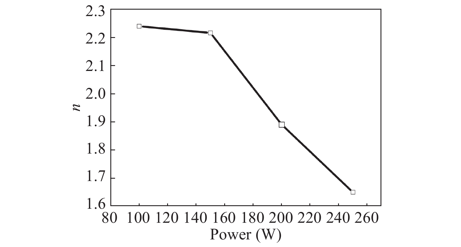
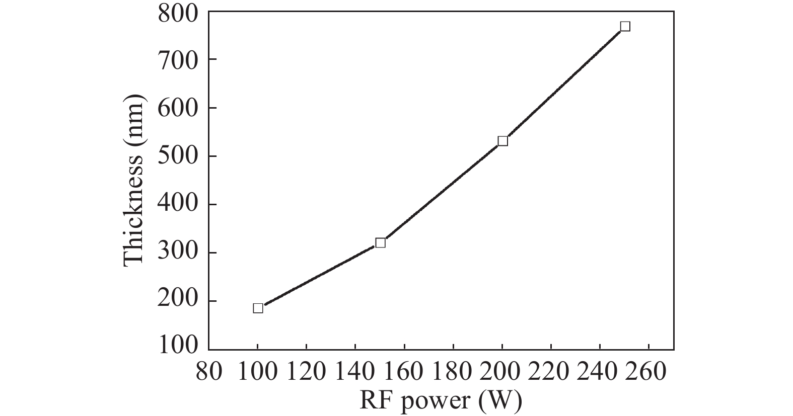
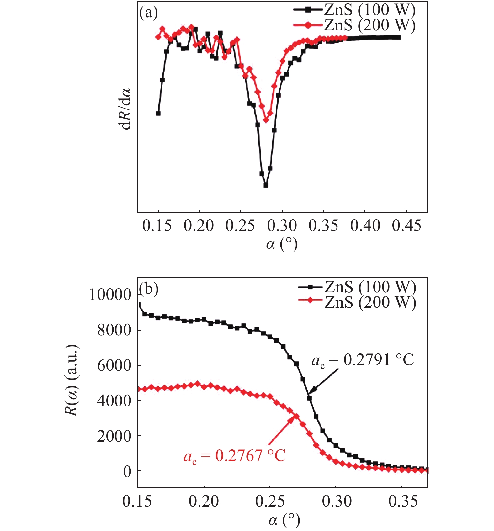
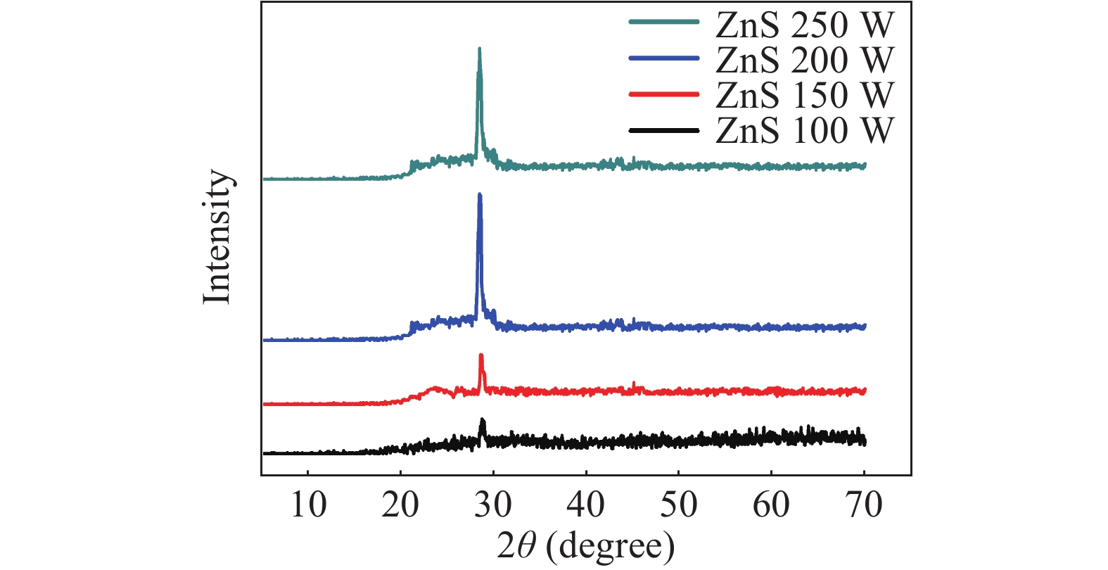
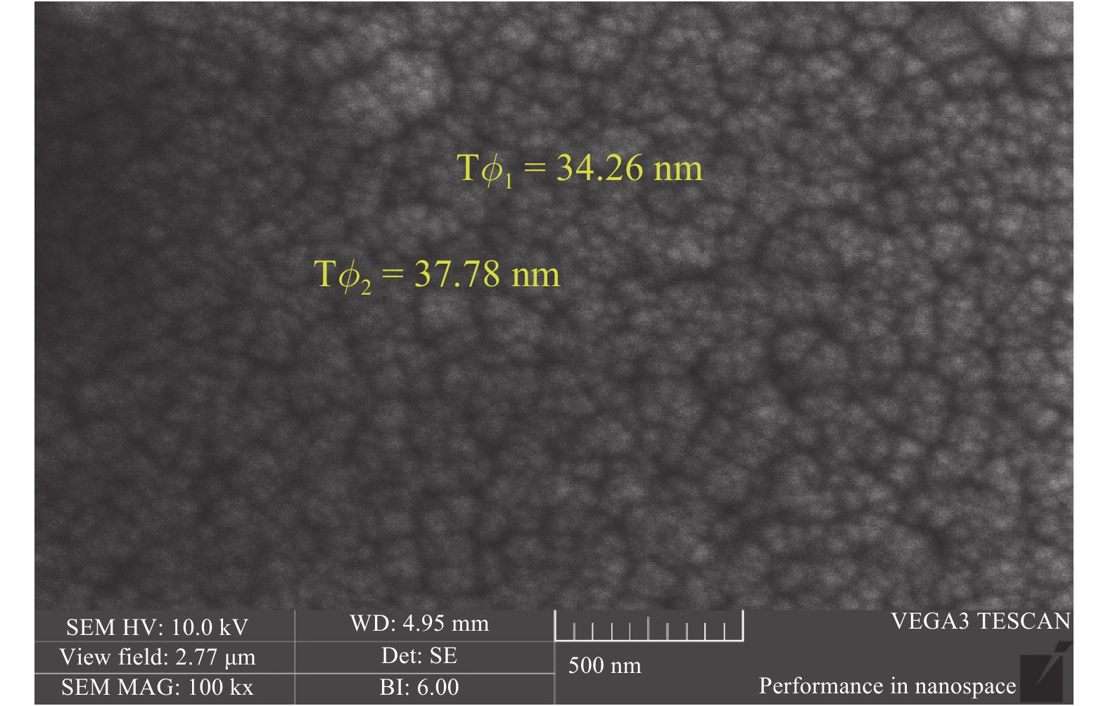
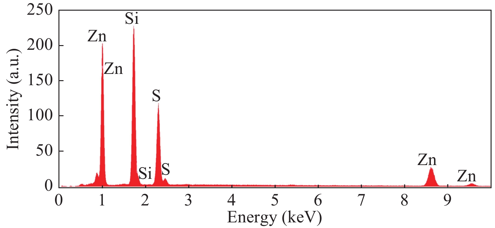
Table 1. The deposition parameters of the ZnS thin films.
| Parameter | Value |
| Deposition time | Fixed 75 min |
| RF-power (input-reflected) | Varied from 100 to 250 W |
| Target diameter | 10 cm |
| Target-substrate distance | 8 cm |
| Bombardment gas | Argon (Ar) |
| Gas pressure | 0.01 mbar |
| Substrates used | Glass, Si |
| Substrate temperature | 300 K |
 DownLoad: CSV
Table 2. Composition of the deposited ZnS films.
| Element | Weight (%) | Atomic (%) | Net Int. | Error (%) | K ratio |
| SiK | 35.98 | 48.60 | 1822.60 | 5.68 | 0.2229 |
| S K | 23.66 | 27.99 | 1019.15 | 5.69 | 0.1480 |
| ZnK | 40.35 | 23.41 | 429.43 | 3.28 | 0.3774 |
DownLoad: CSV
| [1] |
Bodke M, Khawal H, Gawai U, et al. Synthesis and characterization of chromium doped zinc sulfide nanoparticles. Open ACLib S, 2015, 2: 1549 doi: 10.4236/oalib.1101549
|
| [2] |
Chelvanathan P, Yusoff Y, Haque F, et al. Growth and characterization of RF-sputtered ZnS thin film deposited at various substrate temperatures for photovoltaic application. Appl Surf Sci, 2015, 334: 144 doi: 10.1016/j.apsusc.2014.08.155
|
| [3] |
Gode F. Annealing temperature effect on the structural, optical and electrical properties of ZnS thin films. Phys B, 2011, 406: 1659 doi: 10.1016/j.physb.2010.12.033
|
| [4] |
Zhong Z Y, Cho E S, Kwon S J. Characterization of the ZnS thin film buffer layer for Cu(In, Ga)Se2 solar cells deposited by chemical bath deposition process with different solution concentrations. Mater Chem Phys, 2012, 135: 292 doi: 10.1016/j.matchemphys.2012.03.090
|
| [5] |
Goudarzi A, Aval G M, Sahraei R, et al. Ammonia-free chemical bath deposition of nanocrystalline ZnS thin film buffer layer for solar cells. Thin Sold Flms, 2008, 516: 4957 doi: 10.1016/j.tsf.2007.09.051
|
| [6] |
Tec-Yam S, Rojas J, Rejón V, et al. High quality antire flective ZnS thin films prepared by chemical bath deposition. Mater Chem Phys, 2012, 136: 393 doi: 10.1016/j.matchemphys.2012.06.063
|
| [7] |
Wang H, Lu X, Zhao Y, et al. Preparation and characterization of ZnS: Cu/PVA composite nanofibers via electrospinning. Mater Sci Lett, 2006, 60: 2484 doi: 10.1016/j.matlet.2006.01.021
|
| [8] |
Ra S, Wook S, Sun D, et al. Effect of pH on the characteristics of nanocrystalline ZnS thin films prepared by CBD method in acidic medium. Cur Appl Phys, 2010, 10: 77 doi: 10.1016/j.cap.2010.02.052
|
| [9] |
Hwang D H, Ahn J H, Hui K N, et al. Structural and optical properties of ZnS thin films deposited by RF magnetron sputtering. Nanoscale Res Lett, 2012, 7: 26 doi: 10.1186/1556-276X-7-26
|
| [10] |
Ghribi F, El Mir L, Omri K, et al. Optik sputtered ZnS thin film from nanoparticles synthesized by hydrothermal route. Opt Int Light Electron Opt, 2016, 127: 3692 doi: 10.1016/j.ijleo.2016.01.022
|
| [11] |
Akhtar M S, Riaz S, Naseem S. Optical properties of sol-gel deposited ZnS thin films: spectroscopic ellipsometry. Mater Today, 2015, 2: 10 doi: 10.1016/j.matpr.2015.11.076
|
| [12] |
Zhang R, Wang B, Wei L. Influence of RF power on the structure of ZnS thin films grown by sulfurizing RF sputter deposited ZnO. Mater Chem Phys, 2008, 112: 561 doi: 10.1016/j.matchemphys.2008.05.089
|
| [13] |
El Khalfi A, Ech-chamikh E, Ijdiyaou Y, et al. Optical properties of amorphous silicon–carbon alloys (a-SixC1-x) deposited by RF co-sputtering. Arab Sci Eng, 2014, 39: 5776 doi: 10.1007/s13369-014-1134-3
|
| [14] |
Nkhaili L, Ali M A, Outzouriht A, et al. Effect of RF power on the structural and optical properties of RF-sputtered ZnO thin films. Eur Phys Appl Phys, 2014, 66(3): 30302 doi: 10.1051/epjap/2014140098
|
| [15] |
El Khalfi A, Ech-chamikh E, Ijdiyaou Y, et al. Infrared and Raman study of amorphous silicon carbide thin films deposited by radiofrequency co-sputtering. Spectrosc Lett, 2014, 41, 11: 396 doi: 10.1080/00387010.2013.840849
|
| [16] |
El kissani A, Nkhaili L, Outzourhit A. Synthesis, annealing, characterization and electronic properties of thin films of a quaternary semiconductor; copper zinc tin sulfide. Spectrosc Lett, 2016, 7010: 2289 doi: 10.1080/00387010.2016.1167086
|
| [17] |
Wook S, Agawane G L, Gil M. Preparation and characteristics of chemical bath deposited ZnS thin films: Effects of different complexing agents. Alloys Compd, 2012, 526: 30 doi: 10.1016/j.jallcom.2012.02.084
|
| [18] |
Pimpabute W S N, Burinprakhon T. Determination of optical constants and thickness of amorphous GaP thin film. Opt Appl, 2011, 41(1): 257
|
| [19] |
Shaaban E R, Yahia I S. Validity of Swanepoel's method for calculating the optical constants of thick films. Acta Phys Pol A, 2012, 121: 635 doi: 10.12693/APhysPolA.121.628
|
| [20] |
Lokhande C D, Lee E, Jung K, et al. Ammonia-free chemical bath method for deposition of microcrystalline cadmium selenide films. Mater Chem Phys, 2005, 91: 204 doi: 10.1016/j.matchemphys.2004.11.014
|
| [21] |
Deepa K, Preetha K C, Murali K V, et al. The effect of various complexing agents on the morphology and optoelectronic properties of chemically deposited ZnS thin films: A comparative study. Opt In Light Electron Opt, 2014, 125: 5732 doi: 10.1016/j.ijleo.2014.06.028
|
| [22] |
Rodríguez C A, Sandoval-paz M G, Cabello G, et al. Characterization of ZnS thin fi lms synthesized through a non-toxic precursors chemical bath. Mater Res Bull, 2014, 60: 321 doi: 10.1016/j.materresbull.2014.08.047
|
| [23] |
Ech-chamikh E, Essafti A, Youssef I. Une méthode simple et précise pour la détermination de l’épaisseur de couches ultraminces à partir des mesures de réflectométrie des rayons X. Africa Sci, 2006, 2: 262
|
| [24] |
Ghosh P K, Jana S, Nandy S, et al. Size-dependent optical and dielectric properties of nanocrystalline ZnS thin films synthesized via rf-magnetron sputtering technique. Mater Res Bull, 2007, 42: 514 doi: 10.1016/j.materresbull.2006.06.019
|
| [25] |
El khalfi A, Ech-chamikh E, Ijdiyaou Y, et al. Structural and optical properties of RF sputtered SixC1-x thin films. Glob Phys Chem, 2011, 2: 124
|
| [26] |
Salavati-niasari M, Ranjbar M, Ghanbari D. A rapid microwave route for the synthesis of ZnS nanoparticles. Nanostructure, 2012, 1: 235 doi: 10.7508/JNS.2011.03.007
|
| [27] |
Mote V D, Purushotham Y, Dole B N, et al. Structural, morphological and optical properties of Mn doped ZnS nanocrystals. Ceram Sci, 2013, 59: 619 doi: 10.1590/S0366-69132013000400019
|
| [28] |
Labiadh H, Lahbib K, Hidouri S, et al. Insight of ZnS nanoparticles contribution in different biological uses. Asian Pac Trop Med, 2016, 9(8): 757 doi: 10.1016/j.apjtm.2016.06.008
|
| [29] |
Mubashshir M, Farooqi H, Srivastava R K. Structural, optical and photoconductivity study of ZnS nanoparticles synthesized by a low temperature solid state reaction method. Mater Sci Semicond Proc, 2014, 20: 67 doi: 10.1016/j.mssp.2013.12.028
|
| [30] |
El Khalfi A, Ech-chamikh E, Ijdiyaou Y, et al. FTIR and Raman study of rapid thermal annealing and oxidation effects on structural properties of silicon-rich SixC1-x thin films deposited by RF co-sputtering. Vibr Spectrosc, 2017, 89: 48 doi: 10.1016/j.vibspec.2016.12.004
|


Article views: 5383 Times PDF downloads: 100 Times Cited by: 0 Times
Received: 12 April 2018 Revised: 30 May 2018 Online: Accepted Manuscript: 23 July 2018Uncorrected proof: 23 July 2018Corrected proof: 01 November 2018Published: 13 December 2018
| Citation: |
C. M. Samba Vall, M. Chaik, H. Ait Dads, H. El Aakib, M. Elyaagoubi, M. Aggour, A. Outzourhit. Effect of RF power on the structural and optical properties of ZnS thin films prepared by RF-sputtering[J]. Journal of Semiconductors, 2018, 39(12): 123001. doi: 10.1088/1674-4926/39/12/123001
****
C M S Vall, M Chaik, H A Dads, H El Aakib, M Elyaagoubi, M Aggour, A Outzourhit, Effect of RF power on the structural and optical properties of ZnS thin films prepared by RF-sputtering[J]. J. Semicond., 2018, 39(12): 123001. doi: 10.1088/1674-4926/39/12/123001.

|
| [1] |
Bodke M, Khawal H, Gawai U, et al. Synthesis and characterization of chromium doped zinc sulfide nanoparticles. Open ACLib S, 2015, 2: 1549 doi: 10.4236/oalib.1101549
|
| [2] |
Chelvanathan P, Yusoff Y, Haque F, et al. Growth and characterization of RF-sputtered ZnS thin film deposited at various substrate temperatures for photovoltaic application. Appl Surf Sci, 2015, 334: 144 doi: 10.1016/j.apsusc.2014.08.155
|
| [3] |
Gode F. Annealing temperature effect on the structural, optical and electrical properties of ZnS thin films. Phys B, 2011, 406: 1659 doi: 10.1016/j.physb.2010.12.033
|
| [4] |
Zhong Z Y, Cho E S, Kwon S J. Characterization of the ZnS thin film buffer layer for Cu(In, Ga)Se2 solar cells deposited by chemical bath deposition process with different solution concentrations. Mater Chem Phys, 2012, 135: 292 doi: 10.1016/j.matchemphys.2012.03.090
|
| [5] |
Goudarzi A, Aval G M, Sahraei R, et al. Ammonia-free chemical bath deposition of nanocrystalline ZnS thin film buffer layer for solar cells. Thin Sold Flms, 2008, 516: 4957 doi: 10.1016/j.tsf.2007.09.051
|
| [6] |
Tec-Yam S, Rojas J, Rejón V, et al. High quality antire flective ZnS thin films prepared by chemical bath deposition. Mater Chem Phys, 2012, 136: 393 doi: 10.1016/j.matchemphys.2012.06.063
|
| [7] |
Wang H, Lu X, Zhao Y, et al. Preparation and characterization of ZnS: Cu/PVA composite nanofibers via electrospinning. Mater Sci Lett, 2006, 60: 2484 doi: 10.1016/j.matlet.2006.01.021
|
| [8] |
Ra S, Wook S, Sun D, et al. Effect of pH on the characteristics of nanocrystalline ZnS thin films prepared by CBD method in acidic medium. Cur Appl Phys, 2010, 10: 77 doi: 10.1016/j.cap.2010.02.052
|
| [9] |
Hwang D H, Ahn J H, Hui K N, et al. Structural and optical properties of ZnS thin films deposited by RF magnetron sputtering. Nanoscale Res Lett, 2012, 7: 26 doi: 10.1186/1556-276X-7-26
|
| [10] |
Ghribi F, El Mir L, Omri K, et al. Optik sputtered ZnS thin film from nanoparticles synthesized by hydrothermal route. Opt Int Light Electron Opt, 2016, 127: 3692 doi: 10.1016/j.ijleo.2016.01.022
|
| [11] |
Akhtar M S, Riaz S, Naseem S. Optical properties of sol-gel deposited ZnS thin films: spectroscopic ellipsometry. Mater Today, 2015, 2: 10 doi: 10.1016/j.matpr.2015.11.076
|
| [12] |
Zhang R, Wang B, Wei L. Influence of RF power on the structure of ZnS thin films grown by sulfurizing RF sputter deposited ZnO. Mater Chem Phys, 2008, 112: 561 doi: 10.1016/j.matchemphys.2008.05.089
|
| [13] |
El Khalfi A, Ech-chamikh E, Ijdiyaou Y, et al. Optical properties of amorphous silicon–carbon alloys (a-SixC1-x) deposited by RF co-sputtering. Arab Sci Eng, 2014, 39: 5776 doi: 10.1007/s13369-014-1134-3
|
| [14] |
Nkhaili L, Ali M A, Outzouriht A, et al. Effect of RF power on the structural and optical properties of RF-sputtered ZnO thin films. Eur Phys Appl Phys, 2014, 66(3): 30302 doi: 10.1051/epjap/2014140098
|
| [15] |
El Khalfi A, Ech-chamikh E, Ijdiyaou Y, et al. Infrared and Raman study of amorphous silicon carbide thin films deposited by radiofrequency co-sputtering. Spectrosc Lett, 2014, 41, 11: 396 doi: 10.1080/00387010.2013.840849
|
| [16] |
El kissani A, Nkhaili L, Outzourhit A. Synthesis, annealing, characterization and electronic properties of thin films of a quaternary semiconductor; copper zinc tin sulfide. Spectrosc Lett, 2016, 7010: 2289 doi: 10.1080/00387010.2016.1167086
|
| [17] |
Wook S, Agawane G L, Gil M. Preparation and characteristics of chemical bath deposited ZnS thin films: Effects of different complexing agents. Alloys Compd, 2012, 526: 30 doi: 10.1016/j.jallcom.2012.02.084
|
| [18] |
Pimpabute W S N, Burinprakhon T. Determination of optical constants and thickness of amorphous GaP thin film. Opt Appl, 2011, 41(1): 257
|
| [19] |
Shaaban E R, Yahia I S. Validity of Swanepoel's method for calculating the optical constants of thick films. Acta Phys Pol A, 2012, 121: 635 doi: 10.12693/APhysPolA.121.628
|
| [20] |
Lokhande C D, Lee E, Jung K, et al. Ammonia-free chemical bath method for deposition of microcrystalline cadmium selenide films. Mater Chem Phys, 2005, 91: 204 doi: 10.1016/j.matchemphys.2004.11.014
|
| [21] |
Deepa K, Preetha K C, Murali K V, et al. The effect of various complexing agents on the morphology and optoelectronic properties of chemically deposited ZnS thin films: A comparative study. Opt In Light Electron Opt, 2014, 125: 5732 doi: 10.1016/j.ijleo.2014.06.028
|
| [22] |
Rodríguez C A, Sandoval-paz M G, Cabello G, et al. Characterization of ZnS thin fi lms synthesized through a non-toxic precursors chemical bath. Mater Res Bull, 2014, 60: 321 doi: 10.1016/j.materresbull.2014.08.047
|
| [23] |
Ech-chamikh E, Essafti A, Youssef I. Une méthode simple et précise pour la détermination de l’épaisseur de couches ultraminces à partir des mesures de réflectométrie des rayons X. Africa Sci, 2006, 2: 262
|
| [24] |
Ghosh P K, Jana S, Nandy S, et al. Size-dependent optical and dielectric properties of nanocrystalline ZnS thin films synthesized via rf-magnetron sputtering technique. Mater Res Bull, 2007, 42: 514 doi: 10.1016/j.materresbull.2006.06.019
|
| [25] |
El khalfi A, Ech-chamikh E, Ijdiyaou Y, et al. Structural and optical properties of RF sputtered SixC1-x thin films. Glob Phys Chem, 2011, 2: 124
|
| [26] |
Salavati-niasari M, Ranjbar M, Ghanbari D. A rapid microwave route for the synthesis of ZnS nanoparticles. Nanostructure, 2012, 1: 235 doi: 10.7508/JNS.2011.03.007
|
| [27] |
Mote V D, Purushotham Y, Dole B N, et al. Structural, morphological and optical properties of Mn doped ZnS nanocrystals. Ceram Sci, 2013, 59: 619 doi: 10.1590/S0366-69132013000400019
|
| [28] |
Labiadh H, Lahbib K, Hidouri S, et al. Insight of ZnS nanoparticles contribution in different biological uses. Asian Pac Trop Med, 2016, 9(8): 757 doi: 10.1016/j.apjtm.2016.06.008
|
| [29] |
Mubashshir M, Farooqi H, Srivastava R K. Structural, optical and photoconductivity study of ZnS nanoparticles synthesized by a low temperature solid state reaction method. Mater Sci Semicond Proc, 2014, 20: 67 doi: 10.1016/j.mssp.2013.12.028
|
| [30] |
El Khalfi A, Ech-chamikh E, Ijdiyaou Y, et al. FTIR and Raman study of rapid thermal annealing and oxidation effects on structural properties of silicon-rich SixC1-x thin films deposited by RF co-sputtering. Vibr Spectrosc, 2017, 89: 48 doi: 10.1016/j.vibspec.2016.12.004
|

 WeChat ID
Journal of Semiconductors © 2017 All Rights Reserved 京ICP备05085259号-2