J. Semicond. > 2018, Volume 39 > Issue 2 > 024004

SEMICONDUCTOR DEVICES

Reliability analysis of magnetic logic interconnect wire subjected to magnet edge imperfections

Bin Zhang1, , Xiaokuo Yang1, , Jiahao Liu1, Weiwei Li1, 2 and Jie Xu1

+ Author Affiliations

 Corresponding author: Bin Zhang, Email: kgdzhangbin@163.com; Xiaokuo Yang, yangxk0123@163.com

DOI: 10.1088/1674-4926/39/2/024004

PDF

Turn off MathJax

Abstract: Nanomagnet logic (NML) devices have been proposed as one of the best candidates for the next generation of integrated circuits thanks to its substantial advantages of nonvolatility, radiation hardening and potentially low power. In this article, errors of nanomagnetic interconnect wire subjected to magnet edge imperfections have been evaluated for the purpose of reliable logic propagation. The missing corner defects of nanomagnet in the wire are modeled with a triangle, and the interconnect fabricated with various magnetic materials is thoroughly investigated by micromagnetic simulations under different corner defect amplitudes and device spacings. The results show that as the defect amplitude increases, the success rate of logic propagation in the interconnect decreases. More results show that from the interconnect wire fabricated with materials, iron demonstrates the best defect tolerance ability among three representative and frequently used NML materials, also logic transmission errors can be mitigated by adjusting spacing between nanomagnets. These findings can provide key technical guides for designing reliable interconnects.

Key words: nanomagnet logic devicedefectinterconnectreliability

Metal halide perovskites have made rapid progress in photonic and optoelectronic applications since the first report of solid-state perovskite solar cells in 2012[1]. Perovskites feature superior luminescence properties beneficial for the application in light emitting diodes (LEDs), such as high photoluminescence quantum yields (PLQYs), narrow emission, and tunable bandgaps[2, 3]. Low-cost perovskite LEDs (PeLEDs) have attracted interests, causing fast enhancement of their performances, and demonstrating great potential in next-generation lighting and display applications.

Quasi-2D perovskites represent an important category of perovskites, with great success in light emission applications due to their unique and excellent optoelectronic properties. It is characterized through a sandwich structure that PbX6 octahedra sheets are packaged by large ammonium cations, forming a layered either Ruddlesden-Popper (RP) phase with formula of L2Sn–1PbnX3n+1, or Dion-Jacobson (DJ) phase with formula of LSn–1PbnX3n+1, where L is monovalent or divalent ammonium cation, S is small cation, X is halide anion, and n is the order of quasi-2D perovskite (the number of stacked PbX6 sheets). Quasi-2D perovskites with reduced dimension can construct self-organized multiple quantum-wells to induce both dielectric- and quantum-confinement effects, thus improving exciton binding energy over several hundred meV and enabling PLQYs up to 100%[4-6]. The emission behavior of quasi-2D perovskites is also determined by exciton recombination kinetics, and the management of singlet and triplet excitons in quasi-2D perovskites is fundamental for designing efficient PeLEDs and laser gain media[7]. In addition, there are efficient energy funnels from low-n value to high-n value domains in mixed-phase quasi-2D perovskite emitting layers, leading to accumulated excitons in the recombination centers, which is beneficial for high radiative recombination efficiency and PLQY even at low pump power densities[8].

Efforts have been devoted to designing and fabricating high-quality quasi-2D perovskite films for laser and LED applications. Qin et al. first reported stable room-temperature continuous photoinduced perovskite laser[9]. Meanwhile, extensive works on quasi-2D perovskites have been performed to improve the performance of PeLEDs, demonstrating highly efficient green devices with over 25% EQE, red and near-infrared devices over 20%, and blue devices over 10%, respectively[10-12]. Domain distribution controlling and defect passivation in quasi-2D perovskite emitting layers are the most effective strategies for quasi-2D PeLEDs.

Quasi-2D perovskite films feature a mixed phase rather than a single phase because the formation energies for different phases are similar. The solubility difference of precursor components and steric hindrance difference between cations cause a wide domain distribution, which may cause several problems. First, low-n value (n = 1 and 2) domains with reduced crystal size accompany with more traps, resulting in serious trap-induced nonradiative recombination. Second, though the energy transfer from low-n domains to adjacent high-n domains is faster than trapping, the energy loss still inevitably exists. At last, the higher-n (n > 10) domains tend to form free carriers and make nonradiative recombination, which also yields modest PLQY. It is important to narrow the distribution to avoid nonradiative recombination.

Zhang et al. made quasi-2D perovskite films with a narrow domain distribution by using two additives, ZrO2 nanoparticles (NPs) and cryptand[13]. ZrO2 NPs promote synchronous crystallization by facilitating the interaction between solvent and antisolvent, and cryptand complexing with Pb2+ retards the crystallization of high-n domains by forming an intermediate state, thus enhancing EQE of green PeLED from 16% to 21%. Narrowing domain distribution can also improve emission color purity and achieve spectra-stable blue devices. Yantara et al. reported that composition engineering through prudent selection of the cations coupled with rapid nucleation can result in a narrow domain distribution[14] (Fig. 1(b)). Methanesulfonate was used to reconstruct quasi-2D perovskite, yielding green PeLEDs with >20% EQE (Fig. 1(c))[15]. Ma et al. used a bifunctional additive, tris(4-fluorophenyl)phosphine oxide (TFPPO), to prepare quasi-2D perovskites with a monodispersed domain distribution[10]. The fluorine atoms make hydrogen bonding with organic cations, controlling their diffusion and suppressing the formation of low-n domains (Fig. 1(d)), and phosphine oxide moiety passivates grain boundaries via coordinating with the unsaturated sites. Green PeLEDs with an EQE of 25.6% were obtained.

Figure  1.  (Color online) (a) Competition between radiative recombination and nonradiative recombination for domains with different n. Reproduced with permission[13], Copyright 2021, Wiley. (b) The strategy to form intermediate domains for emissive quasi-2D perovskite films. Reproduced with permission[14], Copyright 2020, American Chemical Society. (c) Effect of MeS on domain distribution in quasi-2D perovskite films. Reproduced with permission[15], Copyright 2021, Springer Nature. (d) Domain distribution controlling by using TFPPO. Reproduced with permission[10], Copyright 2021, Springer Nature.

Inevitable defects and traps can easily form in polycrystalline perovskite films during crystallization in solution-processing methods. Compared with 3D perovskites, quasi-2D perovskites with reduced crystal size have higher defect densities. The charged defects can act as nonradiative recombination centers to decrease emission efficiency.

Halide anion vacancies in quasi-2D perovskites are usually shallow-level defects (at least for Br- or I-containing perovskites), which are not detrimental to device performance. Defects with deep trap states such as interstitial or anti-site defects are almost absent in perovskites since they have high formation energies. Coordination-unsaturated Pb ion can act as nonradiative recombination centers, which should be treated seriously during passivation[16, 17]. Understanding the effect of defects on device performance, and developing passivation strategies are critical for enhancing the performance of quasi-2D PeLEDs.

Passivators with X=O bond (X: P, C, S or other atoms) are effective to coordinate with Pb defects. Among them, the P=O:Pb dative bond showed a strong binding energy of 1.1 eV, avoiding nonradiative recombination caused by Pb defects[4]. Passivation agent with P=O such as trioctylphosphine oxide, triphenylphosphine oxide, as well as their derivatives all enhanced PLQY of quasi-2D perovskite films[10]. Meanwhile, Pb defects exposed at the edge of quasi-2D perovskite can also cause the instability. Photogenerated and electrically-injected carriers diffuse to perovskite edges and produce superoxide, causing rapid photodegradation (Fig. 2(a)). Quan et al. reported an edge-stabilization strategy of passivating exposed Pb defects by P=O bonds, which improved EQE and stability of quasi-2D PeLEDs[4]. C=O and C–O–C bonds also demonstrate outstanding Pb-defect passivation ability[6, 18]. Liu et al. developed a dual-additive strategy to prepare quasi-2D perovskite films with low defect density and high environmental stability by using 18-crown-6 and poly(ethylene glycol) methyl ether acrylate (MPEG-MAA) as additives (Fig. 2(b))[18]. The EQE of green PeLEDs reached 28.1%. 1-butyl-3-methylimidazolium tetrafluoroborate (BMIMBF4) ionic liquid can also passivate Pb defects[19]. Spontaneously formed targeted distribution of the ionic additive well matches the defect site distribution (Fig. 2(c)). Novel passivators with more functions have been explored. Phosphonate-triphenylphosphine oxide with dual roles of passivating defects and enhancing carrier radiative recombination boosted EQE over 25%[20]. Phosphine oxide can enhance PLQY by passivating Pb defects, and phosphonate with strong electron affinity can accelerate carrier radiative recombination by capturing injected electrons (Fig. 2(d)). Defect passivation plays critical role to realize highly efficient PeLEDs.

Figure  2.  (Color online) (a) Degradation mechanisms and edge-stabilization strategy via P=O bonds. Reproduced with permission[4], Copyright 2020, Springer Nature. (b) Schematic illustration of crystal structure change and defect passivation by crown and MPEG-MAA. Reproduced with permission[18], Copyright 2021, Wiley. (c) Passivation mechanism of ionic liquid additive with C=N bond. Reproduced with permission[19], Copyright 2021, American Chemical Society. (d) PE-TPPO-modified PeLED. Reproduced with permission[20], Copyright 2022, Wiley.

In short, domain controlling and defect passivation are effective approaches to enhance EQE for quasi-2D PeLEDs. There are still challenges, such as highly efficient pure red and blue emission, long-term operation stability, and environmental safety.

We thank the National Natural Science Foundation of China (22075277, 22109156) and the China Postdoctoral Science Foundation (2021M703129) for financial support. L. Ding thanks the National Key Research and Development Program of China (2017YFA0206600) and the National Natural Science Foundation of China (51773045, 21772030, 51922032, and 21961160720) for financial support.


[1]
Bernstein K, Cavin III R K, Porod W, et al. Device and architecture outlook for beyond CMOS switches. Proc IEEE, 2010, 98(12): 2169 doi: 10.1109/JPROC.2010.2066530
[2]
Tóth G, Lent C S. Quantum computing with quantum-dot cellular automata. Phys Rev A, 2001, 63(5): 052315 doi: 10.1103/PhysRevA.63.052315
[3]
Colci M, Johnson M. Dipolar coupling between nanopillar spin valves and magnetic quantum cellular automata arrays. IEEE Trans Nanotechnol, 2013, 12(5): 824 doi: 10.1109/TNANO.2013.2275033
[4]
Imre A, Csaba G, Ji L, et al. Majority logic gate for magnetic quantum-dot cellular automata. Science, 2006, 311(5758): 205 doi: 10.1126/science.1120506
[5]
Yang X K, Cai L, Zhang B, et al. Micromagnetic simulation of exploratory magnetic logic device with missing corner defect. J Magn Magn Mater, 2015(11): 391 doi: 10.1016/j.jmmm.2015.06.068
[6]
Allwood D A, Xiong G, Faulkner C C, et al. Magnetic domain-wall logic. Science, 2005, 309(5741): 1688 doi: 10.1126/science.1108813
[7]
Suh D I, Kil J P, Kim K W, et al. A single magnetic tunnel junction representing the basic logic functions-NAND, NOR, and IMP. IEEE Electron Device Letters, 2015, 36(4): 402 doi: 10.1109/LED.2015.2406881
[8]
Fong X, Kim Y, Yogendra K, et al. Spin-transfer torque devices for logic and memory: prospects and perspectives. IEEE Trans Comput-Aid Des Integr Circuits Syst, 2016, 35(1): 1 doi: 10.1109/TCAD.2015.2481793
[9]
Hu L, Hesjedal T. Micromagnetic investigation of the S-state reconfigurable logic element. IEEE Trans Magnet, 2012, 48(7): 2103 doi: 10.1109/TMAG.2012.2183607
[10]
Imtaar M A, Yadav A, Epping A, et al. Nanomagnet fabrication using nanoimprint lithography and electrodeposition. IEEE Trans Nanotechnol, 2013, 12(4): 547 doi: 10.1109/TNANO.2013.2257833
[11]
Yang X K, Cai L, Wang S Z, et al. Reliability and performance evaluation of QCA devices with rotation cell defect. IEEE Trans Nanotechnol, 2012, 11(9): 1009 doi: 10.1109/TNANO.2012.2211613
[12]
Niemier M, Varga E, Bernstein G H, et al. Shape engineering for controlled switching with nanomagnet logic. IEEE Trans Nanotechnol, 2012, 11(2): 220 doi: 10.1109/TNANO.2010.2056697
[13]
Shah F A, Sankar V K, Li P, et al. Compensation of orange-peel coupling effect in magnetic tunnel junction free layer via shape engineering for nanomagnet logic applications. J Appl Phys, 2014, 115(17): 17B902 doi: 10.1063/1.4863935
[14]
Spedalieri F M, Jacob A P, Nikonov D E, et al. Performance of magnetic quantum cellular automata and limitations due to thermal noise. IEEE Trans Nanotechnol, 2011, 10(3): 537 doi: 10.1109/TNANO.2010.2050597
[15]
Alam M T, Kurtz S J, Siddiq M. On-chip clocking of nanomagnet logic lines and gates. IEEE Trans Nanotechnol, 2012, 11(2): 273 doi: 10.1109/TNANO.2011.2169983
[16]
Chunsheng E, Rantschler J, Khizroev S, et al. Micromagnetics of signal propagation in magnetic cellular logic data channels. J Appl Phys, 2008, 104(5): 054311 doi: 10.1063/1.2975836
[17]
Donahue M J, Porter D G. OOMMF user's guide. Version 1.0. Interagency Report NISTIR 6376, National Institute of Standards and Technology (NIST), Gaithersburg, MD
[18]
Yang X K, Cai L, Wang J H, et al. Experimental study of magnetic quantum-dot cellular automata function arrays. Acta Phys Sin, 2012, 61(4): 047502
[19]
Kumari A, Bhanja S. Landauer clocking for magnetic cellular automata (MCA) arrays. IEEE Trans Very Large Scale Integr Syst, 2011, 19(4): 714 doi: 10.1109/TVLSI.2009.2036627
[20]
D’Souza N, Fashami M S, Bandyopadhyay S, et al. Experimental clocking of nanomagnets with strain for ultralow power boolean logic. Nano Lett, 2016, 16(2): 1069 doi: 10.1021/acs.nanolett.5b04205
[21]
Gross L, Schlittler R R, Meyer G, et al. Magnetologic devices fabricated by nanostencil lithography. Nanotechnology, 2010, 21(32): 325301 doi: 10.1088/0957-4484/21/32/325301
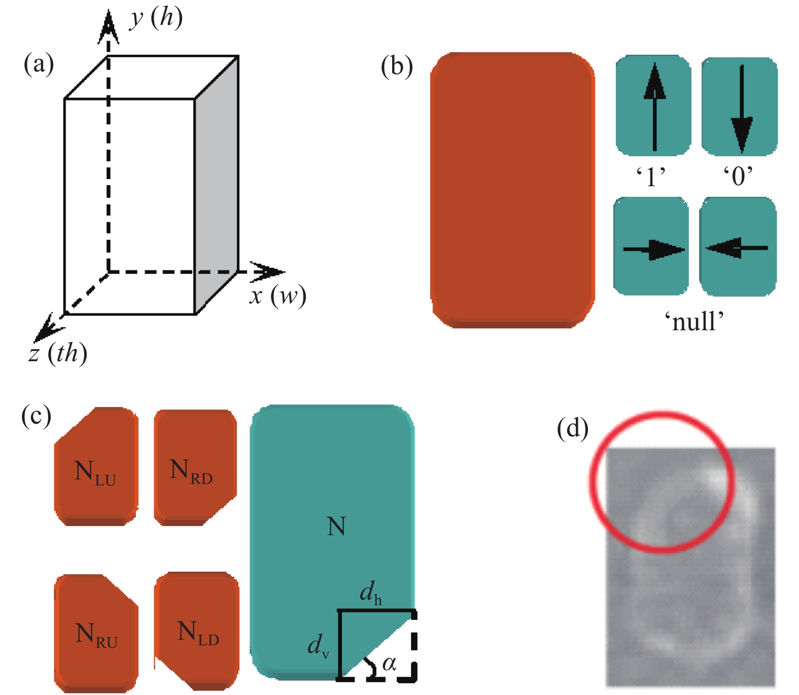
Fig. 1.  (Color online) The NML device and edge imperfection defect description. (a) Three dimension model of NML device. (b) The definition of NML logic state. (c) Edge imperfection defect modeling and four kinds of defects. (d) The scanning electron microscopy (SEM) image of defective nanomagnet.

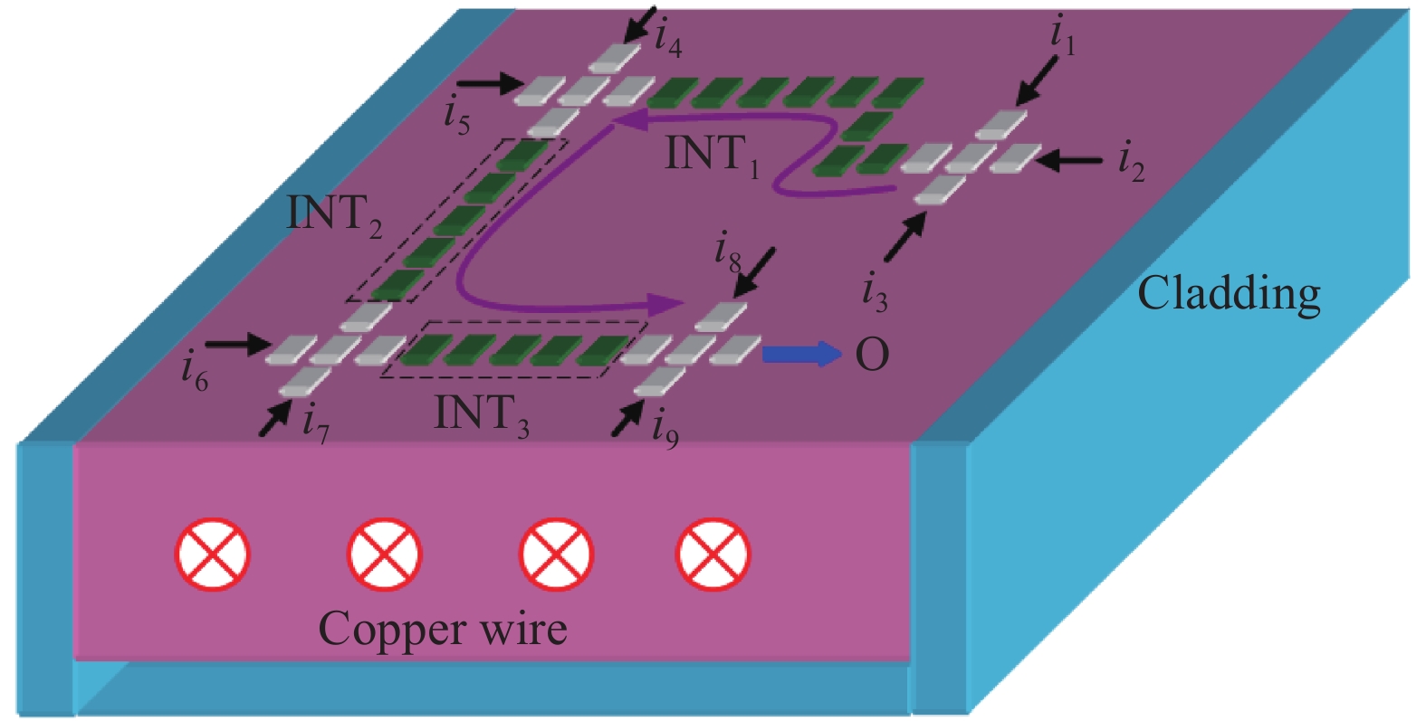
Fig. 2.  (Color online) An on-chip NML circuit layout containing several interconnect wires.

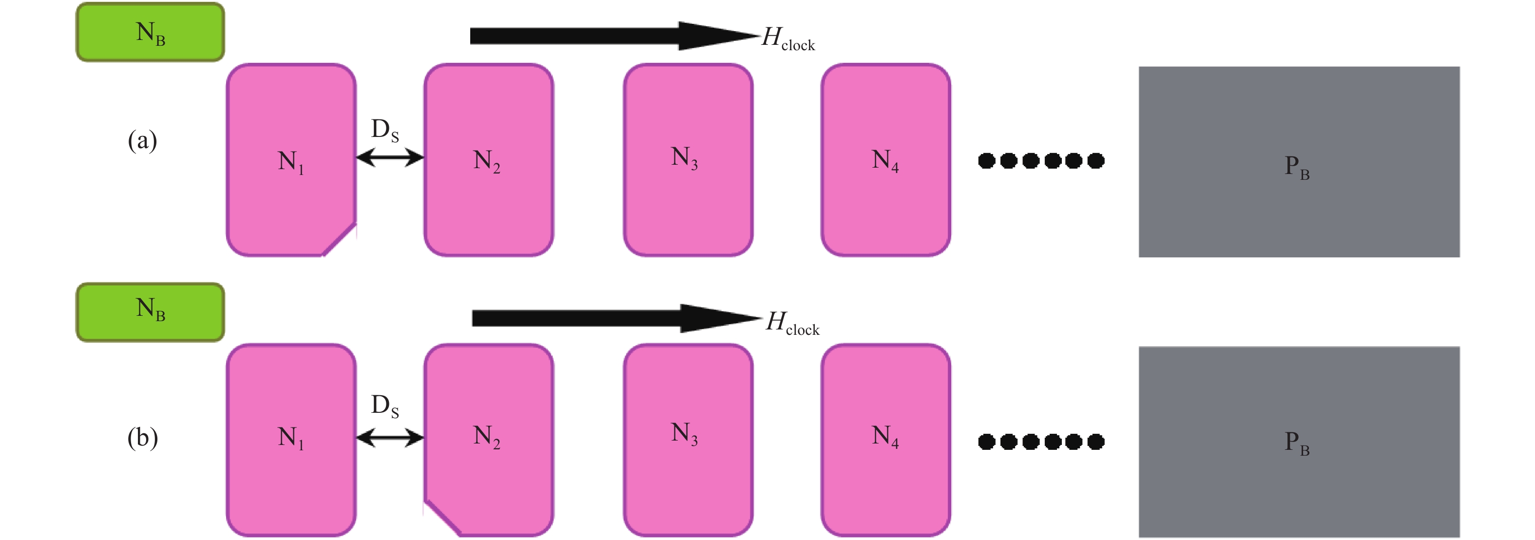
Fig. 3.  The NML interconnect wire containing one defective nanomagnet. (a) The NLU or NRD-type defective nanomagnet interconnect wire. (b) The NRU or NLD-type defective nanomagnet interconnect wire.

Fig. 4.  (Color online) Simulation results of interconnect wire shown in Fig. 3. (a) Tolerable edge missing amplitude of different nanomagnet. (b) The initial magnetization with the application of Hclock. (c) The final magnetization after evolvement.

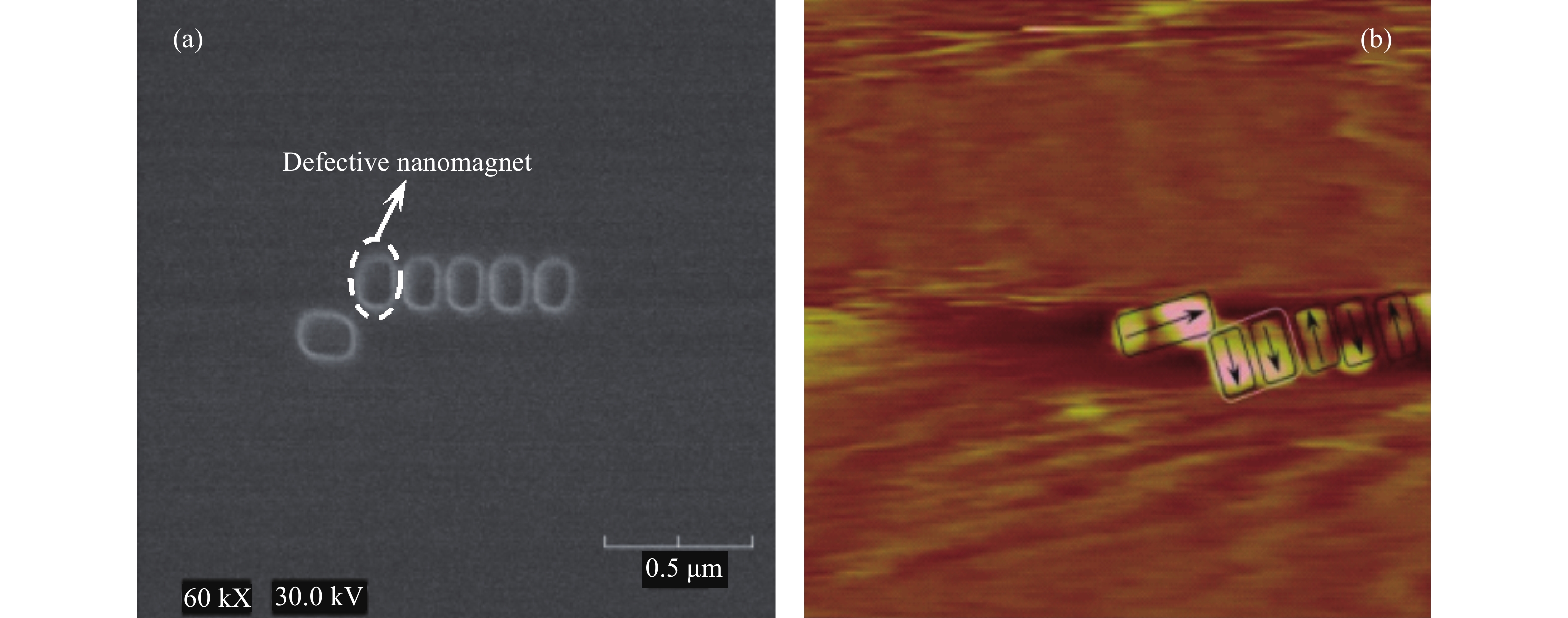
Fig. 5.  (Color online) Experimental results of defective interconnect wire shown in Fig. 3. (a) SEM image of interconnect wire subjected to edge imperfection. (b) The magnetic force microscopy (MFM) image of defective interconnect wire.

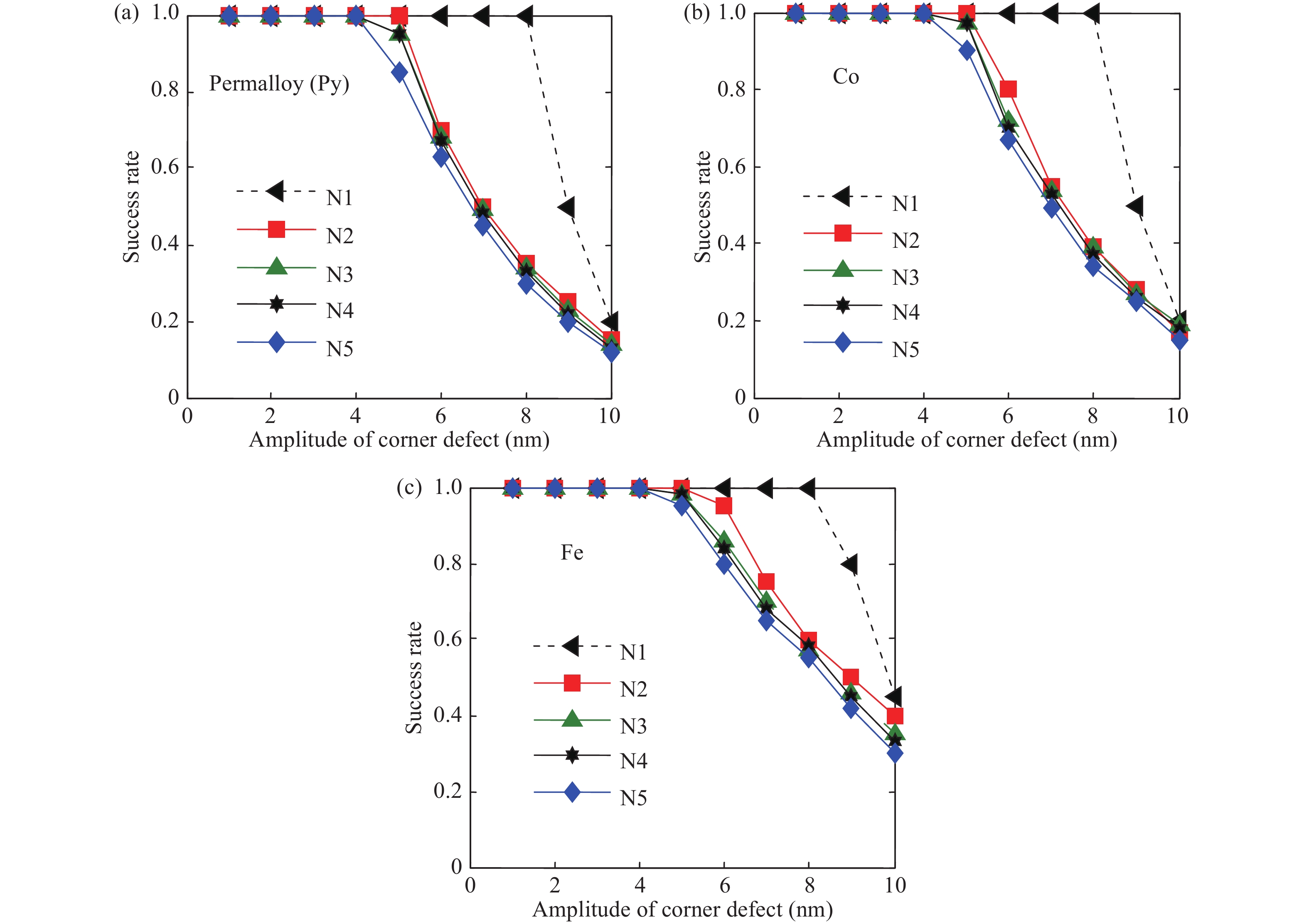
Fig. 6.  (Color online) Number of successes of each nanomagnet element versus the defect amplitude for different materials. (a) Permalloy material. (b) Co material. (c) Fe material.

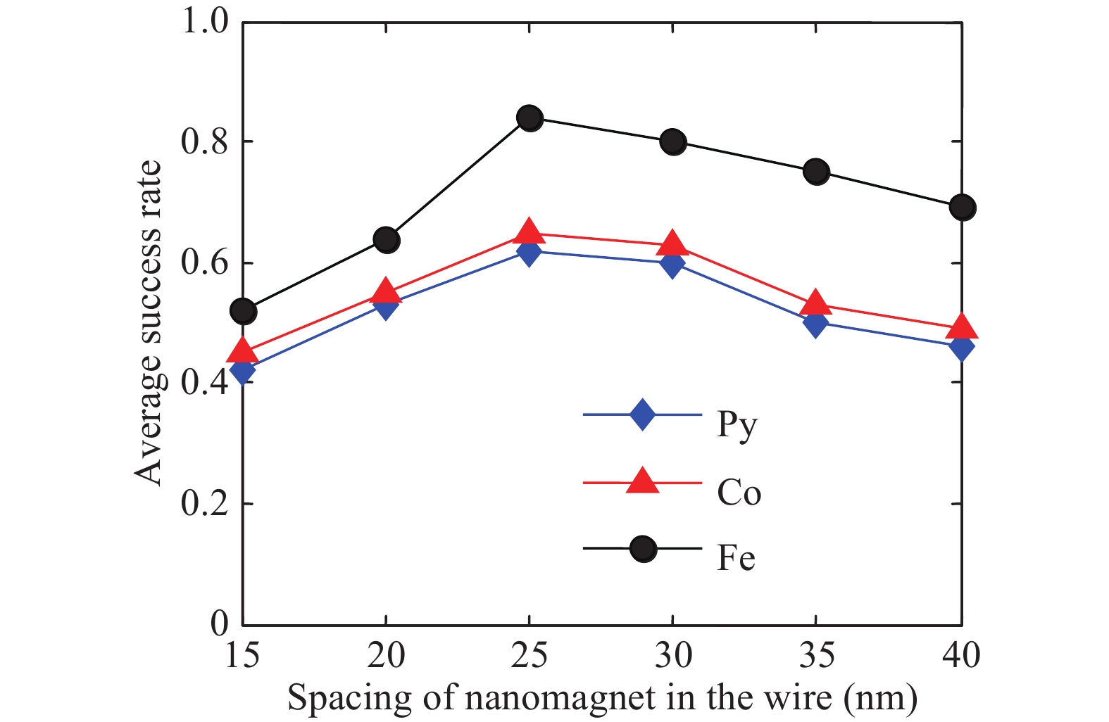
Fig. 7.  (Color online) Nanomagnet spacing effects of defective interconnect wire fabricated with three different materials.

Table 1.   Three materials parameters and device sizes.

Parameter Permalloy Co Fe
MS (A/m) 8 × 10⁵ 10 × 105 17.5 × 10⁵
A (J/m) 10.5 × 10⁻¹² 13 × 10−12 21 × 10−12
Size (nm3) 60 × 100 × 30 60 × 100 × 10 60 × 100 × 6
DownLoad: CSV
[1]
Bernstein K, Cavin III R K, Porod W, et al. Device and architecture outlook for beyond CMOS switches. Proc IEEE, 2010, 98(12): 2169 doi: 10.1109/JPROC.2010.2066530
[2]
Tóth G, Lent C S. Quantum computing with quantum-dot cellular automata. Phys Rev A, 2001, 63(5): 052315 doi: 10.1103/PhysRevA.63.052315
[3]
Colci M, Johnson M. Dipolar coupling between nanopillar spin valves and magnetic quantum cellular automata arrays. IEEE Trans Nanotechnol, 2013, 12(5): 824 doi: 10.1109/TNANO.2013.2275033
[4]
Imre A, Csaba G, Ji L, et al. Majority logic gate for magnetic quantum-dot cellular automata. Science, 2006, 311(5758): 205 doi: 10.1126/science.1120506
[5]
Yang X K, Cai L, Zhang B, et al. Micromagnetic simulation of exploratory magnetic logic device with missing corner defect. J Magn Magn Mater, 2015(11): 391 doi: 10.1016/j.jmmm.2015.06.068
[6]
Allwood D A, Xiong G, Faulkner C C, et al. Magnetic domain-wall logic. Science, 2005, 309(5741): 1688 doi: 10.1126/science.1108813
[7]
Suh D I, Kil J P, Kim K W, et al. A single magnetic tunnel junction representing the basic logic functions-NAND, NOR, and IMP. IEEE Electron Device Letters, 2015, 36(4): 402 doi: 10.1109/LED.2015.2406881
[8]
Fong X, Kim Y, Yogendra K, et al. Spin-transfer torque devices for logic and memory: prospects and perspectives. IEEE Trans Comput-Aid Des Integr Circuits Syst, 2016, 35(1): 1 doi: 10.1109/TCAD.2015.2481793
[9]
Hu L, Hesjedal T. Micromagnetic investigation of the S-state reconfigurable logic element. IEEE Trans Magnet, 2012, 48(7): 2103 doi: 10.1109/TMAG.2012.2183607
[10]
Imtaar M A, Yadav A, Epping A, et al. Nanomagnet fabrication using nanoimprint lithography and electrodeposition. IEEE Trans Nanotechnol, 2013, 12(4): 547 doi: 10.1109/TNANO.2013.2257833
[11]
Yang X K, Cai L, Wang S Z, et al. Reliability and performance evaluation of QCA devices with rotation cell defect. IEEE Trans Nanotechnol, 2012, 11(9): 1009 doi: 10.1109/TNANO.2012.2211613
[12]
Niemier M, Varga E, Bernstein G H, et al. Shape engineering for controlled switching with nanomagnet logic. IEEE Trans Nanotechnol, 2012, 11(2): 220 doi: 10.1109/TNANO.2010.2056697
[13]
Shah F A, Sankar V K, Li P, et al. Compensation of orange-peel coupling effect in magnetic tunnel junction free layer via shape engineering for nanomagnet logic applications. J Appl Phys, 2014, 115(17): 17B902 doi: 10.1063/1.4863935
[14]
Spedalieri F M, Jacob A P, Nikonov D E, et al. Performance of magnetic quantum cellular automata and limitations due to thermal noise. IEEE Trans Nanotechnol, 2011, 10(3): 537 doi: 10.1109/TNANO.2010.2050597
[15]
Alam M T, Kurtz S J, Siddiq M. On-chip clocking of nanomagnet logic lines and gates. IEEE Trans Nanotechnol, 2012, 11(2): 273 doi: 10.1109/TNANO.2011.2169983
[16]
Chunsheng E, Rantschler J, Khizroev S, et al. Micromagnetics of signal propagation in magnetic cellular logic data channels. J Appl Phys, 2008, 104(5): 054311 doi: 10.1063/1.2975836
[17]
Donahue M J, Porter D G. OOMMF user's guide. Version 1.0. Interagency Report NISTIR 6376, National Institute of Standards and Technology (NIST), Gaithersburg, MD
[18]
Yang X K, Cai L, Wang J H, et al. Experimental study of magnetic quantum-dot cellular automata function arrays. Acta Phys Sin, 2012, 61(4): 047502
[19]
Kumari A, Bhanja S. Landauer clocking for magnetic cellular automata (MCA) arrays. IEEE Trans Very Large Scale Integr Syst, 2011, 19(4): 714 doi: 10.1109/TVLSI.2009.2036627
[20]
D’Souza N, Fashami M S, Bandyopadhyay S, et al. Experimental clocking of nanomagnets with strain for ultralow power boolean logic. Nano Lett, 2016, 16(2): 1069 doi: 10.1021/acs.nanolett.5b04205
[21]
Gross L, Schlittler R R, Meyer G, et al. Magnetologic devices fabricated by nanostencil lithography. Nanotechnology, 2010, 21(32): 325301 doi: 10.1088/0957-4484/21/32/325301
  • Search

    Advanced Search >>

    GET CITATION

    shu

    Export: BibTex EndNote

    Article Metrics

    Article views: 3519 Times PDF downloads: 34 Times Cited by: 0 Times

    History

    Received: 22 June 2017 Revised: 24 July 2017 Online: Uncorrected proof: 24 January 2018Accepted Manuscript: 02 February 2018Published: 02 February 2018

    Catalog

      Email This Article

      User name:
      Email:*请输入正确邮箱
      Code:*验证码错误
      Bin Zhang, Xiaokuo Yang, Jiahao Liu, Weiwei Li, Jie Xu. Reliability analysis of magnetic logic interconnect wire subjected to magnet edge imperfections[J]. Journal of Semiconductors, 2018, 39(2): 024004. doi: 10.1088/1674-4926/39/2/024004 ****B Zhang, X K Yang, J H Liu, W W Li, J Xu. Reliability analysis of magnetic logic interconnect wire subjected to magnet edge imperfections[J]. J. Semicond., 2018, 39(2): 024004. doi: 10.1088/1674-4926/39/2/024004.
      Citation:
      Bin Zhang, Xiaokuo Yang, Jiahao Liu, Weiwei Li, Jie Xu. Reliability analysis of magnetic logic interconnect wire subjected to magnet edge imperfections[J]. Journal of Semiconductors, 2018, 39(2): 024004. doi: 10.1088/1674-4926/39/2/024004 ****
      B Zhang, X K Yang, J H Liu, W W Li, J Xu. Reliability analysis of magnetic logic interconnect wire subjected to magnet edge imperfections[J]. J. Semicond., 2018, 39(2): 024004. doi: 10.1088/1674-4926/39/2/024004.

      Reliability analysis of magnetic logic interconnect wire subjected to magnet edge imperfections

      DOI: 10.1088/1674-4926/39/2/024004
      Funds:

      Project supported by the National Natural Science Foundation of China (No. 61302022) and the Scientific Research Foundation for Postdoctor of Air Force Engineering University (Nos. 2015BSKYQD03, 2016KYMZ06).

      More Information

      Catalog

        /

        DownLoad:  Full-Size Img  PowerPoint
        Return
        Return