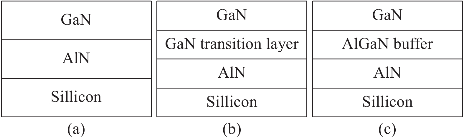
Processing math: 100%
J. Semicond. > 2018, Volume 39 > Issue 3 > 033006

SEMICONDUCTOR MATERIALS

Analysis of the growth of GaN epitaxy on silicon

Danmei Zhao1, and Degang Zhao2

+ Author Affiliations

 Corresponding author: Danmei Zhao, E-mail: 986698015@qq.com

DOI: 10.1088/1674-4926/39/3/033006

PDF

Turn off MathJax

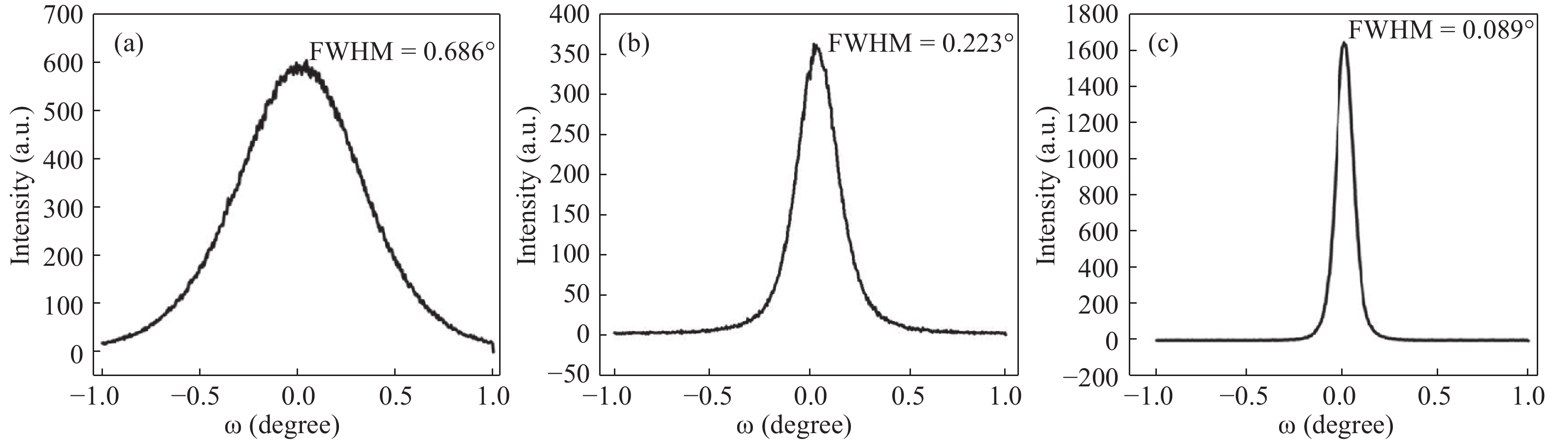
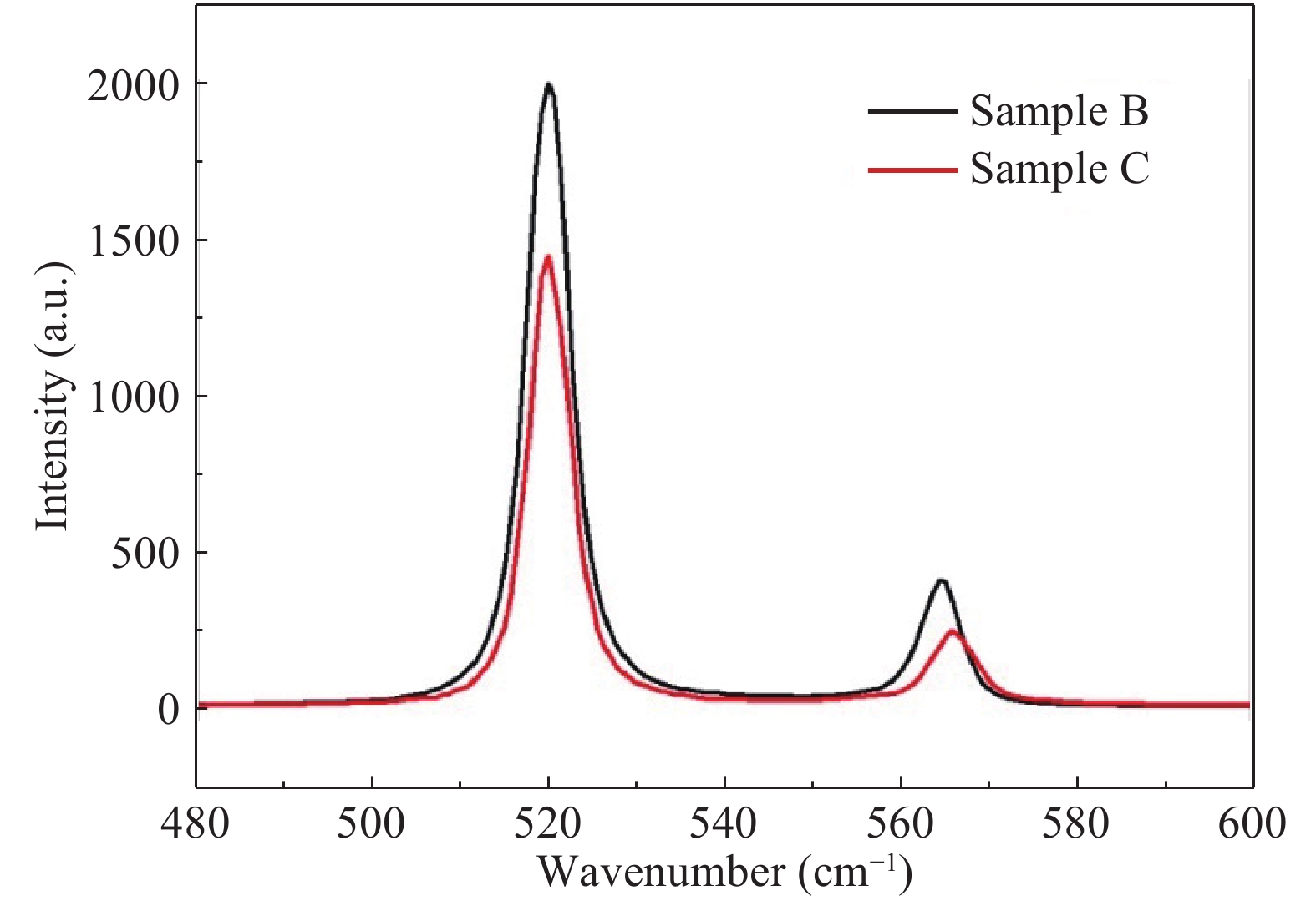
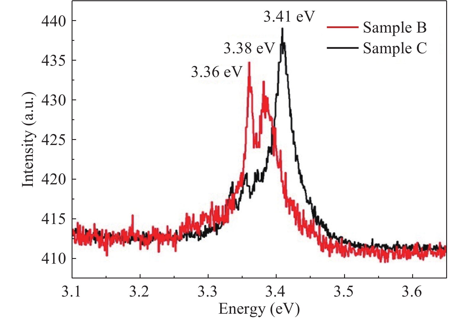
Abstract: Due to the great potential of GaN based devices, the analysis of the growth of crack-free GaN with high quality has always been a research hotspot. In this paper, two methods for improving the property of the GaN epitaxial layer on Si (111) substrate are researched. Sample A, as a reference, only has an AlN buffer between the Si substrate and the epitaxy. In the following two samples, a GaN transition layer (sample B) and an AlGaN buffer (sample C) are grown on the AlN buffer separately. Both methods improve the quality of GaN. Meanwhile, using the second method, the residual tensile thermal stress decreases. To further study the impact of the two introduced layers, we investigate the stress condition of GaN epitaxial layer by Raman spectrum. According to the Raman spectrum, the calculated residual stress in the GaN epitaxial layer is approximately 0.72 GPa for sample B and 0.42 GPa for sample C. The photoluminescence property of GaN epitaxy is also investigated by room temperature PL spectrum.

Key words: GaNstressMOCVD

The growth of GaN epitaxy on Si has become very popular for its potential for uses in light emitting diodes, high-frequency electronic devices, ultraviolet detectors, and related technologies[1, 2]. Although some GaN based devices are already commercialized, it is still a challenge to produce high quality material, due to the lack of GaN homo-epitaxial substrates. The GaN epitaxial layer is usually grown on hetero-epitaxial substrates (Sapphire, SiC, Si). Sapphire is one of the favorable substrates for it is available in a large diameter dimension; however, its low thermal and electrical conductivity limits its application, and it shows a high hardness hampering wafer dicing. Compared to SiC, silicon substrate is a more cost effective choice for GaN growth[35]. As the most favored substrate orientation for wurtzite nitrides, Si (111) substrate has a lattice mismatch of 17% with GaN and 19% with AlN. It is easy for GaN epitaxy to generate high dislocation densities. Meanwhile, the large thermal mismatch of 56% also leads to large tensile strain during cooling down time[6]. Many methods have been used to reduce the tensile and improve the crystalline quality of GaN[710].

This experiment introduced two methods to improve the quality and strain condition of GaN. By comparing the XRD, Raman spectrum and PL spectrum, this article illustrates the two different growth mechanisms of the two methods.

The experiment is completed by metal-organic chemical vapor deposition (MOCVD). TMGa, TMAl, and NH3 are used as Ga, Al, and N precursors, respectively. H2 is the carrier gases. The structures of samples with different growth methods are shown in Fig. 1. In sample A, as a reference, only AlN buffer is adopted, followed by GaN epitaxial layer. In sample B, the GaN transition layer follows the AlN buffer. In sample C, the AlGaN buffer is introduced. The AlN buffers are 100 nm for all the samples. For sample B, GaN transition layer is grown with the V/III ratio of 590 for 100 s, while all the GaN epitaxial layers are grown with the V/III ratio of 2000. For sample C, the AlGaN buffer is 300 nm.

Figure  1.  The schematic diagrams of structures for (a) sample A, (b) sample B, and (c) sample C.

In this study, the crystal quality of GaN epitaxial layer is investigated with X-ray diffraction (XRD). It is also very important to understand the knowledge of the stress condition or strain for improving the properties of nitride-based devices. The Raman spectra have been recorded at room temperature and the He–Ne laser (632.8 nm) is used for the excitation. The photoluminescence spectrum (PL) is used to analyse the optical properties.

The full widths at X-ray diffraction half maximum (FWHMs) of GaN on the (0002) plane of samples A, B and C are 0.686°, 0.223° and 0.089° respectively, as shown in Fig. 2. It shows that a GaN epitaxial layer grown directly on the AlN buffer turns out to have a poor quality. With the introduced GaN transition layer or the AlGaN buffer, the crystalline quality of GaN epitaxy is greatly improved, and the latter method is better.

Figure  2.  The FWHMs of (0002) XRD of different samples: (a) sample A, (b) sample B, and (c) sample C.

Raman spectra of samples B and C were measured at room temperature to analyse the stress condition of the samples. As shown in Fig. 3, there are two peaks in both samples in the range from 480 to 600 cm−1. The peak located at 520 cm−1 is the optical phonon peak of Si. The nominal E2phonon peaks of samples B and C are located at 564 and 565.8 cm−1 respectively. The nominal E2 phonon peak frequency of the relaxed GaN bulk material[11] is 567.6 cm−1. As it is reported, the move of the E2 peak frequency is attributed to different stress conditions (red shift corresponds to tensile stress and blue shift corresponds to compressive stress)[12]. Obviously, both samples are under tensile stress. In the linear approximation, the biaxial stress σxx can be calculated by the following equation with the deviation in E2 peak frequency if the linear stress coefficient Kγ is known:

Figure  3.  (Color online) Raman spectra of GaN films with different structures: sample B and sample C.
Δωγ=Kγσxx. (1)

According to the stress coefficient of 4.3 cm−1GPa−1 for GaN[13], the calculated residual stress in the GaN epitaxial layer is approximately 0.72 GPa for sample B and 0.42 GPa for sample C. It is obvious that, compared with sample B, which introduces the GaN transition layer, sample C with AlGaN buffer expresses much less residual tensile stress.

This result is probably attributed to the different growth mechanism of the two samples. For sample B, by introducing the GaN transition layer, GaN islands with proper density and size can be formed on the AlN buffer layer. By controlling the growth and merge of the islands, comparative improvement of the crystal quality of the GaN epitaxial layer is achieved (Details are shown in Ref. [14]). For sample C, more compressive stress is built up in the subsequent GaN due to the introduction of AlGaN buffer[15]. The compressive stress leads to larger dislocation inclination and consequently to reduction of the density in a-type dislocations[16]. What is more, the higher compressive stress leads to less residual tensile stress to GaN epitaxy.

The scanning curves of room temperature PL of samples B and C are shown in Fig. 4. The peaks of the band gap edge of hexagonal GaN for samples B and C are located at 3.38 and 3.41 eV separately. The difference of the peak location is mainly attributed to the different residual stress of GaN epitaxial layers[17]. Besides, there is an additional peak located at 3.36 eV for sample B. The mechanism of this peak is not fully explained. It may be attributed to the low crystalline quality or stacking faults (SFs)[17]. There are also some additional peaks located lower than the band gap energy for sample C, which may also be attributed to stacking faults (SFs). As shown in Fig. 4, the PL intensity of sample C is higher than sample B. Furthermore, the PL intensity of the band gap edge is much higher than that of peaks located lower for sample C. For sample B, the PL intensity of the band gap edge is lower than that of peaks located at 3.36 eV. It indicates that the crystal quality of sample C is higher than sample B, which is consistent with the XRD result.

Figure  4.  (Color online) Scanned spectra of GaN films with different structure by room temperature PL: sample B and sample C.

In this study, two additional methods for improving the property of GaN films on Si (111) substrates are researched. The methods are proposed to improve the crystalline quality and reduce the residual tensile stress of the GaN epitaxial layer. The first method is to introduce a GaN transition layer. For the second method, AlGaN buffer is grown on AlN buffer. Both methods result in a significant improvement of the quality of GaN epitaxial layer. What is more, with the second method, the residual tensile thermal stress decreases. This is because both methods lead to a larger dislocation inclination and consequently to a reduction of the a-type dislocation density. Besides, more compressive stress is built up in the subsequent GaN due to the introduction of AlGaN buffer and the higher compressive stress leads to less residual tensile stress to GaN epitaxy.


[1]
Lenka H, Meersschaut J, Kandaswamy P K, et al. Dislocation density and tetragonal distortion of a GaN epilayer on Si (111): A comparative RBS/C and TEM study. Nucl Instrum Meth Phys Res B, 2014, 331: 69 doi: 10.1016/j.nimb.2014.02.014
[2]
Cong G W , Lu Y, Peng W Q, et al. Design of the low-temperature AlN interlayer for GaN grown on Si (111) substrate. J Cryst Growth, 2005, 276(3/4): 381 doi: 10.1016/j.jcrysgro
[3]
Mauder C, Booker I D, Fahle D, et al. On the anisotropic wafer curvature of GaN-based eterostructures on Si(110) substrates grown by MOVPE. J Cryst Growth, 2011, 315(1): 220 doi: 10.1016/j.jcrysgro.2010.08.049
[4]
Yoshida S, Li J, Ikeda N. AlGaN/GaN field effect Schottky barrier diode (FESBD). Phys Stat Sol C, 2005, 2(7): 2602 doi: 10.1002/(ISSN)1610-1642
[5]
Wang M Y, Zhang G A, Zhang Z J, et al. Study on GaN-based light emitting diodes grownon 4-in. Si(111) substrate. Opt Commun, 2014, 326: 20 doi: 10.1016/j.optcom.2014.04.002
[6]
Luo R H, Xiang P, Liu M G, et al. High quality GaN grown on Si(111) using fast coalescence growth. Jpn J Appl Phys, 2011, 50: 121001
[7]
Tungare M, Weng X J, Leathersich J M, et al. Modification of dislocation behavior in GaN overgrown on engineered AlN film-on-bulk Si substrate. J Appl Phys, 2013, 113(16): 3518 doi: 10.1063/1.4798598
[8]
Kim M H, Do Y G, Kang H C, et al. Effects of step-graded AlxGa1–xN interlayer on properties of GaN grown on Si(111) using ultrahigh vacuum chemical vapor deposition. Appl Phys Lett, 2001, 79(17): 2713 doi: 10.1063/1.1412824
[9]
Benjamin L, Han J, Sun Q. Strain relaxation and dislocation reduction in AlGaN step-graded buffer for crack-free GaN on Si (111). Phys Status Solidi C, 2004, 11(3/4): 437 doi: 10.1002/pssc.201300690
[10]
Ni Y Q, He Z Y, Zhong J, et al. Electrical properties of MOCVD-grown GaN on Si (111) substrates with low-temperature AlN interlayers. Chin Phys B, 2013, 22(8): 088104
[11]
Tung L T, Lin K L, Chang E Y, et al. Photoluminescence and Raman studies of GaN films grown by MOCVD. J Phys: Conf Ser, 2009, 187: 012021 doi: 10.1088/1742-6596/187/1/012021
[12]
Martínez O, Avella M, Jiménez J, et al. Optical properties of epitaxial lateral overgrowth GaN structures studied by Raman and cathode luminescence spectroscopies. J Appl Phys, 2004, 96: 3639 doi: 10.1063/1.1786670
[13]
Zhao D G, Xu S J, Xie M H, et al. Stress and its effect on optical properties of GaN epilayers grown on Si(111), 6H-SiC(0001), and c-plane sapphire. Appl Phys Lett, 2003, 83(4): 677 doi: 10.1063/1.1592306
[14]
Zhao D M, Zhao D G, Jiang D S, et al. Impact of GaN transition layers in the growth of GaN epitaxial layer on silicon. J Semicond, 2015, 36(6): 063003 doi: 10.1088/1674-4926/36/6/063003
[15]
Fritze S, Drechsel P, Stauss P, et al. A role of low-temperature AlGaN interlayers in thick GaN on silicon by metalorganic vapor phase epitaxy. J Appl Phys, 2012, 111: 124505
[16]
Able A, Wegscheider W, Engl K, et al. Growth of crack-free GaN on Si(111) with graded AlGaN buffer layers. J Cryst Growth, 2005, 276: 415
[17]
Zhao D M, Zhao D G, Jiang D S, et al. Temperature-dependent photoluminescence spectra of GaN epitaxial layer grown on Si (111) substrate. Chin Phys B, 2015, 24(10): 108101 doi: 10.1088/1674-1056/24/10/108101
Fig. 1.  The schematic diagrams of structures for (a) sample A, (b) sample B, and (c) sample C.

Fig. 2.  The FWHMs of (0002) XRD of different samples: (a) sample A, (b) sample B, and (c) sample C.

Fig. 3.  (Color online) Raman spectra of GaN films with different structures: sample B and sample C.

Fig. 4.  (Color online) Scanned spectra of GaN films with different structure by room temperature PL: sample B and sample C.

[1]
Lenka H, Meersschaut J, Kandaswamy P K, et al. Dislocation density and tetragonal distortion of a GaN epilayer on Si (111): A comparative RBS/C and TEM study. Nucl Instrum Meth Phys Res B, 2014, 331: 69 doi: 10.1016/j.nimb.2014.02.014
[2]
Cong G W , Lu Y, Peng W Q, et al. Design of the low-temperature AlN interlayer for GaN grown on Si (111) substrate. J Cryst Growth, 2005, 276(3/4): 381 doi: 10.1016/j.jcrysgro
[3]
Mauder C, Booker I D, Fahle D, et al. On the anisotropic wafer curvature of GaN-based eterostructures on Si(110) substrates grown by MOVPE. J Cryst Growth, 2011, 315(1): 220 doi: 10.1016/j.jcrysgro.2010.08.049
[4]
Yoshida S, Li J, Ikeda N. AlGaN/GaN field effect Schottky barrier diode (FESBD). Phys Stat Sol C, 2005, 2(7): 2602 doi: 10.1002/(ISSN)1610-1642
[5]
Wang M Y, Zhang G A, Zhang Z J, et al. Study on GaN-based light emitting diodes grownon 4-in. Si(111) substrate. Opt Commun, 2014, 326: 20 doi: 10.1016/j.optcom.2014.04.002
[6]
Luo R H, Xiang P, Liu M G, et al. High quality GaN grown on Si(111) using fast coalescence growth. Jpn J Appl Phys, 2011, 50: 121001
[7]
Tungare M, Weng X J, Leathersich J M, et al. Modification of dislocation behavior in GaN overgrown on engineered AlN film-on-bulk Si substrate. J Appl Phys, 2013, 113(16): 3518 doi: 10.1063/1.4798598
[8]
Kim M H, Do Y G, Kang H C, et al. Effects of step-graded AlxGa1–xN interlayer on properties of GaN grown on Si(111) using ultrahigh vacuum chemical vapor deposition. Appl Phys Lett, 2001, 79(17): 2713 doi: 10.1063/1.1412824
[9]
Benjamin L, Han J, Sun Q. Strain relaxation and dislocation reduction in AlGaN step-graded buffer for crack-free GaN on Si (111). Phys Status Solidi C, 2004, 11(3/4): 437 doi: 10.1002/pssc.201300690
[10]
Ni Y Q, He Z Y, Zhong J, et al. Electrical properties of MOCVD-grown GaN on Si (111) substrates with low-temperature AlN interlayers. Chin Phys B, 2013, 22(8): 088104
[11]
Tung L T, Lin K L, Chang E Y, et al. Photoluminescence and Raman studies of GaN films grown by MOCVD. J Phys: Conf Ser, 2009, 187: 012021 doi: 10.1088/1742-6596/187/1/012021
[12]
Martínez O, Avella M, Jiménez J, et al. Optical properties of epitaxial lateral overgrowth GaN structures studied by Raman and cathode luminescence spectroscopies. J Appl Phys, 2004, 96: 3639 doi: 10.1063/1.1786670
[13]
Zhao D G, Xu S J, Xie M H, et al. Stress and its effect on optical properties of GaN epilayers grown on Si(111), 6H-SiC(0001), and c-plane sapphire. Appl Phys Lett, 2003, 83(4): 677 doi: 10.1063/1.1592306
[14]
Zhao D M, Zhao D G, Jiang D S, et al. Impact of GaN transition layers in the growth of GaN epitaxial layer on silicon. J Semicond, 2015, 36(6): 063003 doi: 10.1088/1674-4926/36/6/063003
[15]
Fritze S, Drechsel P, Stauss P, et al. A role of low-temperature AlGaN interlayers in thick GaN on silicon by metalorganic vapor phase epitaxy. J Appl Phys, 2012, 111: 124505
[16]
Able A, Wegscheider W, Engl K, et al. Growth of crack-free GaN on Si(111) with graded AlGaN buffer layers. J Cryst Growth, 2005, 276: 415
[17]
Zhao D M, Zhao D G, Jiang D S, et al. Temperature-dependent photoluminescence spectra of GaN epitaxial layer grown on Si (111) substrate. Chin Phys B, 2015, 24(10): 108101 doi: 10.1088/1674-1056/24/10/108101
1

Unstrained InAlN/GaN heterostructures grown on sapphire substrates by MOCVD

Bo Liu, Jiayun Yin, Yuanjie Lü, Shaobo Dun, Xiongwen Zhang, et al.

Journal of Semiconductors, 2014, 35(11): 113005. doi: 10.1088/1674-4926/35/11/113005

2

Microstructural properties of over-doped GaN-based diluted magnetic semiconductors grown by MOCVD

Tao Zhikuo, Zhang Rong, Xiu Xiangqian, Cui Xugao, Li Li, et al.

Journal of Semiconductors, 2012, 33(7): 073002. doi: 10.1088/1674-4926/33/7/073002

3

High quality GaN-based LED epitaxial layers grown in a homemade MOCVD system

Yin Haibo, Wang Xiaoliang, Ran Junxue, Hu Guoxin, Zhang Lu, et al.

Journal of Semiconductors, 2011, 32(3): 033002. doi: 10.1088/1674-4926/32/3/033002

4

Surface morphology of [11-20] a-plane GaN growth by MOCVD on [1-102] r-plane sapphire

Xu Shengrui, Hao Yue, Duan Huantao, Zhang Jincheng, Zhang Jinfeng, et al.

Journal of Semiconductors, 2009, 30(4): 043003. doi: 10.1088/1674-4926/30/4/043003

5

Effect of a Metal Buffer Layer on GaN Grown on Si(111) by Gas Source Molecular Beam Epitaxy with Ammonia

Lin Guoqiang, Zeng Yiping, Wang Xiaoliang, Liu Hongxin

Journal of Semiconductors, 2008, 29(10): 1998-2002.

6

Studies on the Butt-Joint of a InGaAsP-Waveguide Realized with Metalorganic Vapor Phase Epitaxy

Zhang Ruikang, Dong Lei, Yu Yonglin, Wang Dingli, Zhang Jing, et al.

Journal of Semiconductors, 2008, 29(6): 1177-1179.

7

Defect Cluster-Induced X-Ray Diffuse Scattering in GaN Films Grown by MOCVD

Ma Zhifang, Wang Yutian, Jiang Desheng, Zhao Degang, Zhang Shuming, et al.

Journal of Semiconductors, 2008, 29(7): 1242-1245.

8

Optimization and Analysis of Magnesium Doping in MOCVD Grown p-GaN

Zhang Xiaomin, Wang Yanjie, Yang Ziwen, Liao Hui, Chen Weihua, et al.

Journal of Semiconductors, 2008, 29(8): 1475-1478.

9

AIGaN-Based Multi-Type Distributed Bragg Reflectors Grown by MOCVD

Liu Bin, Zhang Rong, Xie Zili, Ji Xiaoli, Li Liang, et al.

Chinese Journal of Semiconductors , 2007, 28(S1): 492-495.

10

Epitaxial Lateral Overgrowth of Gallium Nitride on Sapphire

Zhang Wei, Hao Qiuyan, Jing Weina, Liu Caichi, Feng Yuchun, et al.

Chinese Journal of Semiconductors , 2007, 28(S1): 33-36.

11

Growth and Stress Analysis of a-Plane GaN Films Grown on r-Plane Sapphire Substrate with a Two-Step AlN Buffer Layer

Yan Jianfeng, Zhang Jie, Guo Liwei, Zhu Xueliang, Peng Mingzeng, et al.

Chinese Journal of Semiconductors , 2007, 28(10): 1562-1567.

12

Epitaxial Growth of Atomically Flat AlN Layers on Sapphire Substrate by Metal Organic Chemical Vapor Deposition

Zhao Hong, Zou Zeya, Zhao Wenbai, Liu Ting, Yang Xiaobo, et al.

Chinese Journal of Semiconductors , 2007, 28(10): 1568-1573.

13

Growth of High AI Content AIGaN Epilayer by MOCVD

Wang Xiaoyan, Wang Xiaoliang, Hu Guoxin, Wang Baozhu, Li Jianping, et al.

Chinese Journal of Semiconductors , 2007, 28(S1): 193-196.

14

Growth of GaN on Si(1 l 1) by Inserting 5AI/AIN Buffer Layer

Guo Lunchun, Wang Xiaoliang, Hu Guoxin, Li Jianping, Luo Weijun, et al.

Chinese Journal of Semiconductors , 2007, 28(S1): 234-237.

15

Growth and Characterization of m Plane GaN Material by MOCVD

Xie Zili, Zhang Rong, Han Ping, Liu Chengxiang, Xiu XiangQian, et al.

Chinese Journal of Semiconductors , 2007, 28(S1): 249-252.

16

Numerical Simulation of Gas Phase and Surface Reaction for Growth of GaN by MOCVD

Gao Lihua, Yang Yunke, Chen Haixin, Fu Song

Chinese Journal of Semiconductors , 2007, 28(S1): 245-248.

17

MOCVD-Grown AlGaN/AlN/GaN HEMT Structure with High Mobility GaN Thin Layer as Channel on SiC

Wang Xiaoliang, Hu Guoxin, Ma Zhiyong, Xiao Hongling, Wang Cuimei, et al.

Chinese Journal of Semiconductors , 2006, 27(9): 1521-1525.

18

ZnO Thin Film Growth by Metal Organic Chemical Vapor Deposition and Its Back Contact Application in Solar Cells

Chen Xinliang, Xu Buheng, Xue Junming, Zhao Ying, Zhang Xiaodan, et al.

Chinese Journal of Semiconductors , 2005, 26(12): 2363-2368.

19

Epitaxial Lateral Overgrowth of High Quality GaN by MOCVD

Chen Jun, Zhang Jicai, Zhang Shuming, Zhu Jianjun, Yang Hui, et al.

Chinese Journal of Semiconductors , 2005, 26(S1): 106-108.

20

High Resistivity GaN Film Grown by MOCVD

Fang Cebao, Wang Xiaoliang, Liu Chao, Hu Guoxin, Wang Junxi, et al.

Chinese Journal of Semiconductors , 2005, 26(S1): 91-93.

1. Li, Q., Liu, G., Wang, S. et al. The effect of GaN single crystal substrate characteristics on homo-epitaxial GaN films. Surfaces and Interfaces, 2025. doi:10.1016/j.surfin.2024.105554
2. Langpoklakpam, C., Liu, A.-C., Hsiao, Y.-K. et al. Vertical GaN MOSFET Power Devices. Micromachines, 2023, 14(10): 1937. doi:10.3390/mi14101937
3. Zhou, Y., Zhou, S., Wan, S. et al. Tuning the interlayer microstructure and residual stress of buffer-free direct bonding GaN/Si heterostructures. Applied Physics Letters, 2023, 122(8): 082103. doi:10.1063/5.0135138
4. Zhou, S., Wan, S., Zou, B. et al. Interlayer Investigations of GaN Heterostructures Integrated into Silicon Substrates by Surface Activated Bonding. Crystals, 2023, 13(2): 217. doi:10.3390/cryst13020217
5. Zhang, Z.-Z., Yang, J., Zhao, D.-G. et al. Influence of the lattice parameter of the AlN buffer layer on the stress state of GaN film grown on (111) Si. Chinese Physics B, 2023, 32(2): 028101. doi:10.1088/1674-1056/ac6b2b
6. Jeong, H.. Spectroscopic analysis and two-dimensional confocal photoluminescence properties of GaN films grown on silicon and sapphire substrates. Journal of the Korean Physical Society, 2022, 81(8): 784-789. doi:10.1007/s40042-022-00624-6
7. Nguyen, V.-T., Fang, T.-H. Material removal mechanism and deformation characteristics of GaN surface at the nanoscale. Micro and Nanostructures, 2022. doi:10.1016/j.spmi.2022.107159
8. Nguyen, V.-T., Fang, T.-H. Material removal mechanism and deformation characteristics of GaN surface at the nanoscale. Superlattices and Microstructures, 2022. doi:10.1016/j.spmi.2022.107159
9. Meneghini, M., De Santi, C., Abid, I. et al. GaN-based power devices: Physics, reliability, and perspectives. Journal of Applied Physics, 2021, 130(18): 181101. doi:10.1063/5.0061354
10. Jia, T., Dong, H., Jia, Z. et al. Influence of indium composition of n waveguide layer on photoelectric performance of GaN-based green laser diode | [n波导层铟组分对GaN基绿光激光二极管光电性能的影响]. Hongwai Yu Jiguang Gongcheng Infrared and Laser Engineering, 2021, 50(10): 20200489. doi:10.3788/IRLA20200489
11. Zhang, Y., Liang, F., Zhao, D. et al. Monotonic variation in carbon-related defects with Fermi level in different conductive types of GaN. Aip Advances, 2021, 11(8): 0054483. doi:10.1063/5.0054483
12. Huang, C.-R., Liu, C.-H., Wang, H.-C. et al. The characteristics of 6-inch gan on si rf hemt with high isolation composited buffer layer design. Electronics Switzerland, 2021, 10(1): 1-7. doi:10.3390/electronics10010046
13. Zhang, J., Liu, D., Pan, Y. Suppression of oxygen and carbon impurity deposition in the thermal system of Czochralski monocrystalline silicon. Journal of Semiconductors, 2020, 41(10): 102702. doi:10.1088/1674-4926/41/10/102702
14. Cao, Z.-K., Liu, Z.-S., Jiang, D.-S. et al. Fabrication of High Gain GaN Based PIN Avalanche Diode and Estimation of p-GaN Layer Carrier Concentration | [高增益GaN基PIN雪崩二极管的制备及p-GaN层载流子浓度的估算]. Faguang Xuebao Chinese Journal of Luminescence, 2020, 41(6): 707-713. doi:10.3788/fgxb20204106.0707
15. Zhang, Y., Cheng, Q., Zhang, Y. et al. Catalytic activity and stability of Cu modified ZSM-5 zeolite membrane catalysts prepared by metal-organic chemical vapor deposition for trichloroethylene oxidation. Journal of the Taiwan Institute of Chemical Engineers, 2020. doi:10.1016/j.jtice.2020.01.006
16. Haung, C.R., Liu, C.-H., Wang, H.-C. et al. The characteristics of 6-inch GaN on Si RF HEMT with high isolation composited buffer layer design. 2020.
17. Zhang, Y., Liang, F., Zhao, D. et al. Hydrogen Can Passivate Carbon Impurities in Mg-Doped GaN. Nanoscale Research Letters, 2020, 15(1): 38. doi:10.1186/s11671-020-3263-9
18. Yang, J., Zhao, D.G., Zhu, J.J. et al. Effect of Mg doping concentration of electron blocking layer on the performance of GaN-based laser diodes. Applied Physics B Lasers and Optics, 2019, 125(12): 235. doi:10.1007/s00340-019-7343-4
19. Zhang, H., Huang, Y., Shi, W.-Z. et al. First-principles study on the diffusion dynamics of Al atoms on Si surface | [Al原子在Si表面扩散动力学的第一性原理研究]. Wuli Xuebao Acta Physica Sinica, 2019, 68(20): 207302. doi:10.7498/aps.68.20190783
20. Liang, F., Zhao, D., Jiang, D. et al. Suppression of optical field leakage in GaN-based green laser diode using graded-indium n-InxGa1-xN lower waveguide. Superlattices and Microstructures, 2019. doi:10.1016/j.spmi.2019.106153
21. Wang, J., Feng, M., Zhou, R. et al. GaN-Based ultraviolet microdisk laser diode grown on Si. Photonics Research, 2019, 7(6): B32-B35. doi:10.1364/PRJ.7.000B32
22. Xing, Y., Zhao, D., Jiang, D. et al. Carrier Redistribution Between Two Kinds of Localized States in the InGaN/GaN Quantum Wells Studied by Photoluminescence. Nanoscale Research Letters, 2019. doi:10.1186/s11671-019-2919-9
23. Wang, Q., Yuan, G.-D., Liu, W.-Q. et al. Monolithic semi-polar (1101) InGaN/GaN near white light-emitting diodes on micro-striped Si (100) substrate. Chinese Physics B, 2019, 28(8): 087802. doi:10.1088/1674-1056/28/8/087802
24. Wang, Q., Yuan, G., Wei, T. et al. Multicolored-light emission from InGaN/GaN multiple quantum wells grown by selective-area epitaxy on patterned Si(100) substrates. Journal of Materials Science, 2018, 53(24): 16439-16446. doi:10.1007/s10853-018-2804-4
25. Tan, X., Ji, X., Wei, T. et al. Investigation of pattern-orientation on stress in GaN grown on Si(111) substrate in lateral confinement epitaxy. Superlattices and Microstructures, 2018. doi:10.1016/j.spmi.2018.07.023
  • Search

    Advanced Search >>

    GET CITATION

    Danmei Zhao, Degang Zhao. Analysis of the growth of GaN epitaxy on silicon[J]. Journal of Semiconductors, 2018, 39(3): 033006. doi: 10.1088/1674-4926/39/3/033006
    D M Zhao, D G Zhao. Analysis of the growth of GaN epitaxy on silicon[J]. J. Semicond., 2018, 39(3): 033006. doi: 10.1088/1674-4926/39/3/033006.
    shu

    Export: BibTex EndNote

    Article Metrics

    Article views: 5476 Times PDF downloads: 143 Times Cited by: 25 Times

    History

    Received: 03 June 2017 Revised: 21 August 2017 Online: Uncorrected proof: 24 January 2018Published: 01 March 2018

    Catalog

      Email This Article

      User name:
      Email:*请输入正确邮箱
      Code:*验证码错误
      Danmei Zhao, Degang Zhao. Analysis of the growth of GaN epitaxy on silicon[J]. Journal of Semiconductors, 2018, 39(3): 033006. doi: 10.1088/1674-4926/39/3/033006 ****D M Zhao, D G Zhao. Analysis of the growth of GaN epitaxy on silicon[J]. J. Semicond., 2018, 39(3): 033006. doi: 10.1088/1674-4926/39/3/033006.
      Citation:
      Danmei Zhao, Degang Zhao. Analysis of the growth of GaN epitaxy on silicon[J]. Journal of Semiconductors, 2018, 39(3): 033006. doi: 10.1088/1674-4926/39/3/033006 ****
      D M Zhao, D G Zhao. Analysis of the growth of GaN epitaxy on silicon[J]. J. Semicond., 2018, 39(3): 033006. doi: 10.1088/1674-4926/39/3/033006.

      Analysis of the growth of GaN epitaxy on silicon

      DOI: 10.1088/1674-4926/39/3/033006
      More Information
      • Corresponding author: E-mail: 986698015@qq.com
      • Received Date: 2017-06-03
      • Revised Date: 2017-08-21
      • Available Online: 2018-03-01
      • Published Date: 2018-03-01

      Catalog

        /

        DownLoad:  Full-Size Img  PowerPoint
        Return
        Return