| Citation: |
Zengcheng Li, Bo Feng, Biao Deng, Legong Liu, Yingnan Huang, Meixin Feng, Yu Zhou, Hanmin Zhao, Qian Sun, Huaibing Wang, Xiaoli Yang, Hui Yang. Light output improvement of GaN-based light-emitting diodes grown on Si (111) by a via-thin-film structure[J]. Journal of Semiconductors, 2018, 39(4): 044002. doi: 10.1088/1674-4926/39/4/044002
****
Z C Li, B Feng, B Deng, L G Liu, Y N Huang, M X Feng, Y Zhou, H M Zhao, Q Sun, H B Wang, X L Yang, H Yang. Light output improvement of GaN-based light-emitting diodes grown on Si (111) by a via-thin-film structure[J]. J. Semicond., 2018, 39(4): 044002. doi: 10.1088/1674-4926/39/4/044002.
|
Light output improvement of GaN-based light-emitting diodes grown on Si (111) by a via-thin-film structure
DOI: 10.1088/1674-4926/39/4/044002
More Information
-
Abstract
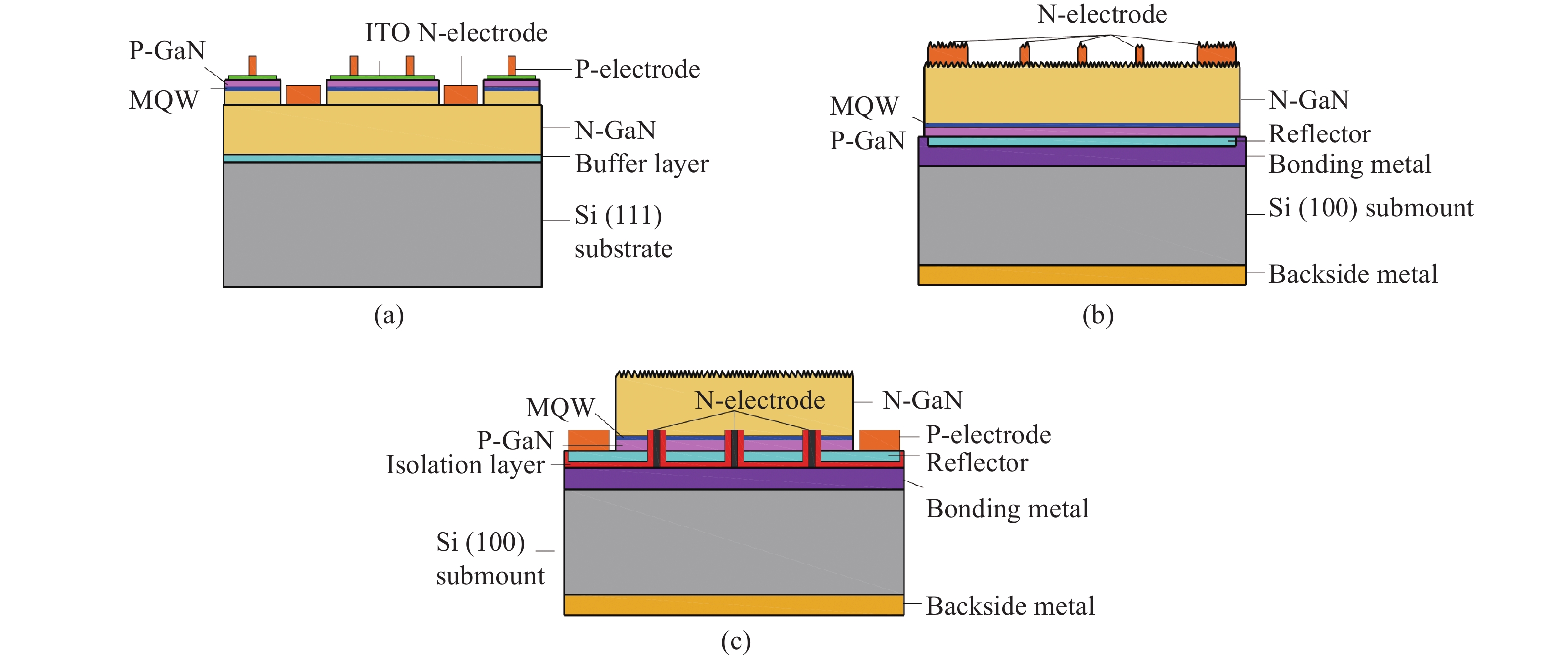
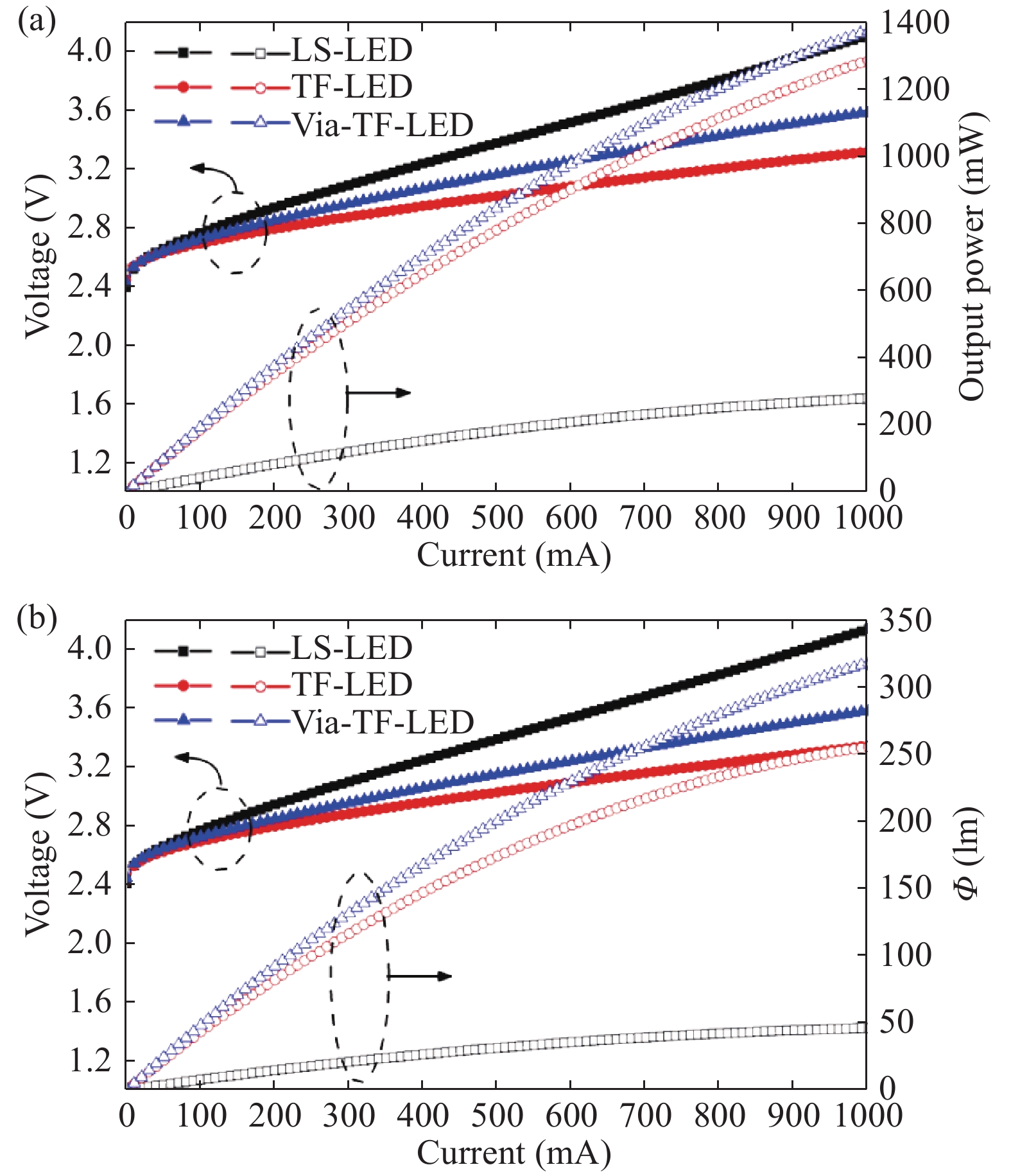
This work reports the fabrication of via-thin-film light-emitting diode (via-TF-LED) to improve the light output power (LOP) of blue/white GaN-based LEDs grown on Si (111) substrates. The as-fabricated via-TF-LEDs were featured with a roughened n-GaN surface and the p-GaN surface bonded to a wafer carrier with a silver-based reflective electrode, together with an array of embedded n-type via pillar metal contact from the p-GaN surface etched through the multiple-quantum-wells (MQWs) into the n-GaN layer. When operated at 350 mA, the via-TF-LED gave an enhanced blue LOP by 7.8% and over 3.5 times as compared to the vertical thin-film LED (TF-LED) and the conventional lateral structure LED (LS-LED). After covering with yellow phosphor that converts some blue photons into yellow light, the via-TF-LED emitted an enhanced white luminous flux by 13.5% and over 5 times, as compared with the white TF-LED and the white LS-LED, respectively. The significant LOP improvement of the via-TF-LED was attributed to the elimination of light absorption by the Si (111) epitaxial substrate and the finger-like n-electrodes on the roughened emitting surface. -
References
[1] Zhu D, McAleese C, McLaughlin K K, et al. GaN-based LEDs grown on 6-inch diameter Si (111) substrates by MOVPE. Proc SPIE, 2014, 7231(723118): 1 doi: 10.1117/12.814919[2] Zhu D, McAleese C, Häberlen M, et al. Efficiency measurement of GaN-based quantum well and light-emitting diode structures grown on silicon substrates. J Appl Phys, 2011, 109(1): 014502 doi: 10.1063/1.3530602[3] Zhu D, Wallis D J, Humphreys C J. Prospects of III-nitride optoelectronics grown on Si. Rep Prog Phys, 2013, 76(10): 106501 doi: 10.1088/0034-4885/76/10/106501[4] Dadgar A, Strittmatter A, Bläsing J, et al. Metalorganic chemical vapor phase epitaxy of gallium-nitride on silicon. Phys Status Solidi C, 2003, 0(6): 1583 doi: 10.1002/(ISSN)1610-1642[5] Ishikawa H, Zhao G Y, Nakada N, et al. High-quality GaN on Si substrate using AlGaN/AlN intermediate layer. Phys Status Solid A, 1999, 176(1): 599 doi: 10.1002/(ISSN)1521-396X[6] Haeberlen M, Zhu D, McAleese C, et al. Dislocation reduction in MOVPE grown GaN layers on (111) Si using SiNx and AlGaN layers. J Phys: Conf Ser, 2010, 209(1): 012017[7] Sun Q, Yan W, Feng M X, et al. GaN-on-Si blue/white LEDs: epitaxy, chip, and package. J Semicond, 2016, 37(4): 044006 doi: 10.1088/1674-4926/37/4/044006[8] Sun Y, Zhou K, Sun Q, et al. Room-temperature continuous-wave electrically injected InGaN-based laser directly grown on Si. Nat Photon, 2016, 10(9): 595 doi: 10.1038/nphoton.2016.158[9] Leung B, Han J, Sun Q. Strain relaxation and dislocation reduction in AlGaN step-graded buffer for crack-free GaN on Si (111). Phys Status Solid C, 2014, 11(3/4): 437 doi: 10.1002/pssc.201300690[10] Able A, Wegscheider W, Engl K, et al. Growth of crack-free GaN on Si (111) with graded AlGaN buffer layers. J Cryst Growth, 2005, 276(3/4): 415 doi: 10.1016/j.jcrysgro.2004.12.003[11] Hikosaka T, Yoshida H, Sugiyama N, et al. Reduction of threading dislocation by recoating GaN island surface with SiN for high-efficiency GaN-on-Si-based LED. Phys Status Solid C, 2014, 11(3/4): 617 doi: 10.1002/pssc.201300441[12] Kimura S, Tajima J, Nago H, et al. Optical properties of InGaN/GaN MQW LEDs grown on Si (111) substrates with low threading dislocation densities. Proc SPIE, 2014, 8986 (89861H): 1 doi: 10.1117/12.2038714[13] Sun Q, Feng B, Zhao H M. Cost-effective solid state lighting based on GaN-on-Si technology. 10th China International Forum on Solid State Lighting (ChinaSSL), 2013: 174[14] Kim J K, Tak Y, Kim J, et al. Highly efficient InGaN/GaN blue LED on 8-inch Si (111) substrate. Proc SPIE, 2012, 8262(82621D): 1[15] Kim J Y, Tak Y, Kim J, et al. Highly efficient InGaN/GaN blue LEDs on large diameter Si (111) substrates comparable to those on sapphire. Proc SPIE, 2011, 8123(81230A): 1[16] Zhang L, Tan W S, Westwater W, et al. High brightness GaN-on-Si based blue LEDs grown on 150 mm Si substrates using thin buffer layer technology. IEEE J Electron Devices Soc, 2015, 3: 457 doi: 10.1109/JEDS.2015.2463738[17] ISchnitzer I, Yablonovitch E, Caneau C, et al. 30% external quantum efficiency from surface textured thin-film light-emitting diodes. Appl Phys Lett, 1993, 63(16): 2174 doi: 10.1063/1.110575[18] Windisch R, Rooman C, Meinlschmidt S, et al. Impact of texture-enhanced transmission on high-efficiency surface-textured light-emitting diodes. Appl Phys Lett, 2001, 79(15): 2315 doi: 10.1063/1.1397758[19] Lee T X, Gao K F, Chien W T, et al. Light extraction analysis of GaN-based light-emitting diodes with surface texture and/or patterned substrate. Opt Express, 2007, 15(11): 6670 doi: 10.1364/OE.15.006670[20] Pan S M, Tu R C, Fan Y M, et al. Improvement of InGaN/GaN light-emitting diodes with surface-textured indium-tin-oxide transparent ohmic contacts. IEEE Photonic Tech Lett, 2003, 15(5): 649 doi: 10.1109/LPT.2003.809985[21] Wierer J J, Steigerwald D A, M. High-power AlGaInN flip-chip light-emitting diodes. Appl Phys Lett, 2001, 78(22): 3379 doi: 10.1063/1.1374499[22] Shchekin O B, Epler J E, Trottier T A, et al. High performance thin-film flip-chip InGaN-GaN light-emitting diodes. Appl Phys Lett, 2006, 89(7): 071109 doi: 10.1063/1.2337007[23] Erchak A A, Ripin D J, Fan S, et al. Enhanced coupling to vertical radiation using a two-dimensional photonic crystal in a semiconductor light-emitting diode. Appl Phys Lett, 2001, 78(5): 563 doi: 10.1063/1.1342048[24] Wierer J J, David A and Megens M M. III-nitride photonic-crystal light-emitting diodes with high extraction efficiency. Nat Photon, 2009, 3(3): 163 doi: 10.1038/nphoton.2009.21[25] Gay P, Hirsch P B, Kelly A. The estimation of dislocation densities in matals from X-ray data. Acta Metall, 1953, 1: 315 doi: 10.1016/0001-6160(53)90106-0 -
Proportional views


 DownLoad:


