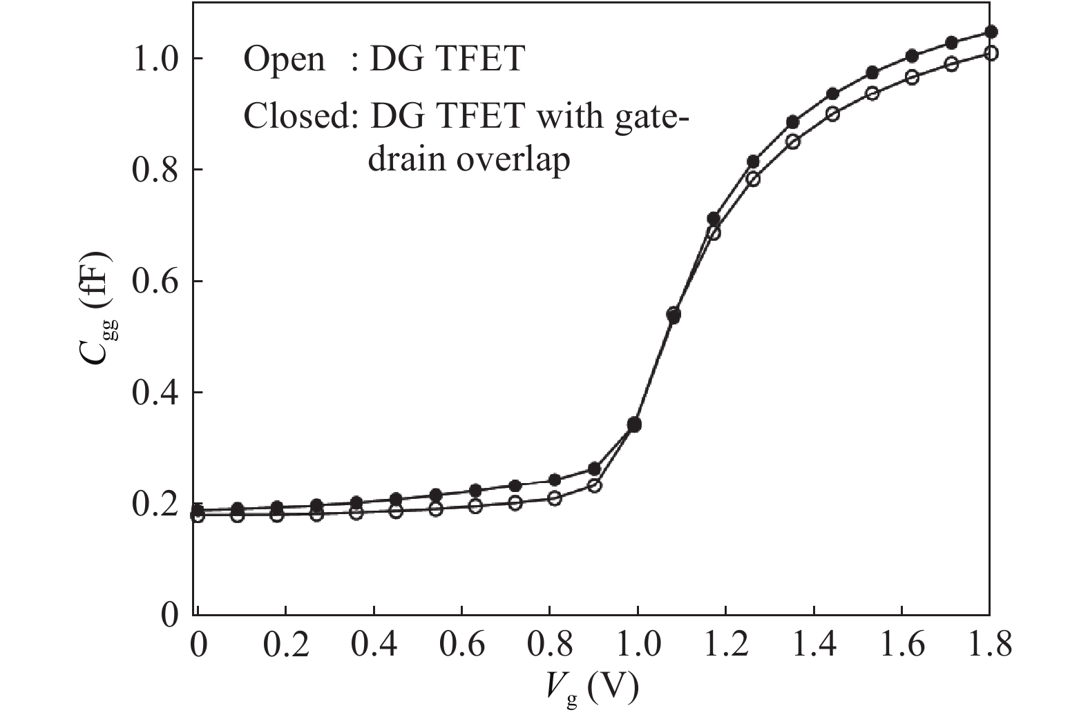
Fig. 1.
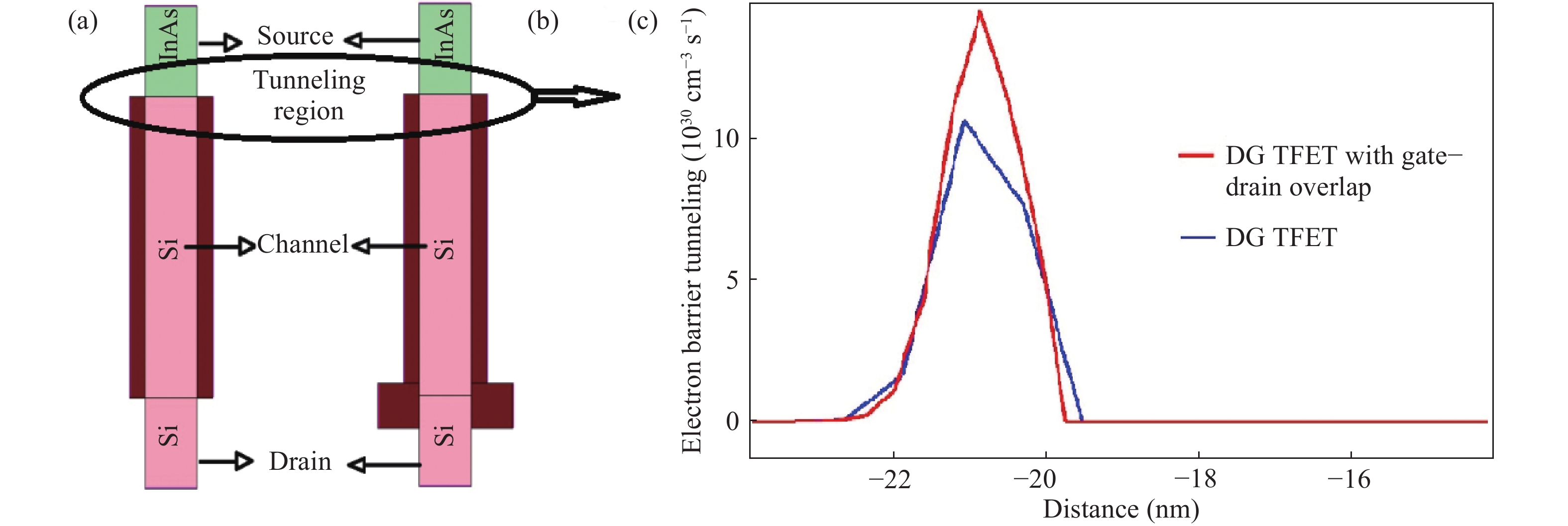
(Color online) Device structure of (a) InAs-based DG TFET and (b) DG TFET with gate–drain overlap. (c) Electron barrier tunneling for DG TFET and DG TFET with gate–drain overlap.
SEMICONDUCTOR DEVICES
Corresponding author: B. Lakshmi, Email: lakshmi.b@vit.ac.in
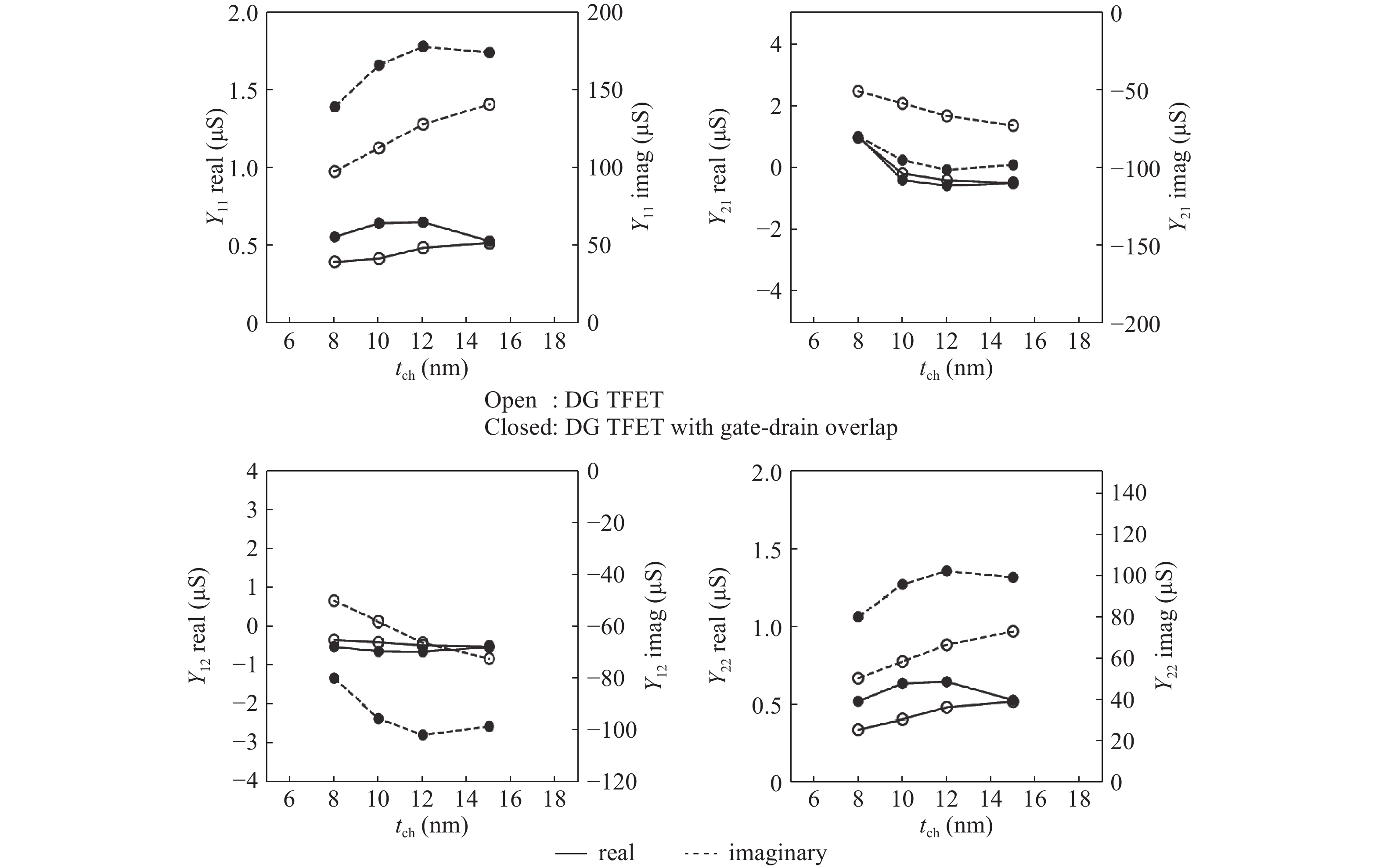
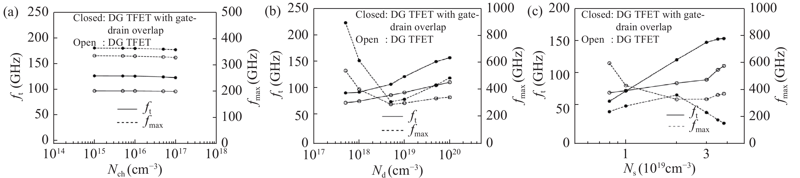
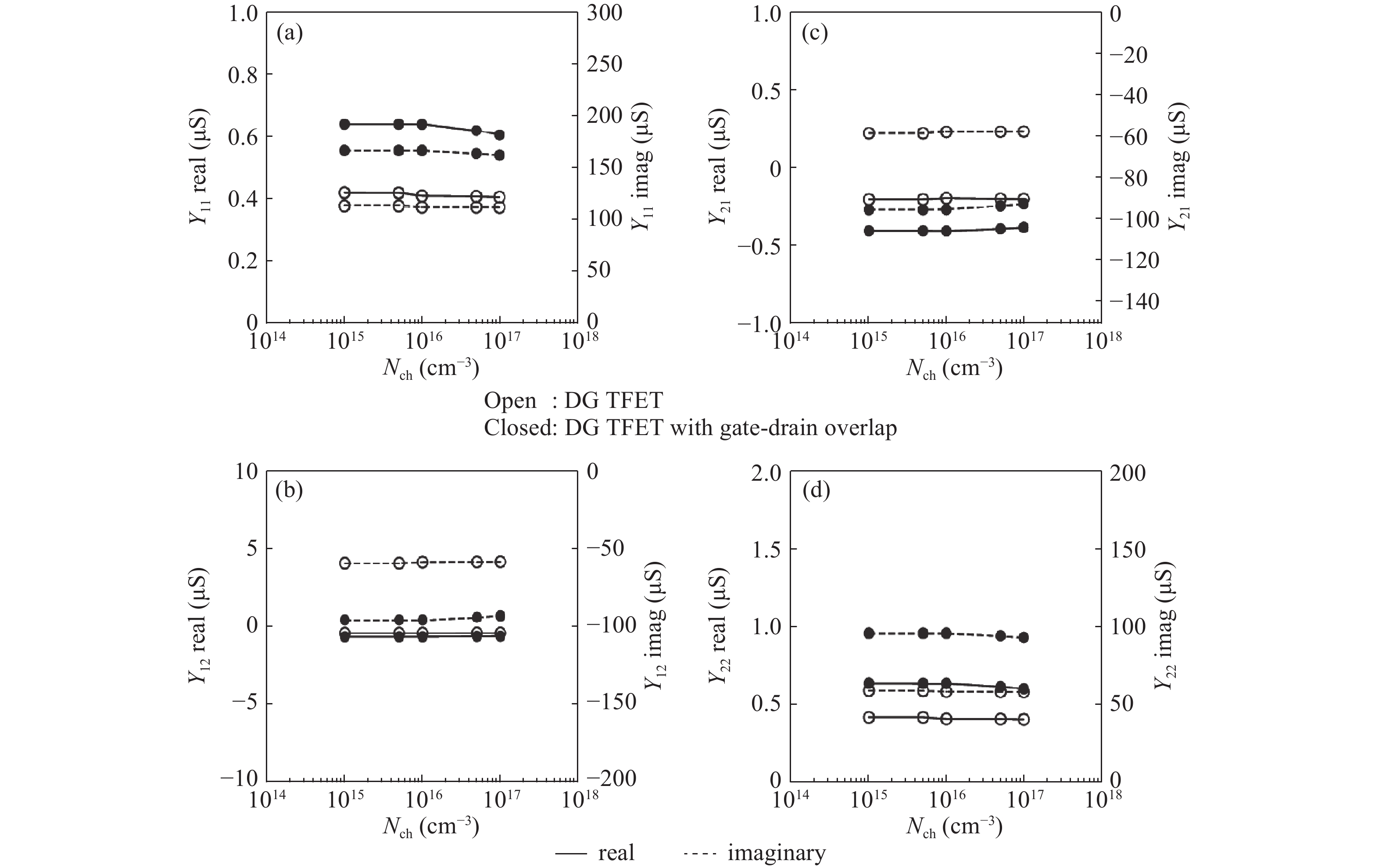
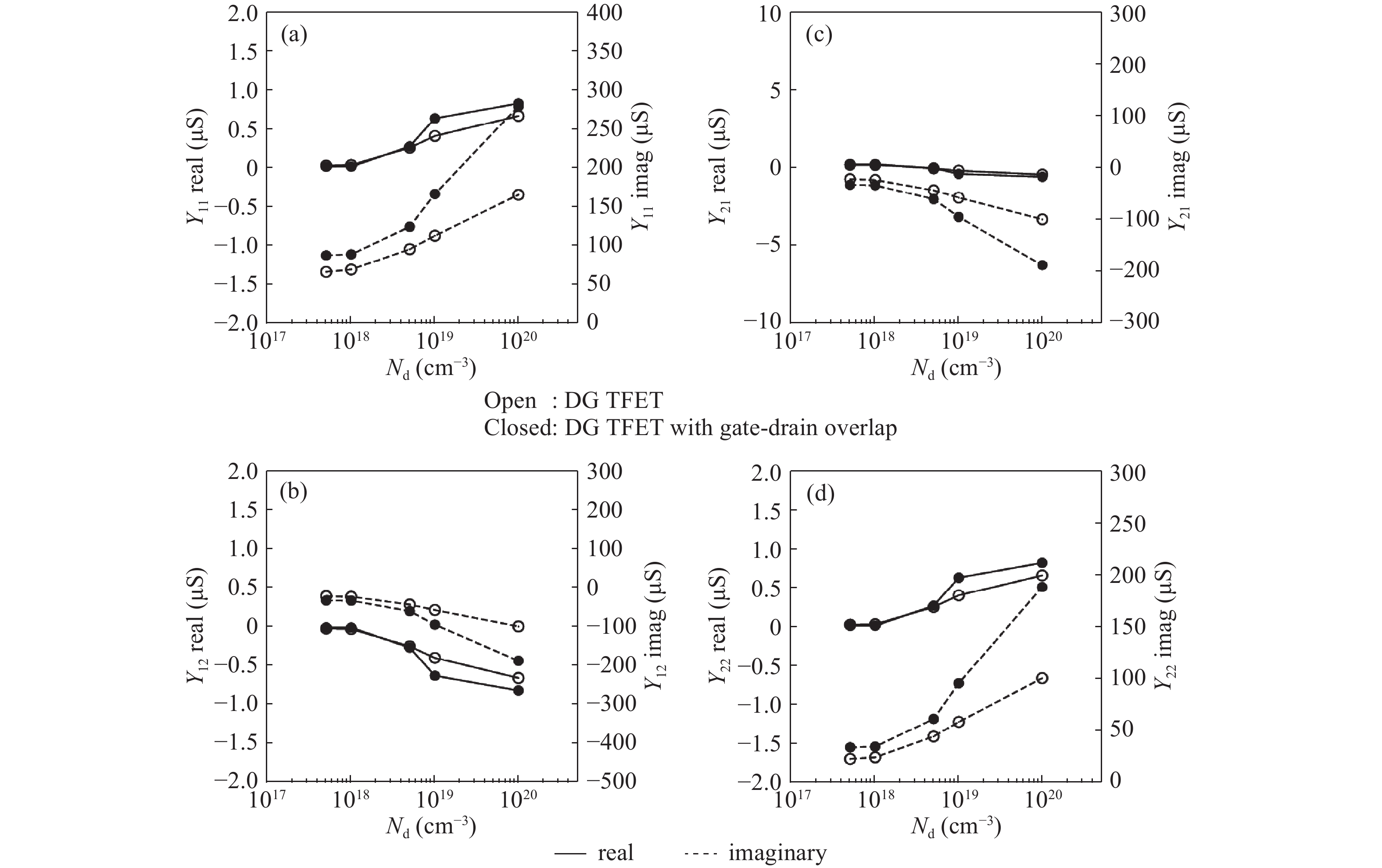
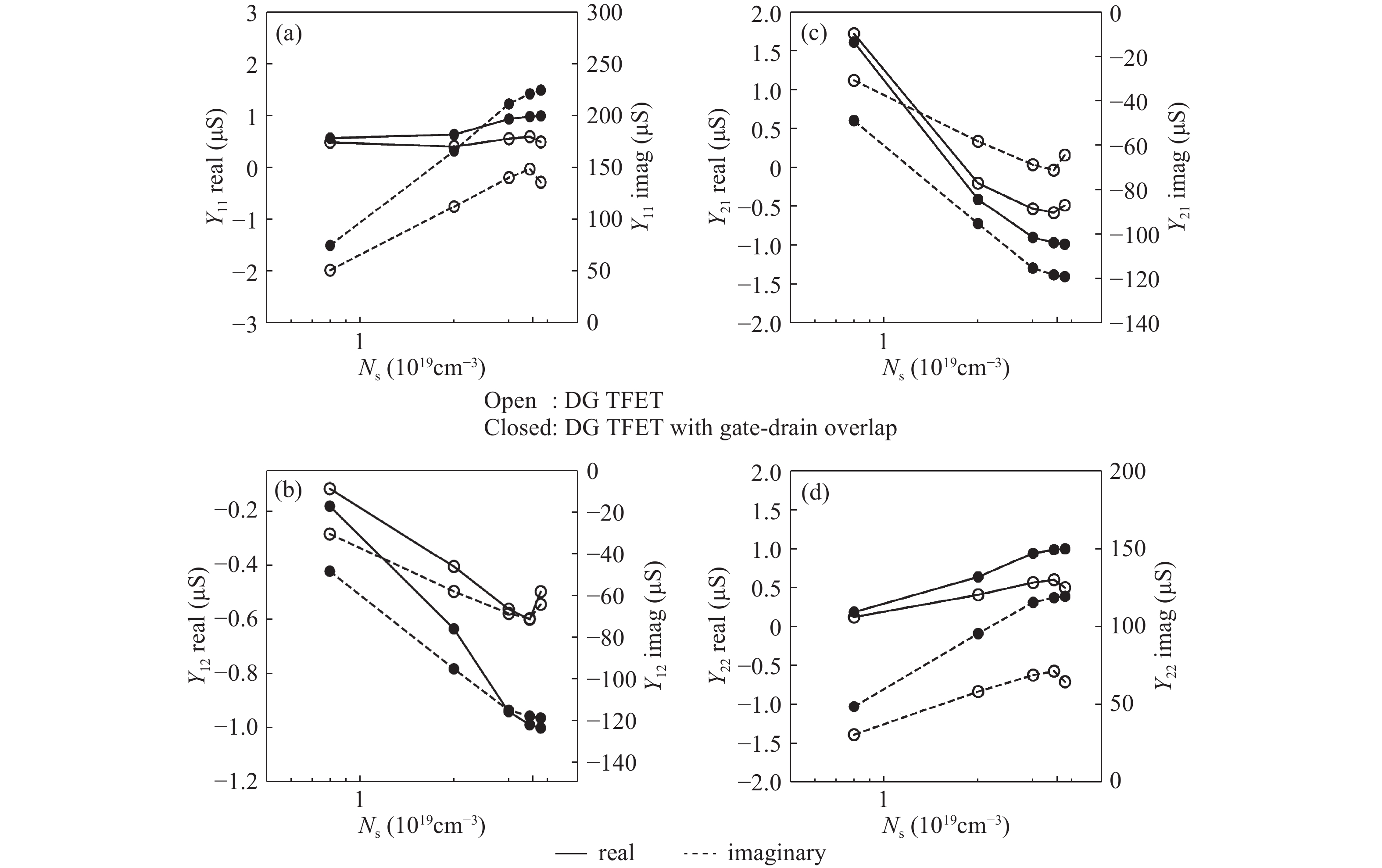
Abstract: In this paper, RF performance analysis of InAs-based double gate (DG) tunnel field effect transistors (TFETs) is investigated in both qualitative and quantitative fashion. This investigation is carried out by varying the geometrical and doping parameters of TFETs to extract various RF parameters, unity gain cut-off frequency (ft), maximum oscillation frequency (fmax), intrinsic gain and admittance (Y) parameters. An asymmetric gate oxide is introduced in the gate-drain overlap and compared with that of DG TFETs. Higher ON-current (ION) of about 0.2 mA and less leakage current (IOFF) of 29 fA is achieved for DG TFET with gate-drain overlap. Due to increase in transconductance (gm), higher ft and intrinsic gain is attained for DG TFET with gate-drain overlap. Higher fmax of 985 GHz is obtained for drain doping of 5 × 1017 cm−3 because of the reduced gate-drain capacitance (Cgd) with DG TFET with gate-drain overlap. In terms of Y-parameters, gate oxide thickness variation offers better performance due to the reduced values of Cgd. A second order numerical polynomial model is generated for all the RF responses as a function of geometrical and doping parameters. The simulation results are compared with this numerical model where the predicted values match with the simulated values.
Keywords: double gate tunnel FETs, gate-drain overlap, unity gain cut-off frequency, maximum oscillation frequency, Y-parameters, modeling
| [1] |
Zhang Q, Zhao W, A Seabaugh. Analytic expression and approach for low subthreshold-swing tunnel transistors. 63rd Device Research Conference Digest, 2005
|
| [2] |
Gupta P S, Kanungo S, Rahaman H, et al. An extremely low sub-threshold swing UTB SOI tunnel-FET structure suitable for low-power applications. Int J Appl Phys and Mathematics, 2012, 2(4): 240
|
| [3] |
Boucart K, Ionescu A M. Double-gate tunnel FET with high-k gate dielectric. IEEE Trans Electron Devices, 2007, 54(7): 172
|
| [4] |
Seabaugh A C, Zhang Q. Low-voltage tunnel transistors for beyond CMOS logic. Proc IEEE, 2010, 98(2): 2095
|
| [5] |
Verhulst A S, Sore B, Leonelli D, et al. Modeling the single-gate, double-gate, and gate-all- around tunnel field-effect transistor. J Appl Phys, 2010, 107(2): 024518 doi: 10.1063/1.3277044
|
| [6] |
Lee K F, Li Y M, Yiu C Y, et al. Characteristic optimization of single and double tunneling field effect transistors. NSTI-Nanotech, 2010, 2
|
| [7] |
Zhang L N, Chan M S, He F. The impact of device parameter variation on double gate tunneling FET and double gate MOSFET. IEEE Int Conf on Electron Devices and Solid-State Circuits, Hong Kong, China, 2010
|
| [8] |
Saurabh S, Kumar M J. Novel attributes of a dual material gate nanoscale tunnel field-effect transistor. IEEE Trans Electron Devices, 2011, 58(2): 404 doi: 10.1109/TED.2010.2093142
|
| [9] |
Boucart K, Riess W, Ionescu A M. Lateral strain profile as key technology booster for all silicon tunnel FETs. IEEE Electron Device Lett, 2009, 30(6): 656658
|
| [10] |
Abdi D B, Kumar M J. Controlling ambipolar current in tunneling FETs using overlapping gate-on-drain. J Electron Device Society, 2014, 2(6): 187 doi: 10.1109/JEDS.2014.2327626
|
| [11] |
Yoon Y J, Eun H R, Seo J H, et al. Short-channel tunneling field-effect transistor with drain-overlap and dual-metal gate structure for low-power and high-speed operations. J Nanosci and Nanotechnol, 2015, 15: 7430 doi: 10.1166/jnn.2015.11146
|
| [12] |
Madan J, Chaujar R. Gate drain-overlapped-asymmetric gate dielectric-GAA-TFET: a solution for suppressed ambipolarity and enhanced ON state behavior. Appl Phys A, 2016, 122(11)
|
| [13] |
Mookerjea S, Datta S. Comparative study of Si, Ge, InAs based steep threshold slope tunnel transistors for 0.25 V supply voltage logic applications. Device Research Conference, Santa Barbara, CA, USA, 2008.
|
| [14] |
Ahish S, Sharma D, Kuma Y B N, et al. Performance enhancement of novel InAs/Si hetero double-gate tunnel FET using gaussian doping. IEEE Trans Electron Devices, 2016, 63(1): 288 doi: 10.1109/TED.2015.2503141
|
| [15] |
Cao W, Yao C J, Jiao G F, et al. Improvement in reliability of tunneling field-effect transistor with p-n-i-n structure. IEEE Trans Electron Devices, 2011, 58(7): 2122 doi: 10.1109/TED.2011.2144987
|
| [16] |
Synopsys Sentaurus Device User Guide version J-2014.09
|
| [17] |
Ionescu A M. Tunnel field-effect transistors as energy-efficient electronic switches. Nature, 2011, 479(3): 329
|
| [18] |
Hanna A N, Fahad H M, Hussain M M. InAs/Si hetero-junction nanotube tunnel transistors. Scientific Reports, 2015, 5
|
| [19] |
Yang Y, X T, Yang L T, et al. Tunneling field-effect transistor: capacitance components and modeling. IEEE Electron Device Lett, 2010, 31(7): 752 doi: 10.1109/LED.2010.2047240
|
| [20] |
Lakshmi B, Srinivasan R. Numerical modeling of process parameters on RF metrics in FinFETs, junctionless, and gate-all-around devices. Int J Numerical Modelling: Electronic Networks, Devices and Fields, 2016, 30(5)
|
| [21] |
Montgomery D C. Design and analysis of experiments. USA: John Wiley and Sons, 2001
|
| [22] |
Lazaro A, Iniguez B. RF and noise performance of double gate and single gate SOI. Solid-State Electron, 2006, 50: 826 doi: 10.1016/j.sse.2006.03.042
|
| [23] |
Cho S, Kang IM. Design optimization of tunneling field-effect transistor based on silicon nanowire PNPN structure and its radio frequency characteristics. Current Appl Phy, 2012, 12(3): 673 doi: 10.1016/j.cap.2011.10.003
|
| [24] |
Nandi A, Saxena A K, Dasgupta S. Design and analysis of analog performance of dual-k spacer underlap N/P-FinFET at 12 nm gate length. IEEE Trans Electron Devices, 2013, 60(5): 1529 doi: 10.1109/TED.2013.2250975
|
| [25] |
Lakshmi B, Srinivasan R. Effect of structural and doping parameter variations on NQS delay, intrinsic gain and NF in Juctionless FETs. ARPN J Engineering and Appl Sci, 2015, 10(4): 1642
|
| [26] |
Cho S, Lee J S, Kim K R, et al. Analyses on small-signal parameters and radio-frequency modeling of gate-all-around tunneling field-effect transistors. IEEE Trans Electron Device, 2011, 58(12): 4164 doi: 10.1109/TED.2011.2167335
|
| [27] |
Marjani S, Hosseini S E. Radio-frequency small-signal model of heterogate-dielectric p–n–p–n tunneling field effect transistor including charge conservation capacitance and substrate parameters. J Appl Phys, 2015, 118: 095708 doi: 10.1063/1.4929361
|
| [28] |
Landau S, Crc H. A handbook of statistical analyses using SPSS. New York: Landau, Sabine, and Hall Crc, 2004
|
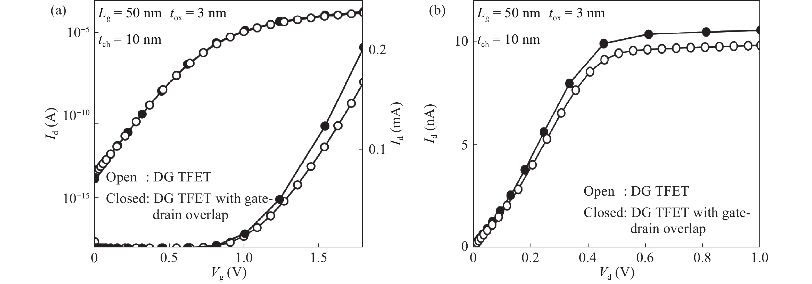
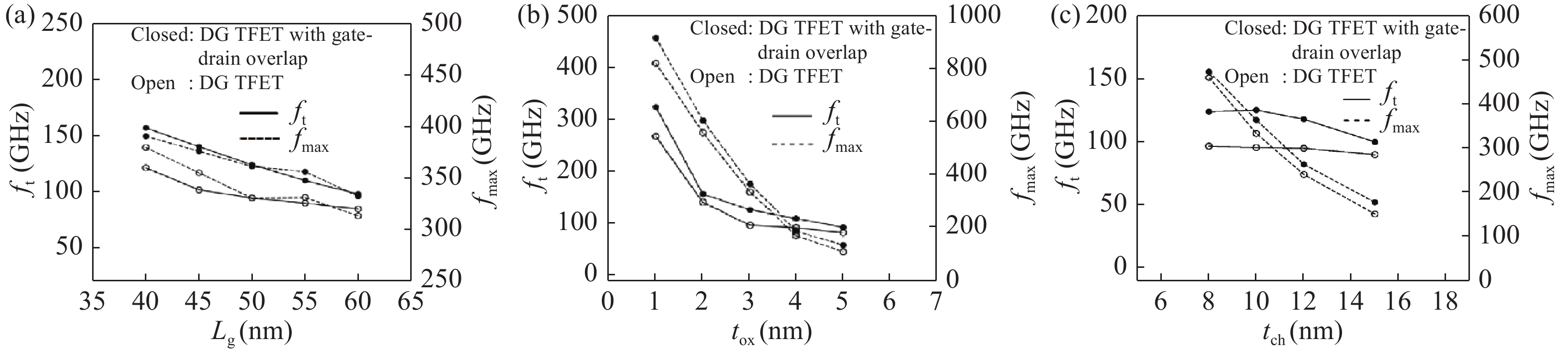
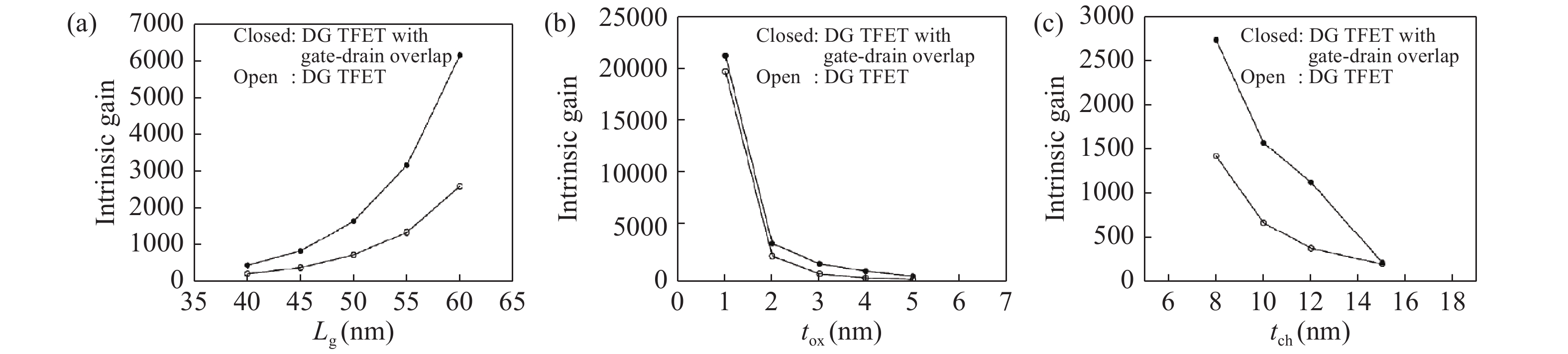
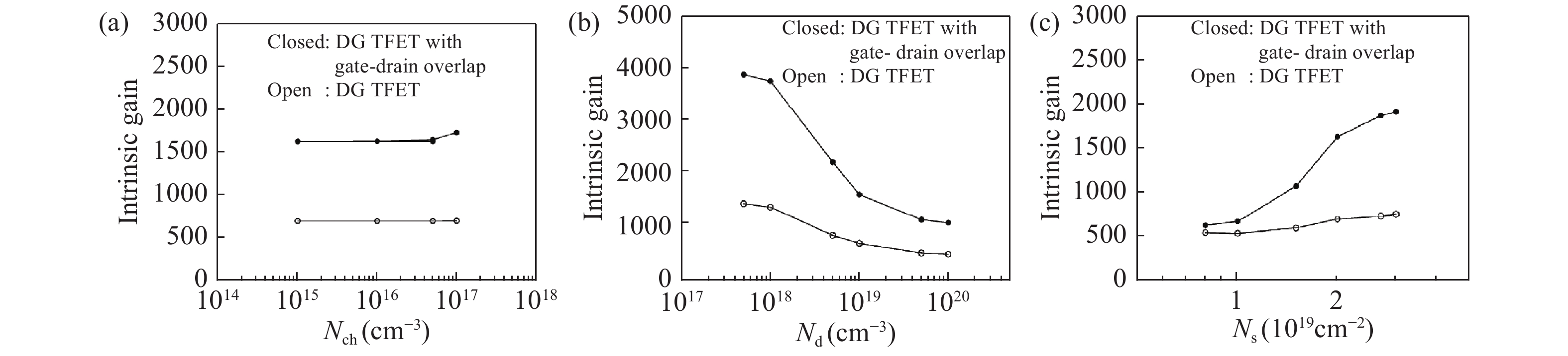
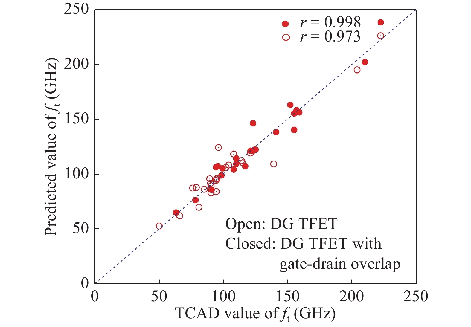
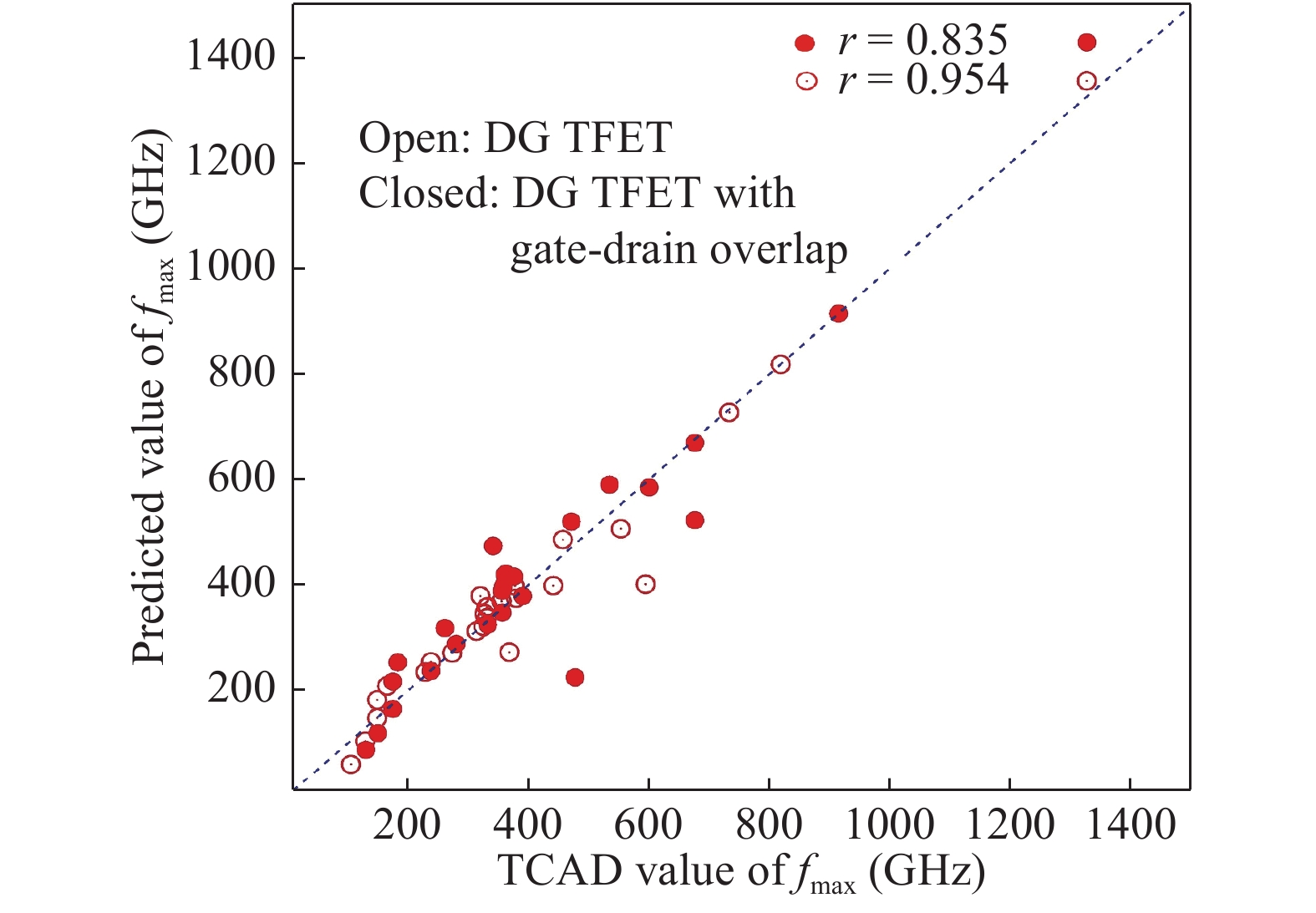
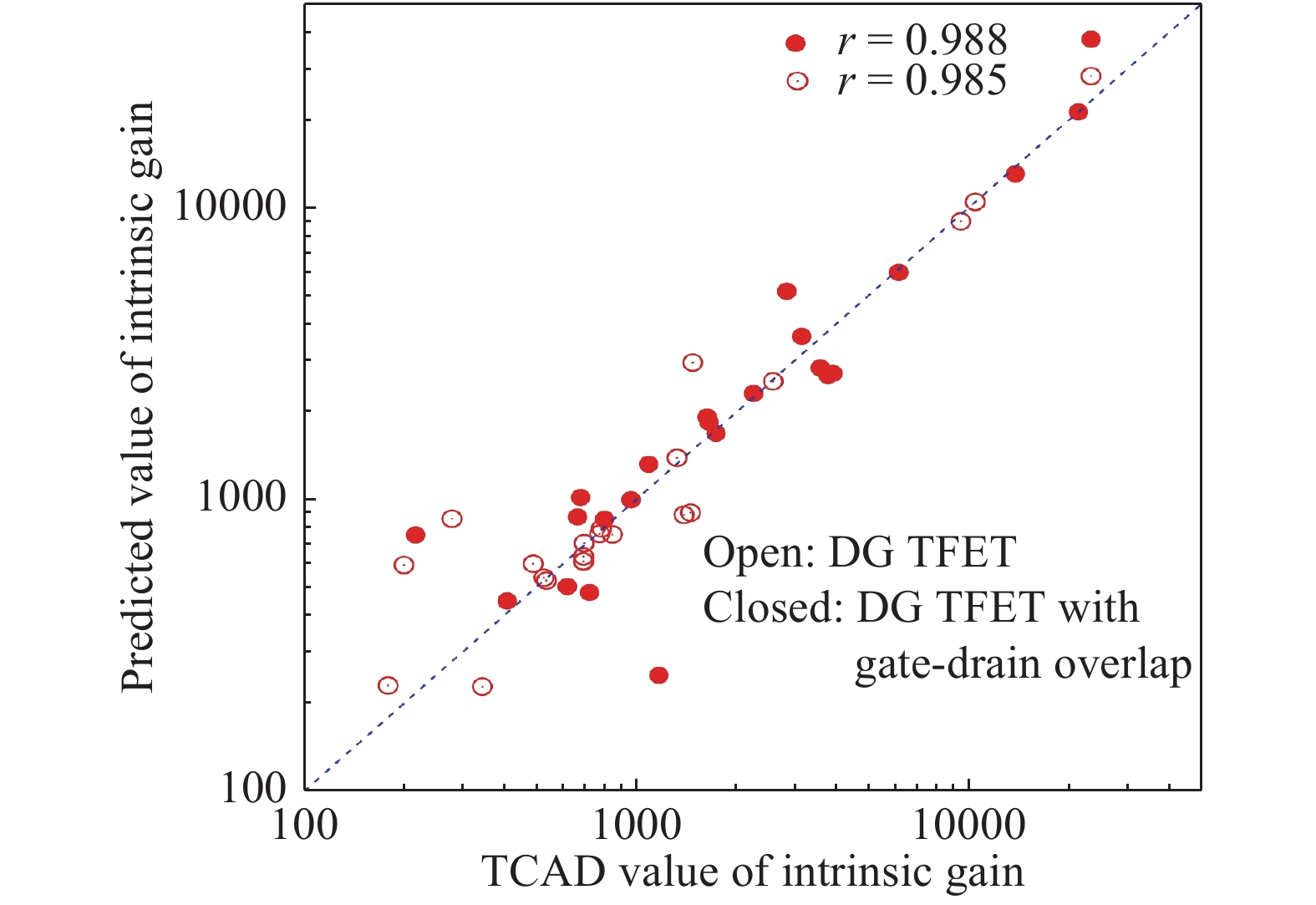
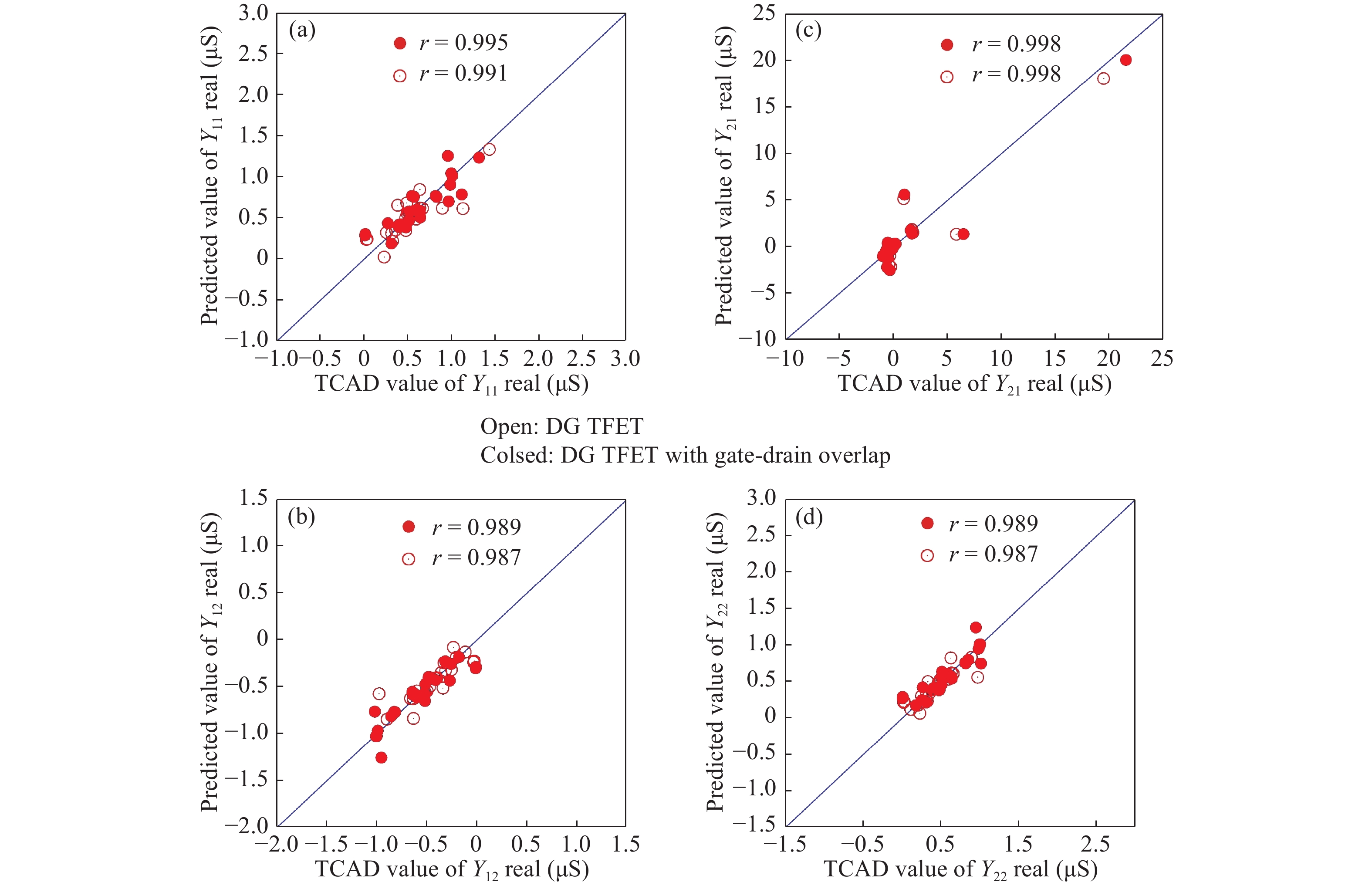
Table 1. Parameter space of DG TFETs with and without gate–drain overlap.
| Parameters | Nominal value | Range of values | ||
| Gate length Lg (nm) | 50 | 40–60 | ||
| Gate oxide thickness tox (nm) | 3 | 1–5 | ||
| Channel thickness tch (nm) | 10 | 8–15 | ||
| Channel doping concentration Nch (cm−3) | 1 × 10¹⁶ | 1 × 10¹⁵–1 × 10¹⁷ | ||
| Drain doping concentration Nd (cm−3) | 1 × 10¹⁹ | 5 × 10¹⁷–1 × 10²⁰ | ||
| Source doping concentration Ns (cm−3) | 2 × 10¹⁹ | 8 × 10¹⁸–4 × 10¹⁹ |
 DownLoad: CSV
| [1] |
Zhang Q, Zhao W, A Seabaugh. Analytic expression and approach for low subthreshold-swing tunnel transistors. 63rd Device Research Conference Digest, 2005
|
| [2] |
Gupta P S, Kanungo S, Rahaman H, et al. An extremely low sub-threshold swing UTB SOI tunnel-FET structure suitable for low-power applications. Int J Appl Phys and Mathematics, 2012, 2(4): 240
|
| [3] |
Boucart K, Ionescu A M. Double-gate tunnel FET with high-k gate dielectric. IEEE Trans Electron Devices, 2007, 54(7): 172
|
| [4] |
Seabaugh A C, Zhang Q. Low-voltage tunnel transistors for beyond CMOS logic. Proc IEEE, 2010, 98(2): 2095
|
| [5] |
Verhulst A S, Sore B, Leonelli D, et al. Modeling the single-gate, double-gate, and gate-all- around tunnel field-effect transistor. J Appl Phys, 2010, 107(2): 024518 doi: 10.1063/1.3277044
|
| [6] |
Lee K F, Li Y M, Yiu C Y, et al. Characteristic optimization of single and double tunneling field effect transistors. NSTI-Nanotech, 2010, 2
|
| [7] |
Zhang L N, Chan M S, He F. The impact of device parameter variation on double gate tunneling FET and double gate MOSFET. IEEE Int Conf on Electron Devices and Solid-State Circuits, Hong Kong, China, 2010
|
| [8] |
Saurabh S, Kumar M J. Novel attributes of a dual material gate nanoscale tunnel field-effect transistor. IEEE Trans Electron Devices, 2011, 58(2): 404 doi: 10.1109/TED.2010.2093142
|
| [9] |
Boucart K, Riess W, Ionescu A M. Lateral strain profile as key technology booster for all silicon tunnel FETs. IEEE Electron Device Lett, 2009, 30(6): 656658
|
| [10] |
Abdi D B, Kumar M J. Controlling ambipolar current in tunneling FETs using overlapping gate-on-drain. J Electron Device Society, 2014, 2(6): 187 doi: 10.1109/JEDS.2014.2327626
|
| [11] |
Yoon Y J, Eun H R, Seo J H, et al. Short-channel tunneling field-effect transistor with drain-overlap and dual-metal gate structure for low-power and high-speed operations. J Nanosci and Nanotechnol, 2015, 15: 7430 doi: 10.1166/jnn.2015.11146
|
| [12] |
Madan J, Chaujar R. Gate drain-overlapped-asymmetric gate dielectric-GAA-TFET: a solution for suppressed ambipolarity and enhanced ON state behavior. Appl Phys A, 2016, 122(11)
|
| [13] |
Mookerjea S, Datta S. Comparative study of Si, Ge, InAs based steep threshold slope tunnel transistors for 0.25 V supply voltage logic applications. Device Research Conference, Santa Barbara, CA, USA, 2008.
|
| [14] |
Ahish S, Sharma D, Kuma Y B N, et al. Performance enhancement of novel InAs/Si hetero double-gate tunnel FET using gaussian doping. IEEE Trans Electron Devices, 2016, 63(1): 288 doi: 10.1109/TED.2015.2503141
|
| [15] |
Cao W, Yao C J, Jiao G F, et al. Improvement in reliability of tunneling field-effect transistor with p-n-i-n structure. IEEE Trans Electron Devices, 2011, 58(7): 2122 doi: 10.1109/TED.2011.2144987
|
| [16] |
Synopsys Sentaurus Device User Guide version J-2014.09
|
| [17] |
Ionescu A M. Tunnel field-effect transistors as energy-efficient electronic switches. Nature, 2011, 479(3): 329
|
| [18] |
Hanna A N, Fahad H M, Hussain M M. InAs/Si hetero-junction nanotube tunnel transistors. Scientific Reports, 2015, 5
|
| [19] |
Yang Y, X T, Yang L T, et al. Tunneling field-effect transistor: capacitance components and modeling. IEEE Electron Device Lett, 2010, 31(7): 752 doi: 10.1109/LED.2010.2047240
|
| [20] |
Lakshmi B, Srinivasan R. Numerical modeling of process parameters on RF metrics in FinFETs, junctionless, and gate-all-around devices. Int J Numerical Modelling: Electronic Networks, Devices and Fields, 2016, 30(5)
|
| [21] |
Montgomery D C. Design and analysis of experiments. USA: John Wiley and Sons, 2001
|
| [22] |
Lazaro A, Iniguez B. RF and noise performance of double gate and single gate SOI. Solid-State Electron, 2006, 50: 826 doi: 10.1016/j.sse.2006.03.042
|
| [23] |
Cho S, Kang IM. Design optimization of tunneling field-effect transistor based on silicon nanowire PNPN structure and its radio frequency characteristics. Current Appl Phy, 2012, 12(3): 673 doi: 10.1016/j.cap.2011.10.003
|
| [24] |
Nandi A, Saxena A K, Dasgupta S. Design and analysis of analog performance of dual-k spacer underlap N/P-FinFET at 12 nm gate length. IEEE Trans Electron Devices, 2013, 60(5): 1529 doi: 10.1109/TED.2013.2250975
|
| [25] |
Lakshmi B, Srinivasan R. Effect of structural and doping parameter variations on NQS delay, intrinsic gain and NF in Juctionless FETs. ARPN J Engineering and Appl Sci, 2015, 10(4): 1642
|
| [26] |
Cho S, Lee J S, Kim K R, et al. Analyses on small-signal parameters and radio-frequency modeling of gate-all-around tunneling field-effect transistors. IEEE Trans Electron Device, 2011, 58(12): 4164 doi: 10.1109/TED.2011.2167335
|
| [27] |
Marjani S, Hosseini S E. Radio-frequency small-signal model of heterogate-dielectric p–n–p–n tunneling field effect transistor including charge conservation capacitance and substrate parameters. J Appl Phys, 2015, 118: 095708 doi: 10.1063/1.4929361
|
| [28] |
Landau S, Crc H. A handbook of statistical analyses using SPSS. New York: Landau, Sabine, and Hall Crc, 2004
|


Article views: 4233 Times PDF downloads: 67 Times Cited by: 0 Times
Received: 10 August 2017 Revised: 28 October 2017 Online: Uncorrected proof: 25 January 2018Accepted Manuscript: 18 April 2018Published: 01 May 2018
| Citation: |
S. Poorvasha, B. Lakshmi. Investigation and statistical modeling of InAs-based double gate tunnel FETs for RF performance enhancement[J]. Journal of Semiconductors, 2018, 39(5): 054001. doi: 10.1088/1674-4926/39/5/054001
****
S. Poorvasha, B. Lakshmi. Investigation and statistical modeling of InAs-based double gate tunnel FETs for RF performance enhancement[J]. J. Semicond., 2018, 39(5): 054001. doi: 10.1088/1674-4926/39/5/054001.

|
| [1] |
Zhang Q, Zhao W, A Seabaugh. Analytic expression and approach for low subthreshold-swing tunnel transistors. 63rd Device Research Conference Digest, 2005
|
| [2] |
Gupta P S, Kanungo S, Rahaman H, et al. An extremely low sub-threshold swing UTB SOI tunnel-FET structure suitable for low-power applications. Int J Appl Phys and Mathematics, 2012, 2(4): 240
|
| [3] |
Boucart K, Ionescu A M. Double-gate tunnel FET with high-k gate dielectric. IEEE Trans Electron Devices, 2007, 54(7): 172
|
| [4] |
Seabaugh A C, Zhang Q. Low-voltage tunnel transistors for beyond CMOS logic. Proc IEEE, 2010, 98(2): 2095
|
| [5] |
Verhulst A S, Sore B, Leonelli D, et al. Modeling the single-gate, double-gate, and gate-all- around tunnel field-effect transistor. J Appl Phys, 2010, 107(2): 024518 doi: 10.1063/1.3277044
|
| [6] |
Lee K F, Li Y M, Yiu C Y, et al. Characteristic optimization of single and double tunneling field effect transistors. NSTI-Nanotech, 2010, 2
|
| [7] |
Zhang L N, Chan M S, He F. The impact of device parameter variation on double gate tunneling FET and double gate MOSFET. IEEE Int Conf on Electron Devices and Solid-State Circuits, Hong Kong, China, 2010
|
| [8] |
Saurabh S, Kumar M J. Novel attributes of a dual material gate nanoscale tunnel field-effect transistor. IEEE Trans Electron Devices, 2011, 58(2): 404 doi: 10.1109/TED.2010.2093142
|
| [9] |
Boucart K, Riess W, Ionescu A M. Lateral strain profile as key technology booster for all silicon tunnel FETs. IEEE Electron Device Lett, 2009, 30(6): 656658
|
| [10] |
Abdi D B, Kumar M J. Controlling ambipolar current in tunneling FETs using overlapping gate-on-drain. J Electron Device Society, 2014, 2(6): 187 doi: 10.1109/JEDS.2014.2327626
|
| [11] |
Yoon Y J, Eun H R, Seo J H, et al. Short-channel tunneling field-effect transistor with drain-overlap and dual-metal gate structure for low-power and high-speed operations. J Nanosci and Nanotechnol, 2015, 15: 7430 doi: 10.1166/jnn.2015.11146
|
| [12] |
Madan J, Chaujar R. Gate drain-overlapped-asymmetric gate dielectric-GAA-TFET: a solution for suppressed ambipolarity and enhanced ON state behavior. Appl Phys A, 2016, 122(11)
|
| [13] |
Mookerjea S, Datta S. Comparative study of Si, Ge, InAs based steep threshold slope tunnel transistors for 0.25 V supply voltage logic applications. Device Research Conference, Santa Barbara, CA, USA, 2008.
|
| [14] |
Ahish S, Sharma D, Kuma Y B N, et al. Performance enhancement of novel InAs/Si hetero double-gate tunnel FET using gaussian doping. IEEE Trans Electron Devices, 2016, 63(1): 288 doi: 10.1109/TED.2015.2503141
|
| [15] |
Cao W, Yao C J, Jiao G F, et al. Improvement in reliability of tunneling field-effect transistor with p-n-i-n structure. IEEE Trans Electron Devices, 2011, 58(7): 2122 doi: 10.1109/TED.2011.2144987
|
| [16] |
Synopsys Sentaurus Device User Guide version J-2014.09
|
| [17] |
Ionescu A M. Tunnel field-effect transistors as energy-efficient electronic switches. Nature, 2011, 479(3): 329
|
| [18] |
Hanna A N, Fahad H M, Hussain M M. InAs/Si hetero-junction nanotube tunnel transistors. Scientific Reports, 2015, 5
|
| [19] |
Yang Y, X T, Yang L T, et al. Tunneling field-effect transistor: capacitance components and modeling. IEEE Electron Device Lett, 2010, 31(7): 752 doi: 10.1109/LED.2010.2047240
|
| [20] |
Lakshmi B, Srinivasan R. Numerical modeling of process parameters on RF metrics in FinFETs, junctionless, and gate-all-around devices. Int J Numerical Modelling: Electronic Networks, Devices and Fields, 2016, 30(5)
|
| [21] |
Montgomery D C. Design and analysis of experiments. USA: John Wiley and Sons, 2001
|
| [22] |
Lazaro A, Iniguez B. RF and noise performance of double gate and single gate SOI. Solid-State Electron, 2006, 50: 826 doi: 10.1016/j.sse.2006.03.042
|
| [23] |
Cho S, Kang IM. Design optimization of tunneling field-effect transistor based on silicon nanowire PNPN structure and its radio frequency characteristics. Current Appl Phy, 2012, 12(3): 673 doi: 10.1016/j.cap.2011.10.003
|
| [24] |
Nandi A, Saxena A K, Dasgupta S. Design and analysis of analog performance of dual-k spacer underlap N/P-FinFET at 12 nm gate length. IEEE Trans Electron Devices, 2013, 60(5): 1529 doi: 10.1109/TED.2013.2250975
|
| [25] |
Lakshmi B, Srinivasan R. Effect of structural and doping parameter variations on NQS delay, intrinsic gain and NF in Juctionless FETs. ARPN J Engineering and Appl Sci, 2015, 10(4): 1642
|
| [26] |
Cho S, Lee J S, Kim K R, et al. Analyses on small-signal parameters and radio-frequency modeling of gate-all-around tunneling field-effect transistors. IEEE Trans Electron Device, 2011, 58(12): 4164 doi: 10.1109/TED.2011.2167335
|
| [27] |
Marjani S, Hosseini S E. Radio-frequency small-signal model of heterogate-dielectric p–n–p–n tunneling field effect transistor including charge conservation capacitance and substrate parameters. J Appl Phys, 2015, 118: 095708 doi: 10.1063/1.4929361
|
| [28] |
Landau S, Crc H. A handbook of statistical analyses using SPSS. New York: Landau, Sabine, and Hall Crc, 2004
|

 WeChat ID
Journal of Semiconductors © 2017 All Rights Reserved 京ICP备05085259号-2