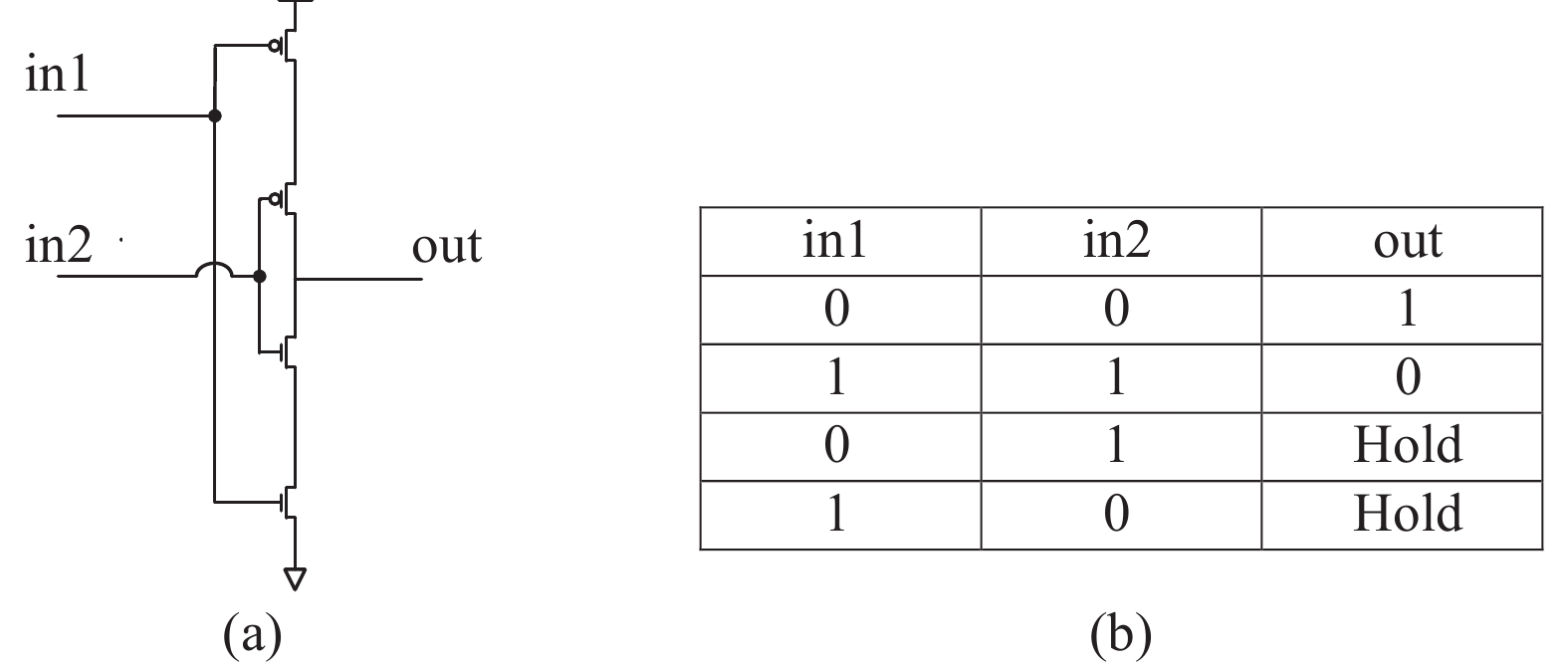
J. Semicond. > 2018, Volume 39 > Issue 5 > 055003

SEMICONDUCTOR INTEGRATED CIRCUITS

An advanced SEU tolerant latch based on error detection

Hui Xu1, 3, Jianwei Zhu2, , Xiaoping Lu2 and Jingzhao Li2

+ Author Affiliations

 Corresponding author: Jianwei Zhu, E-mail address: zhujw68@163.com

DOI: 10.1088/1674-4926/39/5/055003

PDF

Turn off MathJax

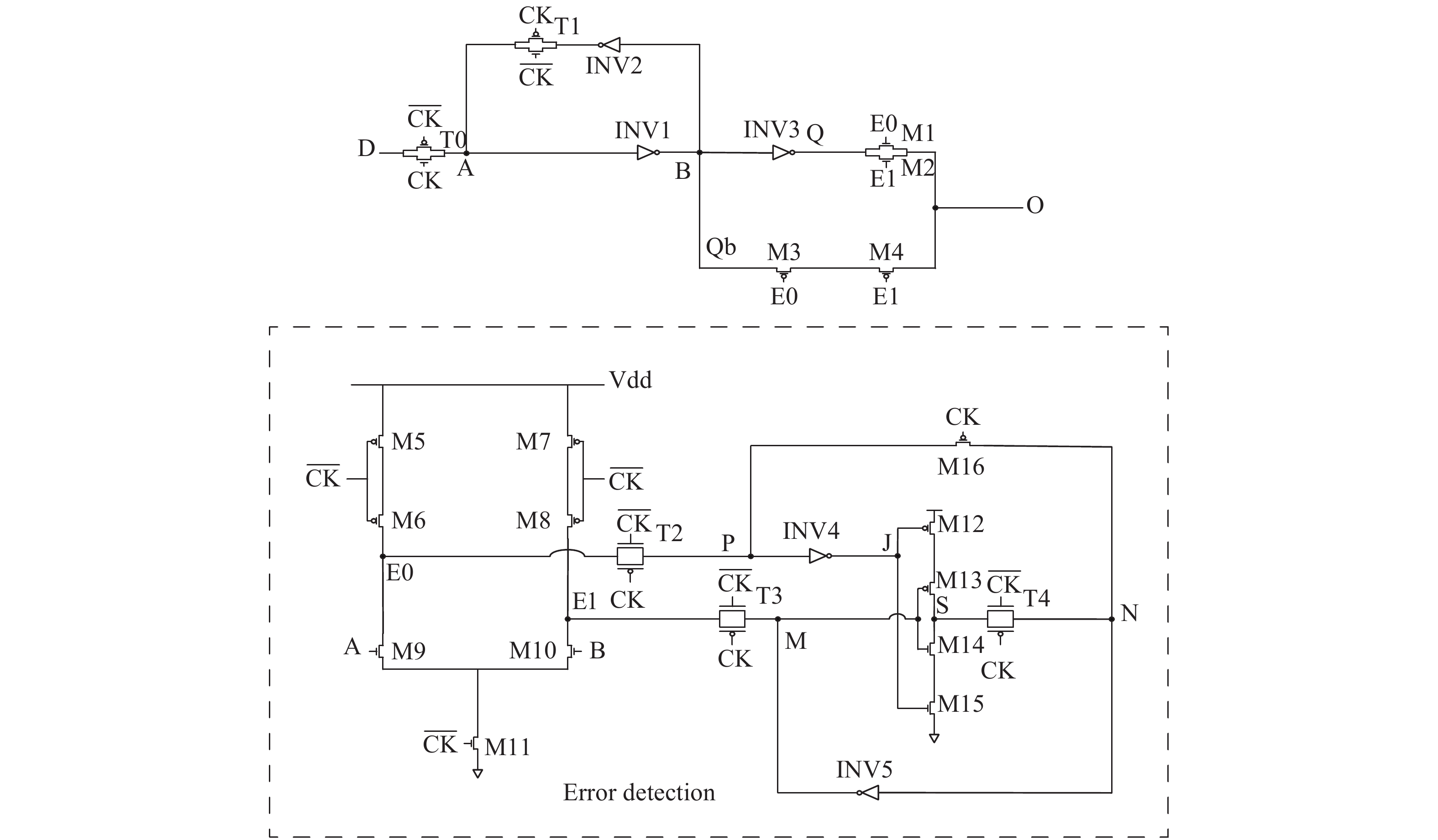
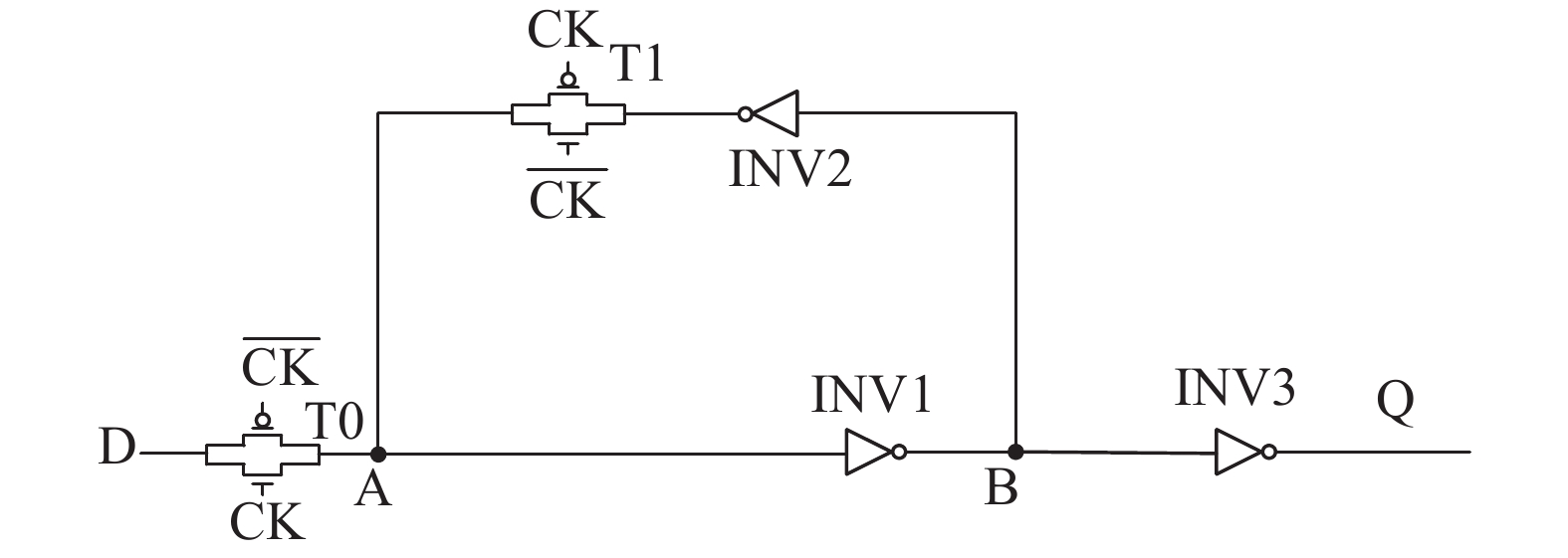
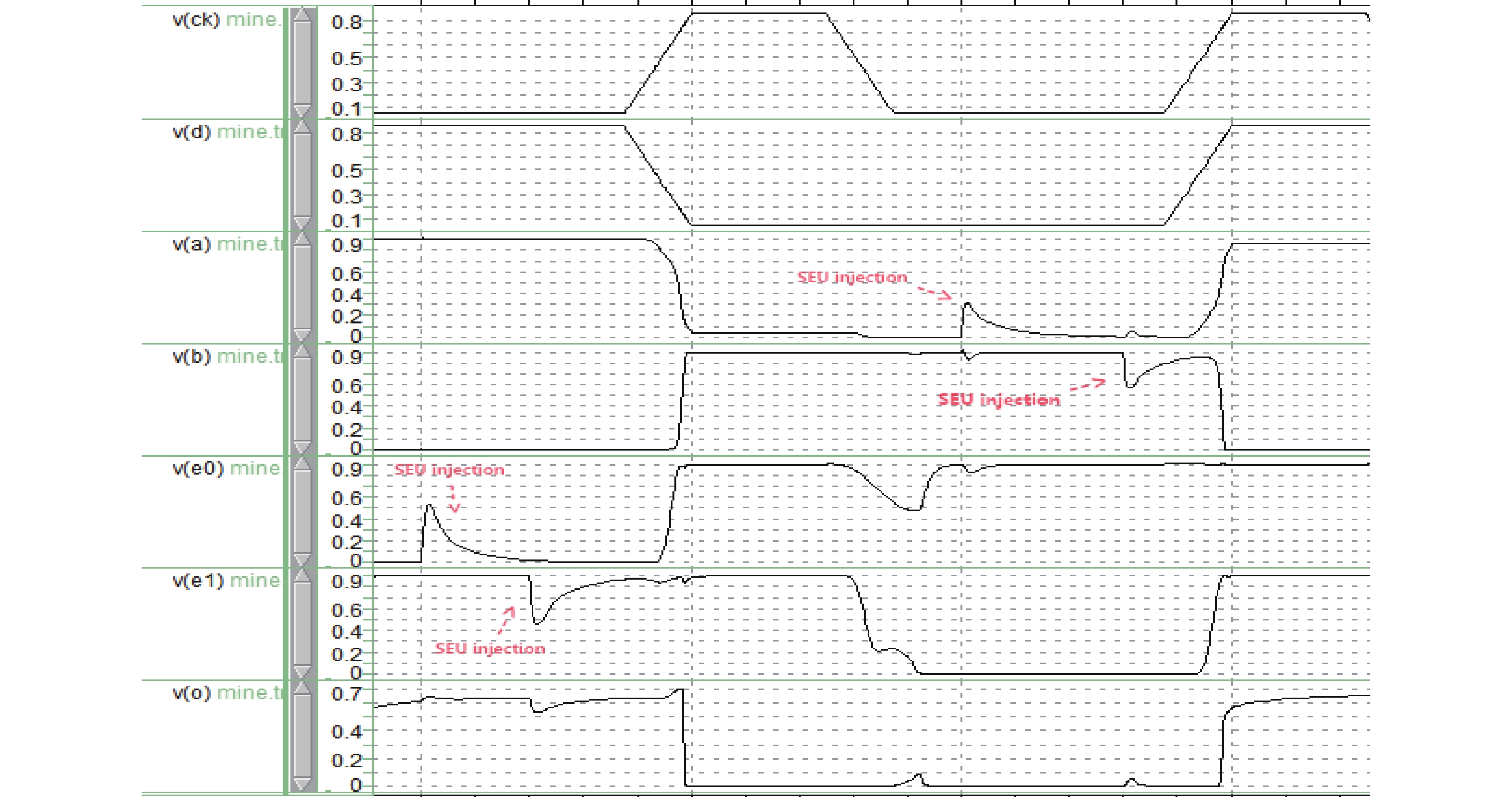
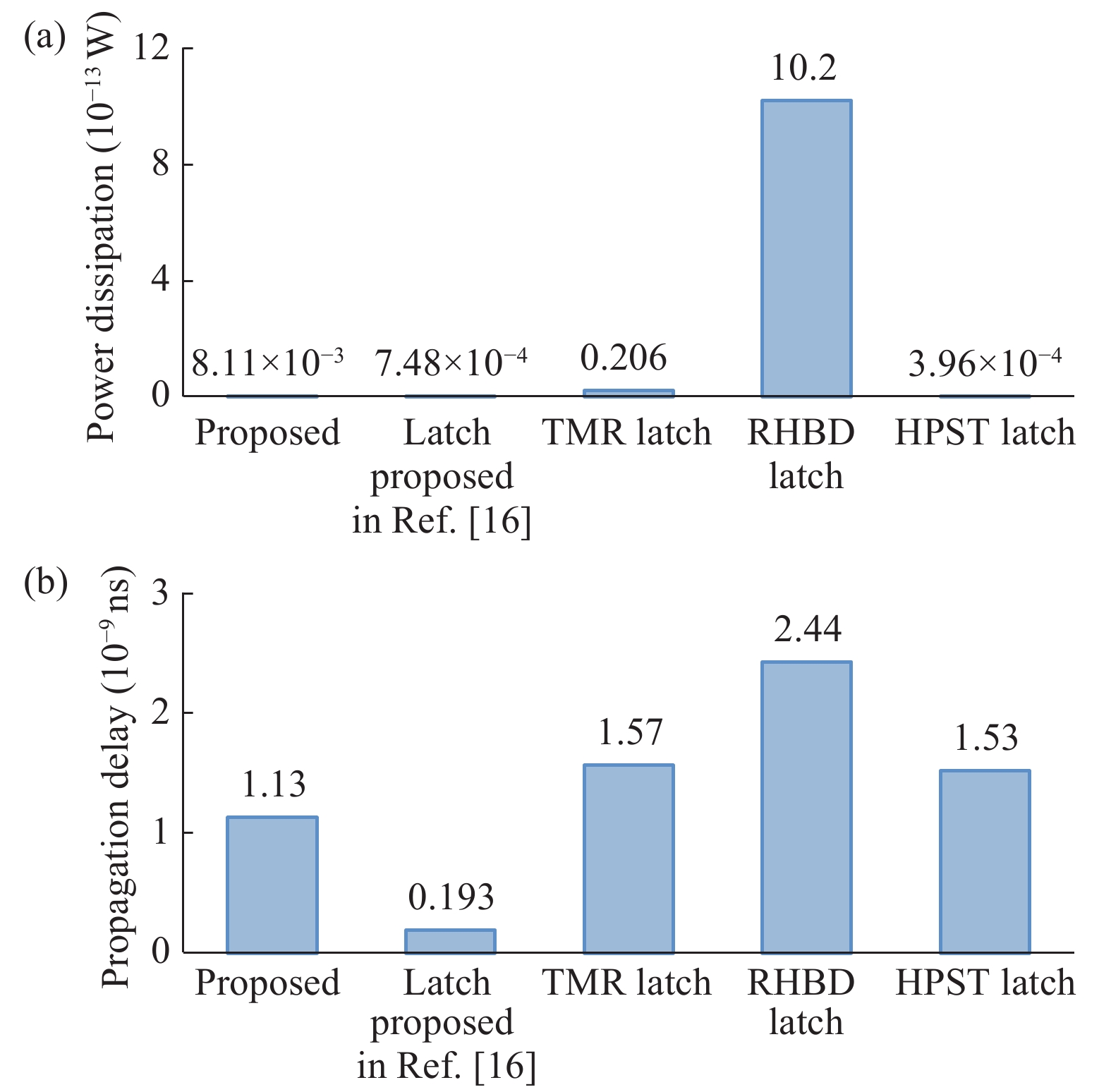
Abstract: This paper proposes a latch that can mitigate SEUs via an error detection circuit. The error detection circuit is hardened by a C-element and a stacked PMOS. In the hold state, a particle strikes the latch or the error detection circuit may cause a fault logic state of the circuit. The error detection circuit can detect the upset node in the latch and the fault output will be corrected. The upset node in the error detection circuit can be corrected by the C-element. The power dissipation and propagation delay of the proposed latch are analyzed by HSPICE simulations. The proposed latch consumes about 77.5% less energy and 33.1% less propagation delay than the triple modular redundancy (TMR) latch. Simulation results demonstrate that the proposed latch can mitigate SEU effectively.

Key words: single event upset (SEU)latcherror detectionstacked

With the development of semiconductor technology, the size of the integrated circuit is reducing and the supply voltage is getting lower and lower, which results in increased soft errors caused by radiation. This leads to increased susceptibility of SRAM, latches and flip-flops to single event upset (SEU)[1, 2]. The energetic particle striking the circuit causes the transistor to generate electrons and holes. The generated holes and electrons are accumulated in a drain node, leading to an upset[3]. When the particle charge is beyond an expected range, a soft error will happen. The expected range is called critical charge. In other words, the higher the critical charge, the higher tolerant capability to soft error. The Semiconductor Industry Association Roadmap has identified SEU effects as the major threat to reliable operation of electronic systems in the future[4, 5]. Therefore, many schemes designed to tolerate errors have been presented, such as radiation-hardening-by-design (RHBD) techniques. RHBD techniques include spatial redundancy and temporal redundancy. Spatial redundancy techniques, such as triple modular redundancy (TMR) and dual interlocked storage cell (DICE) designs increase the reliability of the system at varying levels of performance penalties[59].

Fig. 1 gives the structure of a standard static latch, the latch is very sensitive to high energetic particles and easily causes an SEU. In the hold state, assume that the clock signal ck is 0, when an energetic particle strikes node A or node B, the logic state will upset and the fault value will be saved via the feedback until the next logic value is written.

Figure  1.  The standard static latch.

This paper proposes a new latch to mitigate SEUs, the latch includes an error detection circuit and a C-element. The error detection circuit produces signals when an error occurs in the latch. The produced signals were used to control the latch, thus the fault value will be blocked and the right value will be output. The C-element will correct the fault value in the error detection circuit if an SEU occurs.

C-element is a famous design which can block SEU induced soft errors, the basic structure of C-element consists of 2 PMOS and 2 NMOS. Fig. 2 gives the structure of C-element and its true table. When giving the two inputs the same value, the output will get an inverse value. If two inputs are of different value, the output will hold the current state. State holding characteristics can block SEU from occurring at the internal nodes with minimal hardware overhead[10].

Figure  2.  (a) C-element. (b) C-element truth table.

For mitigating the vulnerability to single node strikes, we propose a stacked transistor. The stacked transistor hardening technique has superior SEU tolerant ability[1113]. The stacked transistor approach isolates the sensitive node connected to the two off-state transistors, if only one gets hit, the other one will prevent the critical node from flipping[14].

Fig. 3 gives the structure of the proposed latch: the latch consists of two parts, the static latch circuit and the error detection circuit. In the static latch circuit, it has two transmission gates (T0, T1) and three inverters (INV1, INV2, INV3). Node A and Node B are connected to the corresponding location of the error detection circuit, respectively. There is a C-element and two stacked PMOS (M6, M8) in the error detection circuit. The error indication signal E0 and E1 are connected to the static latch circuit to control the state of the transmission path.

Figure  3.  The proposed SEU tolerant latch.

When the clock (CK) is high (the inverted signal CKB is low), the transmission gate T0 is turned on, T1, T2, T3 and T4 are in an off-state. We assume that the input D is logic 0, so node A is logic 0, node B is logic 1, node Q is logic 0 and node Qb is logic 1. In the error detection circuit, NMOS M9 is turned off and NMOS M10 is turned on. PMOS M5, M6, M7 and M8 are turned on due to CKB is low, NMOS M11 is turned off, node E0 and node E1 are connected to Vdd, so the value of E0 and E1 are logic 1. The output O is logic 0, is equal to node Q and the input D. When the clock (CK) is low (CKB is high), the transmission gate T0 is turned off, T1 is turned on, the latch is in a hold phase. In the error detection circuit, T2, T3 and T4 are turned on, PMOS M16 is turned on, PMOS M5, M6, M7 and M8 are in an off-state. NMOS M11 is turned on, because node B is logic 1, NMOS M10 is turned on, node E1 is connected to the ground and the value of E1 turns to be logic 0. E0 remains logic 1 because node A is logic 0 and NMOS M9 is in an off-state. Because the transmission gates T2, T3 and T4 are turned on, node P is logic 1 is equal to node E0, node J is logic 0. Node M is logic 0 is equal to node E1. After the signal passes through the C-element, node S and node N are logic 1. The signal will feed back node E0 and E1 via the feedback loop. Node E0 and node E1 are hardened.

It is assumed that node A has an SEU, node A holds a fault value 1 and node B holds a fault value 0 accordingly (node Qb is equal to node B is logic 0). So NMOS M10 is turned off and NMOS M9 is turned on. Node E0 is connected to the ground, and the value of E0 will be logic 0. Node E1 remains logic 0 because its charge has been put over before the SEU occurs. In the static latch circuit, NMOS M1 and NMOS M2 are turned off, PMOS M3 and PMOS M4 are turned on, the output O is equal to the node Qb is the right logic 0. Node B is similar to node A. It is assumed that an SEU occurs on node E0, node E0 holds a fault value 0, node J holds a fault value 1 accordingly, node M remains logic 0, as mentioned in section 2, the output of the C-element S will hold the current state. So, node S remains logic 1. The error will soon be corrected through the feedback loop. Node E1 is similar to node E0. In summary, the proposed latch can mitigate SEUs on node A, node B, node E0 and node E1.

When a particle strikes the error detection circuit. PMOS M5 and PMOS M7 may be turned on, the Vdd signal will influence the state of E0 or E1. The two staked PMOS M6 and M8 will prevent this case happening. If one PMOS was struck and turned on, the other one will block the signal. So, node E0 and node E1 are hardened again.

The clock uncertainty may impact this scheme due to extra switches being necessary for the scheme. However, the latch proposed in Ref. [21] includes 5 transmission gates controlled by the clock signal, it did not make any comment about the clock uncertainty’s impact to the scheme. Triple Modular Redundancy is the most common SEU hardened technology. The TMR latch in Ref. [22] has 6 transmission gates, the 6 transmission gates are controlled by the clock signal. There are more clock distributions in the latch, while the scheme can work well. It is the same in Ref. [5]. The proposed SEU tolerant latch in this paper has 5 transmission gates controlled by the clock signal, the number is similar to those in Refs. [21, 22, 5]. Generally, the clock uncertainty makes very little impact on the latch proposed in this paper.

HSPICE was used to simulate the proposed latch, HSPICE uses advanced Predictive Technology Model (PTM). The nano-scale Integration and Modeling (NIMO) group of Arizona State University invented PTM. As an evolution of traditional Berkeley Predictive Technology Model (BPTM), PTM of bulk CMOS is successfully generated for 130 to 32 nm technology nodes[10]. PTM is more physical, scalable, and continuous over technology generations and suitable for emerging variability and reliability issues[15]. To simulate the circuits, a 32 nm technology model is used and the supply voltage is 0.9 V.

The SEU injection method is used to simulate high-energy particle striking. Fig. 4 shows the experimental results when an SEU was injected at nodes A, B, E0 and E1. It describes CK (the clock signal), the input signal D and signals on node A, B, E0 and E1. It is clearly in Fig. 4, the output O holds the same value of input D. Node A holds the same value of input D and node B holds the invert value. In the hold state, if node A or node E0 has an SEU, the output O is almost unaffected. If an SEU occurs on node B or node E1, the output O generates only a little glitch, which can be ignored. In general, the proposed latch has SEU tolerant capability on node A, node B, node E0 and node E1.

Figure  4.  (Color online) The experimental results when an SEU was injected at node A, node B, node E0, node E1.

The proposed latch is compared with other SEU tolerant latches in two terms: power and propagation delay. It is clearly in Fig. 5, although the latch proposed in the paper did not get the lowest power and propagation delay, it achieves lower power and propagation delay than the RHBD latch[10] and the TMR latch[1720]. The proposed latch achieves lower propagation delay than the HPST latch proposed in Ref. [21]. Although the latch proposed in Ref. [16] introduces lower power and propagation delay, it cannot mitigate SEUs on node E0 and node E1, which will result in incorrect output.

Figure  5.  (Color online) (a) Power dissipation. (b) Propagation delay.

This paper proposes a new latch that can tolerate SEUs. Through the error detection circuit, the latch can get indication signals and a fault on the error detection circuit can be corrected via a C-element. With comparison of other schemes in power and propagation delay, the proposed latch works well. Via the SEU injection experiment, it is obvious that the proposed latch is superior to other latches in SEU tolerant.


[1]
Karnik T, Hazucha P. Characterization of soft errors caused by single event upsets in CMOS processes. IEEE Trans Depend Secure Comput, 2004, 1(2): 128 doi: 10.1109/TDSC.2004.14
[2]
Schrimpf R D, Warren K M, Weller R A, et al. Reliability and radiation effects in IC technologies. IEEE International Reliability Physics Symposium, 2008: 97
[3]
Ueno H, Namba K. Construction of a soft error (SEU) hardened latch with high critical charge. IEEE International Symposium on Defect and Fault Tolerance in VLSI and Nanotechnology Systems, 2016: 27
[4]
The international technology roadmap for semiconductors. [Online]. Available: http://www.itrs.net/Links/2001ITRS/ Design.pdf
[5]
Wang H B, Li Y Q, Chen L, et al. An SEU-tolerant DICE latch design with feedback transistors. IEEE Trans Nucl Sci, 2015, 62(2): 548 doi: 10.1109/TNS.2015.2399019
[6]
Nicolaidis M. Design for soft error mitigation. IEEE Trans Device Mater Reliab, 2005, 5: 405 doi: 10.1109/TDMR.2005.855790
[7]
Pontes J, Calazans N, Vivet P. Adding temporal redundancy to delay insensitive codes to mitigate single event effects. IEEE International Symposium on Asynchronous Circuits and Systems, 2012: 142
[8]
Carmichael C, Fuller E, Blain P, et al. SEU mitigation techniques for Virtex FPGAs in space applications. Proc Military and Aerospace Programmable Logic Devices Int Conf, 1999: C2
[9]
Calin T, Nicolaidis M, Velazco R. Upset hardened memory design for submicron CMOS technology. IEEE Trans Nucl Sci, 1996, 43(6): 2874 doi: 10.1109/23.556880
[10]
Huang Z F, Liang H G. A novel radiation hardened by design latch. J Semicond, 2009, 30(3): 035007 doi: 10.1088/1674-4926/30/3/035007
[11]
Makihara A, Yamaguchi T, Asai H, et al. Optimization for SEU/SET immunity on 0.15 μm fully depleted CMOS/SOI digital logic devices. IEEE Trans Nucl Sci, 2006, 53(6): 3422 doi: 10.1109/TNS.2006.885166
[12]
Rodbell K P, Heidel D F, Pellish J A, et al. 32 and 45 nm radiation-hardened-by-design (RHBD) SOI latches. IEEE Trans Nucl Sci, 2011, 58(6): 2702 doi: 10.1109/TNS.2011.2171715
[13]
Kauppila J S, Loveless T D, Quinn R C, et al. Utilizing device stacking for area efficient hardened SOI flip-flop designs. IEEE International Reliability Physics Symposium, 2014: SE.4.1
[14]
Wang H B, Chen L, Liu R, et al. An area efficient stacked latch design tolerant to SEU in 28 nm FDSOI technology. IEEE Trans Nucl Sci, 2016, 63(6): 3003 doi: 10.1109/TNS.2016.2627003
[15]
Zhao W, Cao Y. New generation of predictive technology model for sub-45 nm early design exploration. IEEE Trans Electron Devices, 2006, 53(11): 2816 doi: 10.1109/TED.2006.884077
[16]
She X, Li N, Tong J. SEU tolerant latch based on error detection. IEEE Trans Nucl Sci, 2012, 59(1): 211 doi: 10.1109/TNS.2011.2178265
[17]
Oliveira R, Jagirdar A, Chakraborty T J. A TMR scheme for SEU mitigation in scan flip-flops. Proc 8th Int Symp Qual Electron Des, 2007: 905
[18]
Iturbe X, Azkarate M, Martinez I, et al. A novel SEU, MBU and SHE handling strategy for xilinx virtex-4 FPGAs. Proc Int Conf Field Program Logic Appl, 2009: 569
[19]
Tanoue S, Ishida T, Ichinomiya Y, et al. A novel states recovery technique for the TMR softcore processor. Proc Int Conf Field Program Logic Appl, 2009: 543
[20]
Stroud C E. Reliability of majority voting based VLSI fault-tolerant circuits. IEEE Trans VLSI Syst, 1994, 2: 516 doi: 10.1109/92.335020
[21]
Huang Z. A high performance SEU-tolerant latch for nanoscale CMOS technology. J Electron Test, 2015, 31(4): 1
[22]
Rajaei R, Tabandeh M, Rashidian B. Single event upset immune latch circuit design using C-element. IEEE 9th International Conference on ASIC (ASICON), 2011: 252
Fig. 1.  The standard static latch.

Fig. 2.  (a) C-element. (b) C-element truth table.

Fig. 3.  The proposed SEU tolerant latch.

Fig. 4.  (Color online) The experimental results when an SEU was injected at node A, node B, node E0, node E1.

Fig. 5.  (Color online) (a) Power dissipation. (b) Propagation delay.

[1]
Karnik T, Hazucha P. Characterization of soft errors caused by single event upsets in CMOS processes. IEEE Trans Depend Secure Comput, 2004, 1(2): 128 doi: 10.1109/TDSC.2004.14
[2]
Schrimpf R D, Warren K M, Weller R A, et al. Reliability and radiation effects in IC technologies. IEEE International Reliability Physics Symposium, 2008: 97
[3]
Ueno H, Namba K. Construction of a soft error (SEU) hardened latch with high critical charge. IEEE International Symposium on Defect and Fault Tolerance in VLSI and Nanotechnology Systems, 2016: 27
[4]
The international technology roadmap for semiconductors. [Online]. Available: http://www.itrs.net/Links/2001ITRS/ Design.pdf
[5]
Wang H B, Li Y Q, Chen L, et al. An SEU-tolerant DICE latch design with feedback transistors. IEEE Trans Nucl Sci, 2015, 62(2): 548 doi: 10.1109/TNS.2015.2399019
[6]
Nicolaidis M. Design for soft error mitigation. IEEE Trans Device Mater Reliab, 2005, 5: 405 doi: 10.1109/TDMR.2005.855790
[7]
Pontes J, Calazans N, Vivet P. Adding temporal redundancy to delay insensitive codes to mitigate single event effects. IEEE International Symposium on Asynchronous Circuits and Systems, 2012: 142
[8]
Carmichael C, Fuller E, Blain P, et al. SEU mitigation techniques for Virtex FPGAs in space applications. Proc Military and Aerospace Programmable Logic Devices Int Conf, 1999: C2
[9]
Calin T, Nicolaidis M, Velazco R. Upset hardened memory design for submicron CMOS technology. IEEE Trans Nucl Sci, 1996, 43(6): 2874 doi: 10.1109/23.556880
[10]
Huang Z F, Liang H G. A novel radiation hardened by design latch. J Semicond, 2009, 30(3): 035007 doi: 10.1088/1674-4926/30/3/035007
[11]
Makihara A, Yamaguchi T, Asai H, et al. Optimization for SEU/SET immunity on 0.15 μm fully depleted CMOS/SOI digital logic devices. IEEE Trans Nucl Sci, 2006, 53(6): 3422 doi: 10.1109/TNS.2006.885166
[12]
Rodbell K P, Heidel D F, Pellish J A, et al. 32 and 45 nm radiation-hardened-by-design (RHBD) SOI latches. IEEE Trans Nucl Sci, 2011, 58(6): 2702 doi: 10.1109/TNS.2011.2171715
[13]
Kauppila J S, Loveless T D, Quinn R C, et al. Utilizing device stacking for area efficient hardened SOI flip-flop designs. IEEE International Reliability Physics Symposium, 2014: SE.4.1
[14]
Wang H B, Chen L, Liu R, et al. An area efficient stacked latch design tolerant to SEU in 28 nm FDSOI technology. IEEE Trans Nucl Sci, 2016, 63(6): 3003 doi: 10.1109/TNS.2016.2627003
[15]
Zhao W, Cao Y. New generation of predictive technology model for sub-45 nm early design exploration. IEEE Trans Electron Devices, 2006, 53(11): 2816 doi: 10.1109/TED.2006.884077
[16]
She X, Li N, Tong J. SEU tolerant latch based on error detection. IEEE Trans Nucl Sci, 2012, 59(1): 211 doi: 10.1109/TNS.2011.2178265
[17]
Oliveira R, Jagirdar A, Chakraborty T J. A TMR scheme for SEU mitigation in scan flip-flops. Proc 8th Int Symp Qual Electron Des, 2007: 905
[18]
Iturbe X, Azkarate M, Martinez I, et al. A novel SEU, MBU and SHE handling strategy for xilinx virtex-4 FPGAs. Proc Int Conf Field Program Logic Appl, 2009: 569
[19]
Tanoue S, Ishida T, Ichinomiya Y, et al. A novel states recovery technique for the TMR softcore processor. Proc Int Conf Field Program Logic Appl, 2009: 543
[20]
Stroud C E. Reliability of majority voting based VLSI fault-tolerant circuits. IEEE Trans VLSI Syst, 1994, 2: 516 doi: 10.1109/92.335020
[21]
Huang Z. A high performance SEU-tolerant latch for nanoscale CMOS technology. J Electron Test, 2015, 31(4): 1
[22]
Rajaei R, Tabandeh M, Rashidian B. Single event upset immune latch circuit design using C-element. IEEE 9th International Conference on ASIC (ASICON), 2011: 252
1

A 0.1–1.5 GHz multi-octave quadruple-stacked CMOS power amplifier

Shizhe Wei, Haifeng Wu, Qian Lin, Mingzhe Zhang

Journal of Semiconductors, 2020, 41(6): 062401. doi: 10.1088/1674-4926/41/6/062401

2

Engineering in-plane silicon nanowire springs for highly stretchable electronics

Zhaoguo Xue, Taige Dong, Zhimin Zhu, Yaolong Zhao, Ying Sun, et al.

Journal of Semiconductors, 2018, 39(1): 011001. doi: 10.1088/1674-4926/39/1/011001

3

Detection of lead ions with AlGaAs/InGaAs pseudomorphic high electron mobility transistor

Jiqiang Niu, Yang Zhang, Min Guan, Chengyan Wang, Lijie Cui, et al.

Journal of Semiconductors, 2016, 37(11): 114003. doi: 10.1088/1674-4926/37/11/114003

4

Simulation study on single event burnout in linear doping buffer layer engineered power VDMOSFET

Jia Yunpeng, Su Hongyuan, Jin Rui, Hu Dongqing, Wu Yu, et al.

Journal of Semiconductors, 2016, 37(2): 024008. doi: 10.1088/1674-4926/37/2/024008

5

Impacts of test factors on heavy ion single event multiple-cell upsets in nanometer-scale SRAM

Yinhong Luo, Fengqi Zhang, Hongxia Guo, Yao Xiao, Wen Zhao, et al.

Journal of Semiconductors, 2015, 36(11): 114009. doi: 10.1088/1674-4926/36/11/114009

6

A four-interleaving HBD SRAM cell based on dual DICE for multiple node collection mitigation

Lin Liu, Suge Yue, Shijin Lu

Journal of Semiconductors, 2015, 36(11): 115007. doi: 10.1088/1674-4926/36/11/115007

7

Single event soft error in advanced integrated circuit

Yuanfu Zhao, Suge Yue, Xinyuan Zhao, Shijin Lu, Qiang Bian, et al.

Journal of Semiconductors, 2015, 36(11): 111001. doi: 10.1088/1674-4926/36/11/111001

8

Modeling and simulation of single-event effect in CMOS circuit

Suge Yue, Xiaolin Zhang, Yuanfu Zhao, Lin Liu

Journal of Semiconductors, 2015, 36(11): 111002. doi: 10.1088/1674-4926/36/11/111002

9

Analytical modeling and simulation of germanium single gate silicon on insulator TFET

T. S. Arun Samuel, N. B. Balamurugan

Journal of Semiconductors, 2014, 35(3): 034002. doi: 10.1088/1674-4926/35/3/034002

10

Impact of temperature on single event upset measurement by heavy ions in SRAM devices

Tianqi Liu, Chao Geng, Zhangang Zhang, Fazhan Zhao, Song Gu, et al.

Journal of Semiconductors, 2014, 35(8): 084008. doi: 10.1088/1674-4926/35/8/084008

11

Laser SEU sensitivity mapping of deep submicron CMOS SRAM

Yongtao Yu, Guoqiang Feng, Rui Chen, Jianwei Han

Journal of Semiconductors, 2014, 35(6): 064011. doi: 10.1088/1674-4926/35/6/064011

12

An SEU-hardened latch with a triple-interlocked structure

Li Yuanqing, Yao Suying, Xu Jiangtao, Gao Jing

Journal of Semiconductors, 2012, 33(8): 085002. doi: 10.1088/1674-4926/33/8/085002

13

SRAM single event upset calculation and test using protons in the secondary beam in the BEPC

Wang Yuanming, Guo Hongxia, Zhang Fengqi, Zhang Keying, Chen Wei, et al.

Journal of Semiconductors, 2011, 32(9): 092001. doi: 10.1088/1674-4926/32/9/092001

14

A signal processing method for the friction-based endpoint detection system of a CMP process

Xu Chi, Guo Dongming, Jin Zhuji, Kang Renke

Journal of Semiconductors, 2010, 31(12): 126002. doi: 10.1088/1674-4926/31/12/126002

15

Thermal analysis and test for single concentrator solar cells

Cui Min, Chen Nuofu, Yang Xiaoli, Wang Yu, Bai Yiming, et al.

Journal of Semiconductors, 2009, 30(4): 044011. doi: 10.1088/1674-4926/30/4/044011

16

Formation of stacked ruthenium nanocrystals embedded in SiO2 for nonvolatile memory applications

Mao Ping, Zhang Zhigang, Pan Liyang, Xu Jun, Chen Peiyi, et al.

Journal of Semiconductors, 2009, 30(9): 093003. doi: 10.1088/1674-4926/30/9/093003

17

Fabrication and Numerical Simulation of a Micromachined Contact Cantilever RF-MEMS Switch

Sun Jianhai, Cui Dafu, Xiao Jiang

Chinese Journal of Semiconductors , 2006, 27(2): 309-312.

18

Single Mode Operation of Short-Cavity Quantum Cascade Lasers

Liu Fengqi, Guo Yu, Li Lu, Shao Ye, Liu Junqi, et al.

Chinese Journal of Semiconductors , 2006, 27(4): 679-682.

19

12Gb/s 0.25μm CMOS Low-Power 1∶4 Demultiplexer

Ding Jingfeng, Wang Zhigong, Zhu En, Zhang Li, Wang Gui, et al.

Chinese Journal of Semiconductors , 2006, 27(1): 19-23.

20

20Gb/s 1∶2 Demultiplexer in 0.18μm CMOS

Chinese Journal of Semiconductors , 2005, 26(10): 1881-1885.

1. Pannu, N., Prakash, N.R. Modeling and simulation of low power single event upset-resilient SRAM cell. Analog Integrated Circuits and Signal Processing, 2025, 122(2): 19. doi:10.1007/s10470-025-02326-y
2. Xu, H., Liu, C., Ma, R. et al. Hardened latch designs based on the characteristic of transistor for mitigating multiple-node-upsets in harsh radiation environments. Microelectronics Journal, 2024. doi:10.1016/j.mejo.2023.106031
3. Huang, Z., Duan, L., Zhang, Y. et al. A Soft-Error-Immune Quadruple-Node-Upset Tolerant Latch. IEEE Transactions on Aerospace and Electronic Systems, 2023, 59(3): 2621-2632. doi:10.1109/TAES.2022.3216795
4. Xu, H., Liu, C., Ma, R. et al. A triple-node-upset self-recoverable design based on Schmitt-triggers and C-elements. Microelectronics Reliability, 2023. doi:10.1016/j.microrel.2023.114977
5. Song, H., Duan, L., Geng, T. Design of Latch Implemented by Cellular Neural Networks. 2023. doi:10.1109/ACAIT60137.2023.10528445
6. Huang, Z., Zhang, Y., Ai, L. et al. Designs of High-Speed Triple-Node-Upset Hardened Latch Based on Dual-Modular-Redundancy. Journal of Circuits, Systems and Computers, 2023. doi:10.1142/S0218126624500920
7. Xu, H., Zhou, L., Liang, H. et al. High‐performance double‐node‐upset‐tolerant and triple‐node‐upset‐tolerant latch designs. Electronics (Switzerland), 2021, 10(20): 2515. doi:10.3390/electronics10202515
8. Xu, H., Peng, Z., Liang, H. et al. Htnurl: Design of a high-performance low-cost triple-node upset self-recoverable latch. Electronics (Switzerland), 2021, 10(20): 2457. doi:10.3390/electronics10202457
9. Kumar, C.I.. A Single Node Upset Hardened Latch Design in NTV Regime. 2021. doi:10.1109/GUCON50781.2021.9573584
10. Kumar, S., Mukherjee, A. A Self-Healing, High Performance and Low-Cost Radiation Hardened Latch Design. Proceedings - IEEE International Symposium on Defect and Fault Tolerance in VLSI and Nanotechnology Systems, DFT, 2021. doi:10.1109/DFT52944.2021.9568359
11. Xu, H., Sun, C., Zhou, L. et al. Design of a Highly Robust Triple-Node-Upset Self-Recoverable Latch. IEEE Access, 2021. doi:10.1109/ACCESS.2021.3104335
12. Razi, F., Moaiyeri, M.H., Rajaei, R. Design of an Energy-Efficient Radiation-Hardened Non-Volatile Magnetic Latch. IEEE Transactions on Magnetics, 2021, 57(1): 9235510. doi:10.1109/TMAG.2020.3033229
13. Satheesh Kumar, S., Kumaravel, S. Design and analysis of SEU hardened latch for low power and high speed applications. Journal of Low Power Electronics and Applications, 2019, 9(3): 21. doi:10.3390/jlpea9030021
14. Kumar, C.I., Bulusu, A. High performance energy efficient radiation hardened latch for low voltage applications. Integration, 2019. doi:10.1016/j.vlsi.2019.02.004
15. Satheesh Kumar, S., Kumaravel, S. Low power and high reliable Triple Modular Redundancy latch for single and multi-node upset mitigation. International Journal of Advanced Computer Science and Applications, 2019, 10(7): 433-443.
  • Search

    Advanced Search >>

    GET CITATION

    Hui Xu, Jianwei Zhu, Xiaoping Lu, Jingzhao Li. An advanced SEU tolerant latch based on error detection[J]. Journal of Semiconductors, 2018, 39(5): 055003. doi: 10.1088/1674-4926/39/5/055003
    H Xu, J W Zhu, X P Lu, J Z Li. An advanced SEU tolerant latch based on error detection[J]. J. Semicond., 2018, 39(5): 055003. doi: 10.1088/1674-4926/39/5/055003.
    shu

    Export: BibTex EndNote

    Article Metrics

    Article views: 4190 Times PDF downloads: 73 Times Cited by: 15 Times

    History

    Received: 14 August 2017 Revised: 11 December 2017 Online: Accepted Manuscript: 13 January 2018Uncorrected proof: 24 January 2018Published: 01 May 2018

    Catalog

      Email This Article

      User name:
      Email:*请输入正确邮箱
      Code:*验证码错误
      Hui Xu, Jianwei Zhu, Xiaoping Lu, Jingzhao Li. An advanced SEU tolerant latch based on error detection[J]. Journal of Semiconductors, 2018, 39(5): 055003. doi: 10.1088/1674-4926/39/5/055003 ****H Xu, J W Zhu, X P Lu, J Z Li. An advanced SEU tolerant latch based on error detection[J]. J. Semicond., 2018, 39(5): 055003. doi: 10.1088/1674-4926/39/5/055003.
      Citation:
      Hui Xu, Jianwei Zhu, Xiaoping Lu, Jingzhao Li. An advanced SEU tolerant latch based on error detection[J]. Journal of Semiconductors, 2018, 39(5): 055003. doi: 10.1088/1674-4926/39/5/055003 ****
      H Xu, J W Zhu, X P Lu, J Z Li. An advanced SEU tolerant latch based on error detection[J]. J. Semicond., 2018, 39(5): 055003. doi: 10.1088/1674-4926/39/5/055003.

      An advanced SEU tolerant latch based on error detection

      DOI: 10.1088/1674-4926/39/5/055003
      Funds:

      Project supported by the National Natural Science Foundation of China (Nos. 61404001, 61306046), the Anhui Province University Natural Science Research Major Project (No. KJ2014ZD12), the Huainan Science and Technology Program (No. 2013A4011), and the National Natural Science Foundation of China (No. 61371025).

      More Information
      • Corresponding author: E-mail address: zhujw68@163.com
      • Received Date: 2017-08-14
      • Revised Date: 2017-12-11
      • Published Date: 2018-05-01

      Catalog

        /

        DownLoad:  Full-Size Img  PowerPoint
        Return
        Return