SPECIAL TOPIC ON SEMICONDUCTOR MATERIALS GENOME INITIATIVE: NEW CONCEPTS AND DISCOVERIES

First-principle high-throughput calculations of carrier effective masses of two-dimensional transition metal dichalcogenides

Yuanhui Sun1, Xinjiang Wang1, Xin-Gang Zhao1, Zhiming Shi2 and Lijun Zhang1,

+ Author Affiliations

 Corresponding author: Lijun Zhang, lijun_zhang@jlu.edu.cn

PDF

Turn off MathJax

Abstract: Two-dimensional group-VIB transition metal dichalcogenides (with the formula of MX2) emerge as a family of intensely investigated semiconductors that are promising for both electronic (because of their reasonable carrier mobility) and optoelectronic (because of their direct band gap at monolayer thickness) applications. Effective mass is a crucial physical quantity determining carriers transport, and thus the performance of these applications. Here we present based on first-principles high-throughput calculations a computational study of carrier effective masses of the two-dimensional MX2 materials. Both electron and hole effective masses of different MX2 (M = Mo, W and X = S, Se, Te), including in-layer/out-of-layer components, thickness dependence, and magnitude variation in heterostructures, are systemically calculated. The numerical results, chemical trends, and the insights gained provide useful guidance for understanding the key factors controlling carrier effective masses in the MX2 system and further engineering the mass values to improve device performance.

Key words: high-throughput calculationstwo-dimensional materialstransition metal dichalcogenidescarrier effective mass


[1]
Novoselov K S, Geim A K, Morozov S V, et al. Electric field effect in atomically thin carbon films. Science, 2004, 306(5696): 666 doi: 10.1126/science.1102896
[2]
Allen M J, Tung V C, Kaner R B. Honeycomb carbon: a review of graphene. Chem Rev, 2010, 110(1): 132 doi: 10.1021/cr900070d
[3]
Novoselov K S, Jiang D, Schedin F, et al. Two-dimensional atomic crystals. Proc Natl Acad Sci USA, 2005, 102(30): 10451 doi: 10.1073/pnas.0502848102
[4]
Fivaz R, Mooser E. Mobility of charge carriers in semiconducting layer structures. Phys Rev, 1967, 163(3): 743 doi: 10.1103/PhysRev.163.743
[5]
Radisavljevic B, Radenovic A, Brivio J, et al. Single-layer MoS2 transistors. Nat Nano, 2011, 6(3): 147 doi: 10.1038/nnano.2010.279
[6]
Mak K F, Lee C G, Hone J, et al. Atomically thin MoS2: a new direct-gap semiconductor. Phys Rev Lett, 2010, 105(13): 136805 doi: 10.1103/PhysRevLett.105.136805
[7]
Tongay S, Zhou J, Ataca C, et al. Thermally driven crossover from indirect toward direct bandgap in 2D semiconductors: MoSe2 versus MoS2. Nano Lett, 2012, 12(11): 5576 doi: 10.1021/nl302584w
[8]
Jin W C, Yeh P C, Zaki N, et al. Direct measurement of the thickness-dependent electronic band structure of MoS2 using angle-resolved photoemission spectroscopy. Phys Rev Lett, 2013, 111(10): 106801 doi: 10.1103/PhysRevLett.111.106801
[9]
Zhang Y, Chang T R, Zhou B, et al. Direct observation of the transition from indirect to direct bandgap in atomically thin epitaxial MoSe2. Nat Nano, 2014, 9(2): 111 doi: 10.1038/nnano.2013.277
[10]
Kośmider K, Fernández-Rossier J. Electronic properties of the MoS2-WS2 heterojunction. Phys Rev B, 2013, 87(7): 075451 doi: 10.1103/PhysRevB.87.075451
[11]
Terrones H, López-Urías F, Terrones M. Novel hetero-layered materials with tunable direct band gaps by sandwiching different metal disulfides and diselenides. Sci Rep, 2013, 3: 1549 doi: 10.1038/srep01549
[12]
Geim A K, Grigorieva I V. Van der Waals heterostructures. Nature, 2013, 499(7459): 419 doi: 10.1038/nature12385
[13]
Komsa H P, Krasheninnikov A V. Electronic structures and optical properties of realistic transition metal dichalcogenide heterostructures from first principles. Phys Rev B, 2013, 88(8): 085318 doi: 10.1103/PhysRevB.88.085318
[14]
Conley H J, Wang B, Ziegler J I, et al. Bandgap engineering of strained monolayer and bilayer MoS2. Nano Lett, 2013, 13(8): 3626 doi: 10.1021/nl4014748
[15]
Zhu C R, Wang G, Liu B L, et al. Strain tuning of optical emission energy and polarization in monolayer and bilayer MoS2. Phys Rev B, 2013, 88(12): 121301 doi: 10.1103/PhysRevB.88.121301
[16]
Feng J, Qian X F, Huang C W, et al. Strain-engineered artificial atom as a broad-spectrum solar energy funnel. Nat Photon, 2012, 6(12): 866 doi: 10.1038/nphoton.2012.285
[17]
Johari P, Shenoy Vivek B. Tuning the electronic properties of semiconducting transition metal dichalcogenides by applying mechanical strains. ACS Nano, 2012, 6(6): 5449 doi: 10.1021/nn301320r
[18]
He K L, Poole C, Mak K F, et al. Experimental demonstration of continuous electronic structure tuning via strain in atomically thin MoS2. Nano Lett, 2013, 13(6): 2931 doi: 10.1021/nl4013166
[19]
Peelaers H, Van de Walle C G. Effects of strain on band structure and effective masses in MoS2. Phys Rev B, 2012, 86(24): 241401 doi: 10.1103/PhysRevB.86.241401
[20]
Qi J S, Li X, Qian X F, et al. Bandgap engineering of rippled MoS2 monolayer under external electric field. Appl Phys Lett, 2013, 102(17): 173112 doi: 10.1063/1.4803803
[21]
Wu S F, Ross J S, Liu, G B, et al. Electrical tuning of valley magnetic moment through symmetry control in bilayer MoS2. Nat Phys, 2013, 9(3): 149 doi: 10.1038/nphys2524
[22]
Chang J, Larentis S, Tutuc E, et al. Atomistic simulation of the electronic states of adatoms in monolayer MoS2. Appl Phys Lett, 2014, 104(14): 141603 doi: 10.1063/1.4870767
[23]
Sengupta A, Mahapatra S. Performance limits of transition metal dichalcogenide (MX2) nanotube surround gate ballistic field effect transistors. J Appl Phys, 2013, 113(19): 194502 doi: 10.1063/1.4805059
[24]
Sengupta A, Chanana A, Mahapatra S. Phonon scattering limited performance of monolayer MoS2 and WSe2 n-MOSFET. AIP Adv, 2015, 5(2): 027101 doi: 10.1063/1.4907697
[25]
Wang Q H, Kalantar-Zadeh K, Kis A, et al. Electronics and optoelectronics of two-dimensional transition metal dichalcogenides. Nat Nano, 2012, 7(11): 699 doi: 10.1038/nnano.2012.193
[26]
Chhowalla M, Shin H S, Eda G, et al. The chemistry of two-dimensional layered transition metal dichalcogenide nanosheets. Nat Chem, 2013, 5(4): 263 doi: 10.1038/nchem.1589
[27]
Eda G, Maier S A. Two-dimensional crystals: managing light for optoelectronics. ACS Nano, 2013, 7(7): 5660 doi: 10.1021/nn403159y
[28]
Lebègue S, Eriksson O. Electronic structure of two-dimensional crystals from ab initio theory. Phys Rev B, 2009, 79(11): 115409 doi: 10.1103/PhysRevB.79.115409
[29]
Han S W, Kwon H, Kim S K, et al. Band-gap transition induced by interlayer van der Waals interaction in MoS2. Phys Rev B, 2011, 84(4): 045409 doi: 10.1103/PhysRevB.84.045409
[30]
Jo S, Costanzo D, Berger H, et al. Electrostatically induced superconductivity at the surface of WS2. Nano Lett, 2015, 15(2): 1197 doi: 10.1021/nl504314c
[31]
Kang J, Zhang L J, Wei S H. A unified understanding of the thickness-dependent bandgap transition in hexagonal two-dimensional semiconductors. J Phys Chemry Lett, 2016, 7(4): 597 doi: 10.1021/acs.jpclett.5b02687
[32]
Kresse G, Hafner J. Ab initio molecular dynamics for liquid metals. Phys Rev B, 1993, 47(1): 558 doi: 10.1103/PhysRevB.47.558
[33]
Kresse G, Hafner J. Ab initio molecular-dynamics simulation of the liquid-metal-amorphous-semiconductor transition in germanium. Phys Rev B, 1994, 49(20): 14251 doi: 10.1103/PhysRevB.49.14251
[34]
Kresse G, Furthmüller J. Efficiency of ab-initio total energy calculations for metals and semiconductors using a plane-wave basis set. Comput Mater Sci, 1996, 6(1): 15 doi: 10.1016/0927-0256(96)00008-0
[35]
Kresse G, Furthmüller J. Efficient iterative schemes for ab initio total-energy calculations using a plane-wave basis set. Phys Rev B, 1996, 54(16): 11169 doi: 10.1103/PhysRevB.54.11169
[36]
Blöchl P E. Projector augmented-wave method. Phys Rev B, 1994, 50(24): 17953 doi: 10.1103/PhysRevB.50.17953
[37]
Kresse G, Joubert D. From ultrasoft pseudopotentials to the projector augmented-wave method. Phys Rev B, 1999, 59(3): 1758 doi: 10.1103/PhysRevB.59.1758
[38]
Perdew J P, Burke K, Ernzerhof M. Generalized gradient approximation made simple. Phys Rev Lett, 1996, 77(18): 3865 doi: 10.1103/PhysRevLett.77.3865
[39]
Grimme S. Semiempirical GGA-type density functional constructed with a long-range dispersion correction. J Comput Chem, 2006, 27(15): 1787 doi: 10.1002/(ISSN)1096-987X
[40]
Yun W S, Han S W, Hong S C, et al. Thickness and strain effects on electronic structures of transition metal dichalcogenides: 2H-MX2 semiconductors (M = Mo, W; X = S, Se, Te). Phys Rev B, 2012, 85(3): 033305 doi: 10.1103/PhysRevB.85.033305
[41]
Rao K S, Senthilnathan J, Liu Y F, et al. Role of peroxide ions in formation of graphene nanosheets by electrochemical exfoliation of graphite. Sci Rep, 2014, 4: 4237 doi: 10.1038/srep04237
[42]
Li X D. Intrinsic electrical transport properties of monolayer silicene and MoS2 from first principles. Phys Rev B, 2013, 87: 115418 doi: 10.1103/PhysRevB.87.115418
[43]
Ataca C, Şahin H, Ciraci S. Stable, dingle-layer MX2 transition-metal oxides and dichalcogenides in a honeycomb-like structure. J Phys Chem C, 2012, 116(16): 8983 doi: 10.1021/jp212558p
[44]
Zhang L J, Zunger A. Evolution of electronic structure as a function of layer thickness in group-VIB transition metal dichalcogenides: emergence of localization prototypes. Nano Lett, 2015, 15(2): 949 doi: 10.1021/nl503717p
[45]
Kumar A, Ahluwalia P K. Electronic structure of transition metal dichalcogenides monolayers 1H-MX2 (M = Mo, W; X = S, Se, Te) from ab-initio theory: new direct band gap semiconductors. Eur Phys J B, 2012, 85(6): 186 doi: 10.1140/epjb/e2012-30070-x
[46]
Böker T, Severin R, Müller A, et al. Band structure of MoS2, MoSe2, and α-MoTe2: Angle-resolved photoelectron spectroscopy and ab initio calculations. Phys Rev B, 2001, 64(23): 235305 doi: 10.1103/PhysRevB.64.235305
Fig. 1.  (Color online) Schematic plot of the evolutions of electron and hole energy levels with the sample size L for the semiconductor nanostructures dominated by quantum confinement effect. The evolution of energy can be fitted into the finite potential-well model, ${E_{n}} = \frac{{{n^2}{h^2}}}{{8{m^*}{L^{\rm{\alpha }}}}} + {C_0}$ (see the main text). The larger m* (i.e., the β case) corresponds to a more gradual change in the energy evolution.

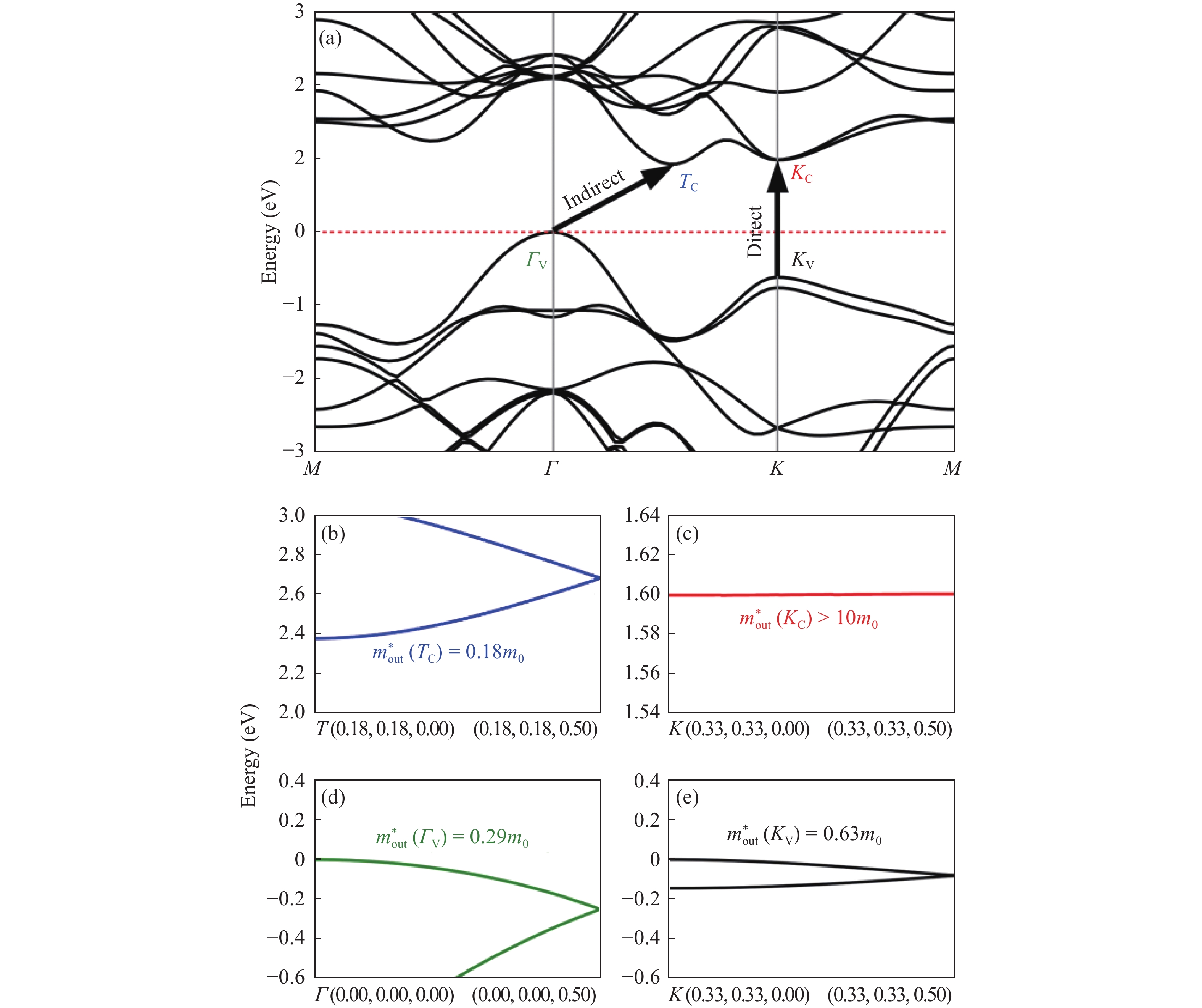
Fig. 2.  (Color online) (a) Calculated band structure of bulk MoS2, where the band-edge states forming the indirect and direct band-gap transitions are indicated. (b–e) The energy dispersion of the states marked in (a) along the out-of-layer direction for each band-edge state, based on which the out-of-layer components of effective mass ( $\scriptstyle{m_{\rm{out}}^*}$ ) are calculated.

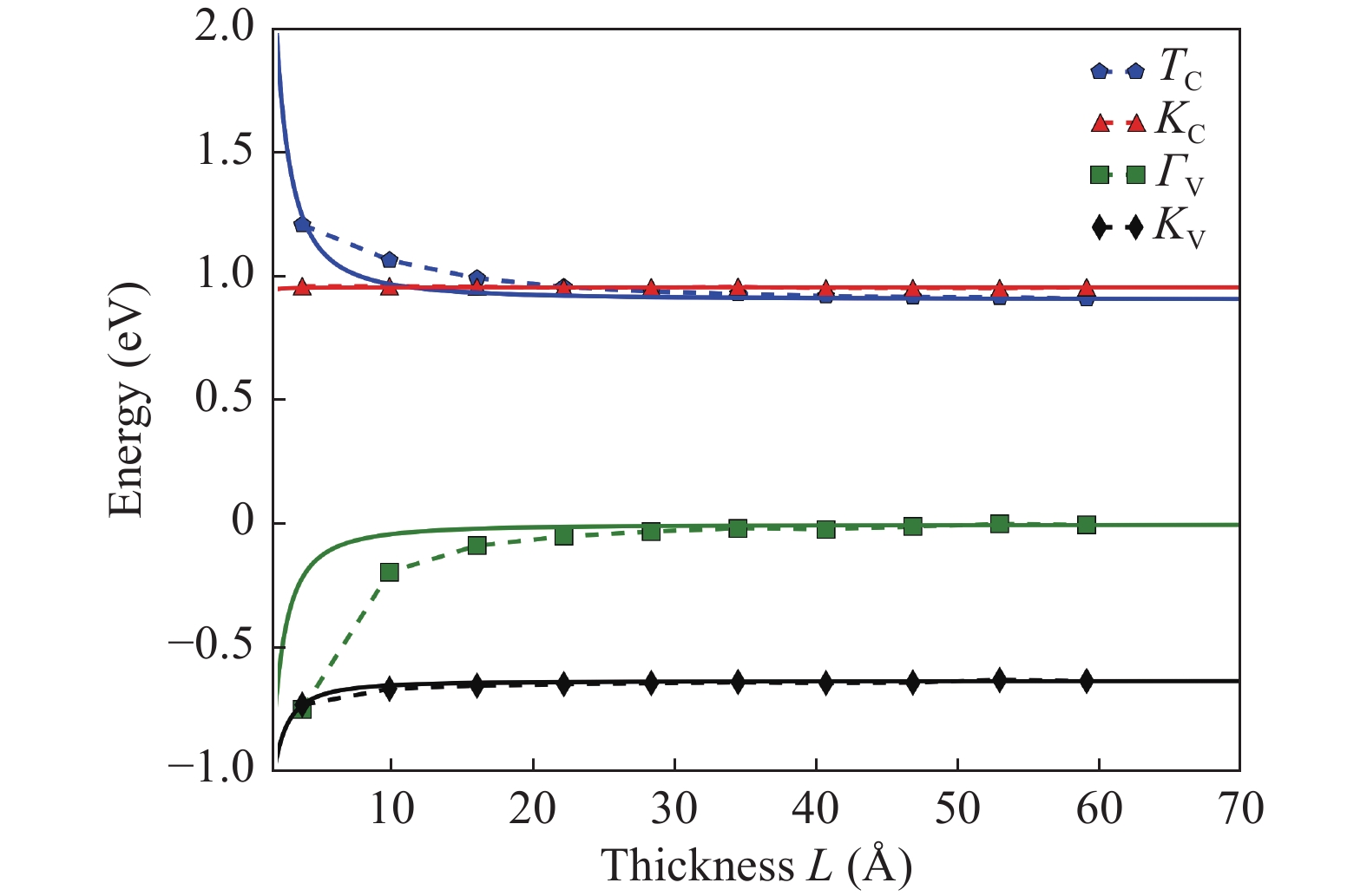
Fig. 3.  (Color online) Evolution of calculated band energies of the band-edge states determining the indirect to direct band-gap transition with the thickness L for MoS2. The solid lines represent the fitting results based on the finite potential-well model (i.e., the equation mentioned above with n = 1). The dash lines are drawn as a guide to the eye.

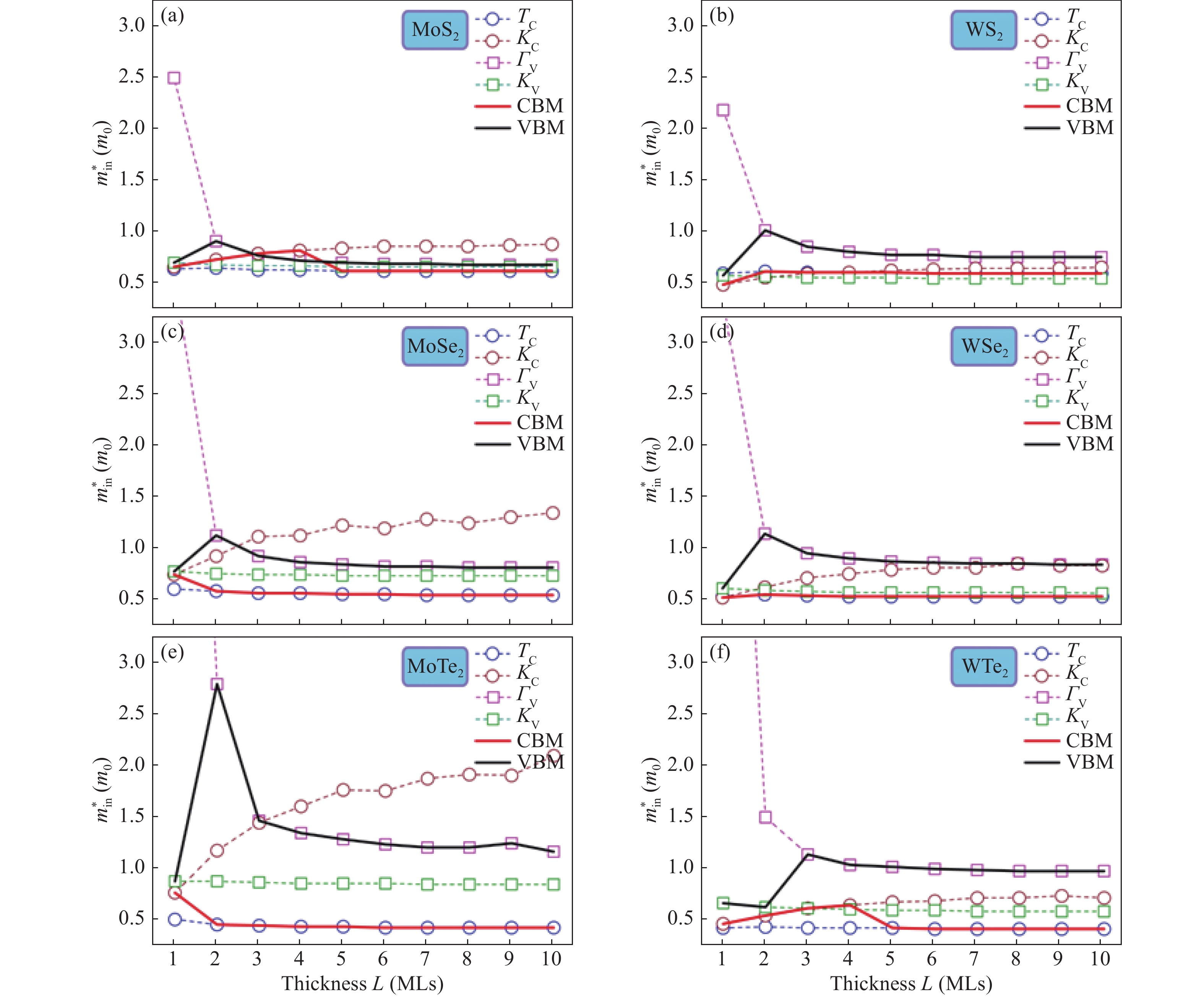
Fig. 5.  (Color online) Evolution of the in-layer component of effective mass ( $m_{\rm{in}}^*$ ) of the relevant band-edge states with the layer thickness L for all the investigated group-VIB TMDs MX2 (M = Mo, W and X = S, Se, Te). The actual CBM and VBM states are depicted by the solid black and red lines, respectively.

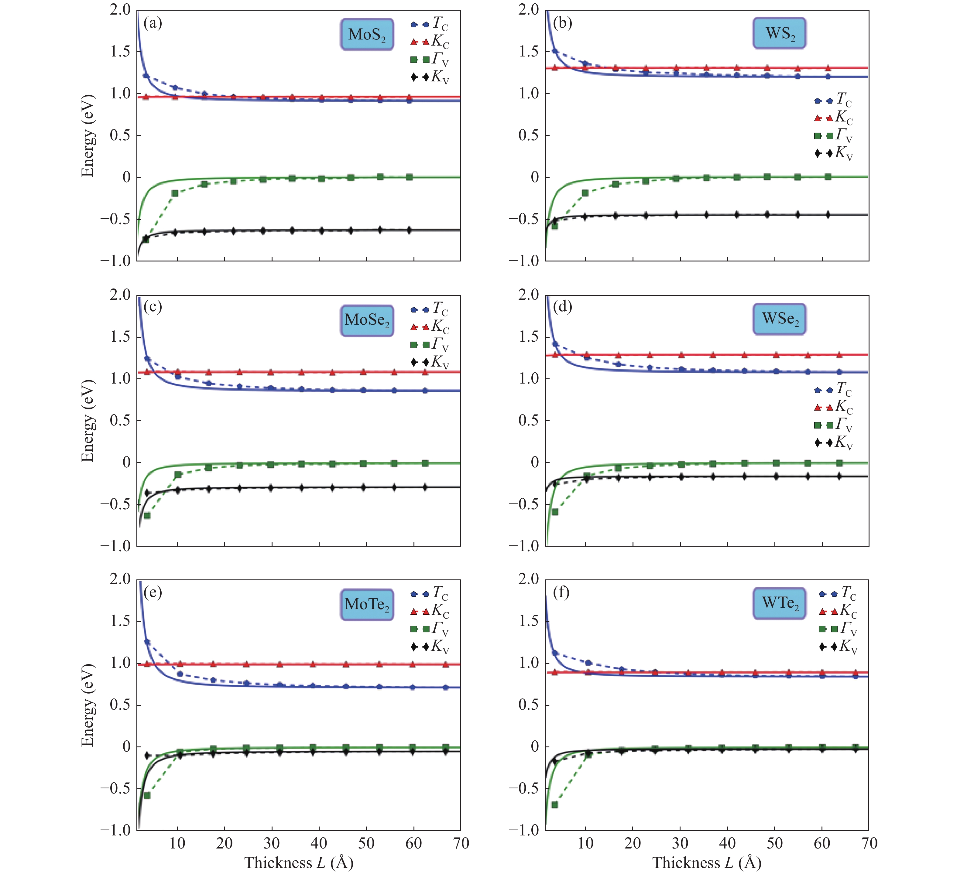
Fig. 4.  (Color online) Evolution of band energies of the relevant band-edge states with the thickness L for all the investigated group-VIB TMDs MX2 (M = Mo, W and X = S, Se, Te). Similar to Fig. 3, the solid lines represent the fitting results based on the finite potential-well model and the dash lines are drawn as a guide to the eye.

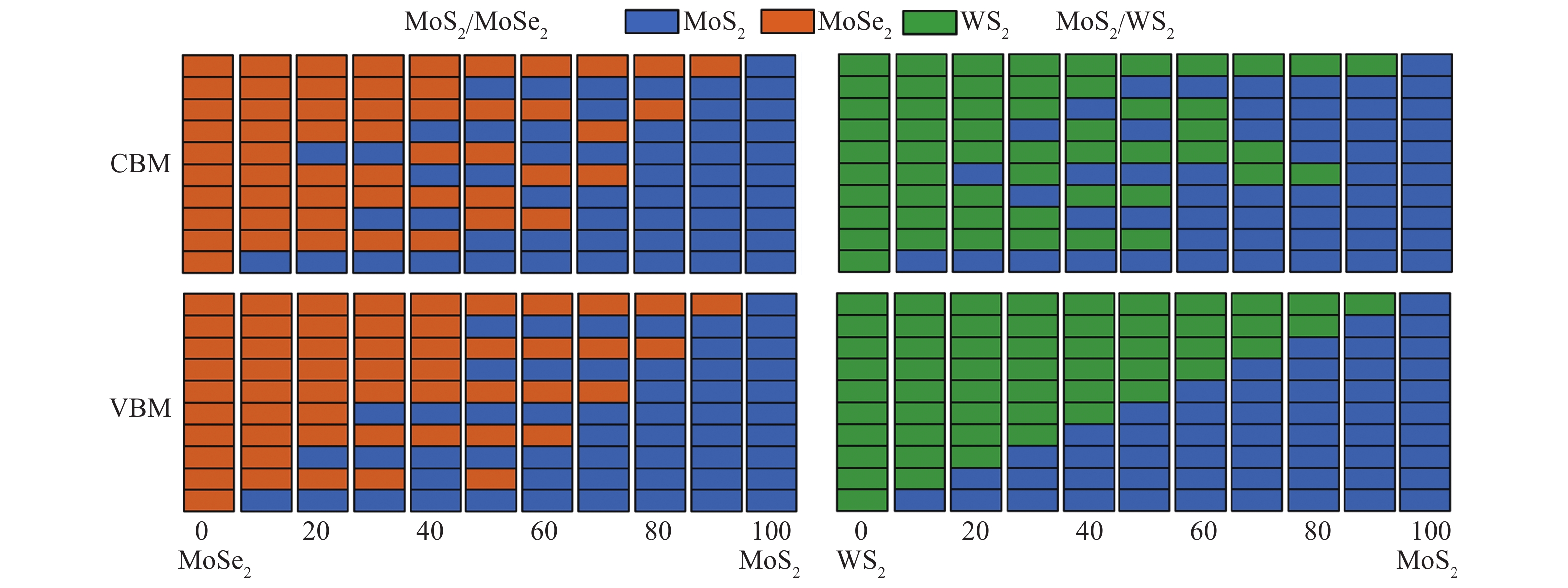
S1.  (Color online) the scheme of the stacking orders for each structures with the lowest $m_{\rm{in}}^*$ for CBMs and VBMs in MoS2/MoSe2 and MoS2/WS2 heterostructures.

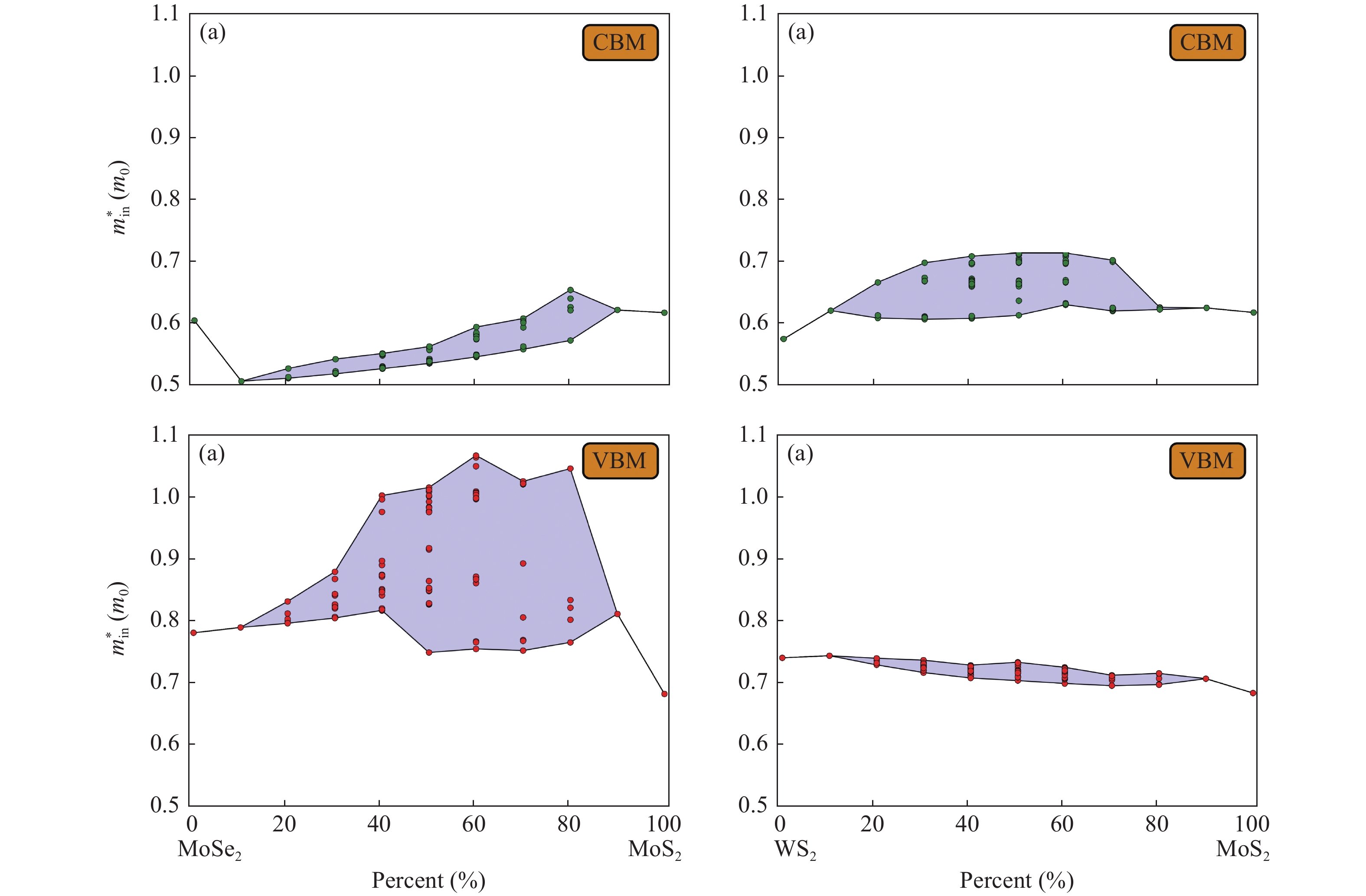
Fig. 6.  (Color online) Calculated in-layer component of effective mass ( $m_{\rm{in}}^*$ ) for the van der Waals heterostructures formed by two TMD materials (see the main text) as the function of the content of constituted TMD. Each data point represents the specific ordering of two TMDs arrangement along the out-of-layer direction at some compositon.

Table 1.   Calculated out-of-layer components of effective mass ( $m_{\rm{out}}^*$ ) of the relevant band-edge states of TC, KC, ΓV, and KV for the bulk phase of MX2 (M = Mo, W and X = S, Se, Te). The unit of $m_{\rm{out}}^*$ is m0.

Parameter $m_{{\rm{out}}}^*\left( {{T_{\rm{C}}}} \right)$ $m_{{\rm{out}}}^*\left( {{K_{\rm{C}}}} \right)$ $m_{{\rm{out}}}^*\left( {{\varGamma _{\rm{V}}}} \right)$ $m_{{\rm{out}}}^*\left( {{K_{\rm{V}}}} \right)$
MoS2 0.18 > 10.00 0.29 0.63
MoSe2 0.16 > 10.00 0.42 0.41
MoTe2 0.13 > 10.00 0.26 0.25
WS2 0.16 > 10.00 0.22 0.89
WSe2 0.30 > 10.00 0.33 1.98
WTe2 0.16 > 10.00 0.17 0.45
DownLoad: CSV

Table 2.   Calculated in-layer components of effective mass ( $m_{\rm{in}}^*$ ) of the relevant band-edge states of TC, KC, ΓV, and KV at the monolayer limit and the thick enough layers of 10 monolayers. All the synthesized TMD materials of MX2 (M = Mo, W and X = S, Se, Te) are calculated.

Parameter Layers $m_{{\rm{in}}}^*\left( {{T_{\rm{C}}}} \right)$ $m_{{\rm{in}}}^*\left( {{K_{\rm{C}}}} \right)$ $m_{{\rm{in}}}^*\left( {{\varGamma _{\rm{V}}}} \right)$ $m_{{\rm{in}}}^*\left( {{K_{\rm{V}}}} \right)$
MoS2 1 0.63 0.65 2.49 0.69
10 0.61 0.87 0.67 0.65
MoSe2 1 0.60 0.74 3.63 0.77
10 0.54 1.34 0.81 0.73
MoTe2 1 0.49 0.75 10.93 0.86
10 0.41 1.34 1.15 0.83
WS2 1 0.59 0.75 2.18 0.57
10 0.59 2.08 0.75 0.54
WSe2 1 0.54 0.48 3.43 0.62
10 0.54 0.65 0.85 0.57
WTe2 1 0.43 0.53 8.74 0.67
10 0.42 0.84 0.98 0.59
DownLoad: CSV
[1]
Novoselov K S, Geim A K, Morozov S V, et al. Electric field effect in atomically thin carbon films. Science, 2004, 306(5696): 666 doi: 10.1126/science.1102896
[2]
Allen M J, Tung V C, Kaner R B. Honeycomb carbon: a review of graphene. Chem Rev, 2010, 110(1): 132 doi: 10.1021/cr900070d
[3]
Novoselov K S, Jiang D, Schedin F, et al. Two-dimensional atomic crystals. Proc Natl Acad Sci USA, 2005, 102(30): 10451 doi: 10.1073/pnas.0502848102
[4]
Fivaz R, Mooser E. Mobility of charge carriers in semiconducting layer structures. Phys Rev, 1967, 163(3): 743 doi: 10.1103/PhysRev.163.743
[5]
Radisavljevic B, Radenovic A, Brivio J, et al. Single-layer MoS2 transistors. Nat Nano, 2011, 6(3): 147 doi: 10.1038/nnano.2010.279
[6]
Mak K F, Lee C G, Hone J, et al. Atomically thin MoS2: a new direct-gap semiconductor. Phys Rev Lett, 2010, 105(13): 136805 doi: 10.1103/PhysRevLett.105.136805
[7]
Tongay S, Zhou J, Ataca C, et al. Thermally driven crossover from indirect toward direct bandgap in 2D semiconductors: MoSe2 versus MoS2. Nano Lett, 2012, 12(11): 5576 doi: 10.1021/nl302584w
[8]
Jin W C, Yeh P C, Zaki N, et al. Direct measurement of the thickness-dependent electronic band structure of MoS2 using angle-resolved photoemission spectroscopy. Phys Rev Lett, 2013, 111(10): 106801 doi: 10.1103/PhysRevLett.111.106801
[9]
Zhang Y, Chang T R, Zhou B, et al. Direct observation of the transition from indirect to direct bandgap in atomically thin epitaxial MoSe2. Nat Nano, 2014, 9(2): 111 doi: 10.1038/nnano.2013.277
[10]
Kośmider K, Fernández-Rossier J. Electronic properties of the MoS2-WS2 heterojunction. Phys Rev B, 2013, 87(7): 075451 doi: 10.1103/PhysRevB.87.075451
[11]
Terrones H, López-Urías F, Terrones M. Novel hetero-layered materials with tunable direct band gaps by sandwiching different metal disulfides and diselenides. Sci Rep, 2013, 3: 1549 doi: 10.1038/srep01549
[12]
Geim A K, Grigorieva I V. Van der Waals heterostructures. Nature, 2013, 499(7459): 419 doi: 10.1038/nature12385
[13]
Komsa H P, Krasheninnikov A V. Electronic structures and optical properties of realistic transition metal dichalcogenide heterostructures from first principles. Phys Rev B, 2013, 88(8): 085318 doi: 10.1103/PhysRevB.88.085318
[14]
Conley H J, Wang B, Ziegler J I, et al. Bandgap engineering of strained monolayer and bilayer MoS2. Nano Lett, 2013, 13(8): 3626 doi: 10.1021/nl4014748
[15]
Zhu C R, Wang G, Liu B L, et al. Strain tuning of optical emission energy and polarization in monolayer and bilayer MoS2. Phys Rev B, 2013, 88(12): 121301 doi: 10.1103/PhysRevB.88.121301
[16]
Feng J, Qian X F, Huang C W, et al. Strain-engineered artificial atom as a broad-spectrum solar energy funnel. Nat Photon, 2012, 6(12): 866 doi: 10.1038/nphoton.2012.285
[17]
Johari P, Shenoy Vivek B. Tuning the electronic properties of semiconducting transition metal dichalcogenides by applying mechanical strains. ACS Nano, 2012, 6(6): 5449 doi: 10.1021/nn301320r
[18]
He K L, Poole C, Mak K F, et al. Experimental demonstration of continuous electronic structure tuning via strain in atomically thin MoS2. Nano Lett, 2013, 13(6): 2931 doi: 10.1021/nl4013166
[19]
Peelaers H, Van de Walle C G. Effects of strain on band structure and effective masses in MoS2. Phys Rev B, 2012, 86(24): 241401 doi: 10.1103/PhysRevB.86.241401
[20]
Qi J S, Li X, Qian X F, et al. Bandgap engineering of rippled MoS2 monolayer under external electric field. Appl Phys Lett, 2013, 102(17): 173112 doi: 10.1063/1.4803803
[21]
Wu S F, Ross J S, Liu, G B, et al. Electrical tuning of valley magnetic moment through symmetry control in bilayer MoS2. Nat Phys, 2013, 9(3): 149 doi: 10.1038/nphys2524
[22]
Chang J, Larentis S, Tutuc E, et al. Atomistic simulation of the electronic states of adatoms in monolayer MoS2. Appl Phys Lett, 2014, 104(14): 141603 doi: 10.1063/1.4870767
[23]
Sengupta A, Mahapatra S. Performance limits of transition metal dichalcogenide (MX2) nanotube surround gate ballistic field effect transistors. J Appl Phys, 2013, 113(19): 194502 doi: 10.1063/1.4805059
[24]
Sengupta A, Chanana A, Mahapatra S. Phonon scattering limited performance of monolayer MoS2 and WSe2 n-MOSFET. AIP Adv, 2015, 5(2): 027101 doi: 10.1063/1.4907697
[25]
Wang Q H, Kalantar-Zadeh K, Kis A, et al. Electronics and optoelectronics of two-dimensional transition metal dichalcogenides. Nat Nano, 2012, 7(11): 699 doi: 10.1038/nnano.2012.193
[26]
Chhowalla M, Shin H S, Eda G, et al. The chemistry of two-dimensional layered transition metal dichalcogenide nanosheets. Nat Chem, 2013, 5(4): 263 doi: 10.1038/nchem.1589
[27]
Eda G, Maier S A. Two-dimensional crystals: managing light for optoelectronics. ACS Nano, 2013, 7(7): 5660 doi: 10.1021/nn403159y
[28]
Lebègue S, Eriksson O. Electronic structure of two-dimensional crystals from ab initio theory. Phys Rev B, 2009, 79(11): 115409 doi: 10.1103/PhysRevB.79.115409
[29]
Han S W, Kwon H, Kim S K, et al. Band-gap transition induced by interlayer van der Waals interaction in MoS2. Phys Rev B, 2011, 84(4): 045409 doi: 10.1103/PhysRevB.84.045409
[30]
Jo S, Costanzo D, Berger H, et al. Electrostatically induced superconductivity at the surface of WS2. Nano Lett, 2015, 15(2): 1197 doi: 10.1021/nl504314c
[31]
Kang J, Zhang L J, Wei S H. A unified understanding of the thickness-dependent bandgap transition in hexagonal two-dimensional semiconductors. J Phys Chemry Lett, 2016, 7(4): 597 doi: 10.1021/acs.jpclett.5b02687
[32]
Kresse G, Hafner J. Ab initio molecular dynamics for liquid metals. Phys Rev B, 1993, 47(1): 558 doi: 10.1103/PhysRevB.47.558
[33]
Kresse G, Hafner J. Ab initio molecular-dynamics simulation of the liquid-metal-amorphous-semiconductor transition in germanium. Phys Rev B, 1994, 49(20): 14251 doi: 10.1103/PhysRevB.49.14251
[34]
Kresse G, Furthmüller J. Efficiency of ab-initio total energy calculations for metals and semiconductors using a plane-wave basis set. Comput Mater Sci, 1996, 6(1): 15 doi: 10.1016/0927-0256(96)00008-0
[35]
Kresse G, Furthmüller J. Efficient iterative schemes for ab initio total-energy calculations using a plane-wave basis set. Phys Rev B, 1996, 54(16): 11169 doi: 10.1103/PhysRevB.54.11169
[36]
Blöchl P E. Projector augmented-wave method. Phys Rev B, 1994, 50(24): 17953 doi: 10.1103/PhysRevB.50.17953
[37]
Kresse G, Joubert D. From ultrasoft pseudopotentials to the projector augmented-wave method. Phys Rev B, 1999, 59(3): 1758 doi: 10.1103/PhysRevB.59.1758
[38]
Perdew J P, Burke K, Ernzerhof M. Generalized gradient approximation made simple. Phys Rev Lett, 1996, 77(18): 3865 doi: 10.1103/PhysRevLett.77.3865
[39]
Grimme S. Semiempirical GGA-type density functional constructed with a long-range dispersion correction. J Comput Chem, 2006, 27(15): 1787 doi: 10.1002/(ISSN)1096-987X
[40]
Yun W S, Han S W, Hong S C, et al. Thickness and strain effects on electronic structures of transition metal dichalcogenides: 2H-MX2 semiconductors (M = Mo, W; X = S, Se, Te). Phys Rev B, 2012, 85(3): 033305 doi: 10.1103/PhysRevB.85.033305
[41]
Rao K S, Senthilnathan J, Liu Y F, et al. Role of peroxide ions in formation of graphene nanosheets by electrochemical exfoliation of graphite. Sci Rep, 2014, 4: 4237 doi: 10.1038/srep04237
[42]
Li X D. Intrinsic electrical transport properties of monolayer silicene and MoS2 from first principles. Phys Rev B, 2013, 87: 115418 doi: 10.1103/PhysRevB.87.115418
[43]
Ataca C, Şahin H, Ciraci S. Stable, dingle-layer MX2 transition-metal oxides and dichalcogenides in a honeycomb-like structure. J Phys Chem C, 2012, 116(16): 8983 doi: 10.1021/jp212558p
[44]
Zhang L J, Zunger A. Evolution of electronic structure as a function of layer thickness in group-VIB transition metal dichalcogenides: emergence of localization prototypes. Nano Lett, 2015, 15(2): 949 doi: 10.1021/nl503717p
[45]
Kumar A, Ahluwalia P K. Electronic structure of transition metal dichalcogenides monolayers 1H-MX2 (M = Mo, W; X = S, Se, Te) from ab-initio theory: new direct band gap semiconductors. Eur Phys J B, 2012, 85(6): 186 doi: 10.1140/epjb/e2012-30070-x
[46]
Böker T, Severin R, Müller A, et al. Band structure of MoS2, MoSe2, and α-MoTe2: Angle-resolved photoelectron spectroscopy and ab initio calculations. Phys Rev B, 2001, 64(23): 235305 doi: 10.1103/PhysRevB.64.235305

17100018supp.pdf

  • Search

    Advanced Search >>

    GET CITATION

    shu

    Export: BibTex EndNote

    Article Metrics

    Article views: 6042 Times PDF downloads: 147 Times Cited by: 0 Times

    History

    Received: 24 October 2017 Revised: Online: Uncorrected proof: 19 April 2018Accepted Manuscript: 26 April 2018Published: 01 July 2018

    Catalog

      Email This Article

      User name:
      Email:*请输入正确邮箱
      Code:*验证码错误
      Yuanhui Sun, Xinjiang Wang, Xin-Gang Zhao, Zhiming Shi, Lijun Zhang. First-principle high-throughput calculations of carrier effective masses of two-dimensional transition metal dichalcogenides[J]. Journal of Semiconductors, 2018, 39(7): 072001. doi: 10.1088/1674-4926/39/7/072001 ****Y H Sun, X J Wang, X G Zhao, Z M Shi, L J Zhang, First-principle high-throughput calculations of carrier effective masses of two-dimensional transition metal dichalcogenides[J]. J. Semicond., 2018, 39(7): 072001. doi: 10.1088/1674-4926/39/7/072001.
      Citation:
      Yuanhui Sun, Xinjiang Wang, Xin-Gang Zhao, Zhiming Shi, Lijun Zhang. First-principle high-throughput calculations of carrier effective masses of two-dimensional transition metal dichalcogenides[J]. Journal of Semiconductors, 2018, 39(7): 072001. doi: 10.1088/1674-4926/39/7/072001 ****
      Y H Sun, X J Wang, X G Zhao, Z M Shi, L J Zhang, First-principle high-throughput calculations of carrier effective masses of two-dimensional transition metal dichalcogenides[J]. J. Semicond., 2018, 39(7): 072001. doi: 10.1088/1674-4926/39/7/072001.

      First-principle high-throughput calculations of carrier effective masses of two-dimensional transition metal dichalcogenides

      doi: 10.1088/1674-4926/39/7/072001
      Funds:

      Project supported by the National Natural Science Foundation of China (Nos. 11404131, 11674121), the Program for JLU Science and Technology Innovative Research Team, and the Special Fund for Talent Exploitation in Jilin Province of China.

      More Information

      Catalog

        /

        DownLoad:  Full-Size Img  PowerPoint
        Return
        Return