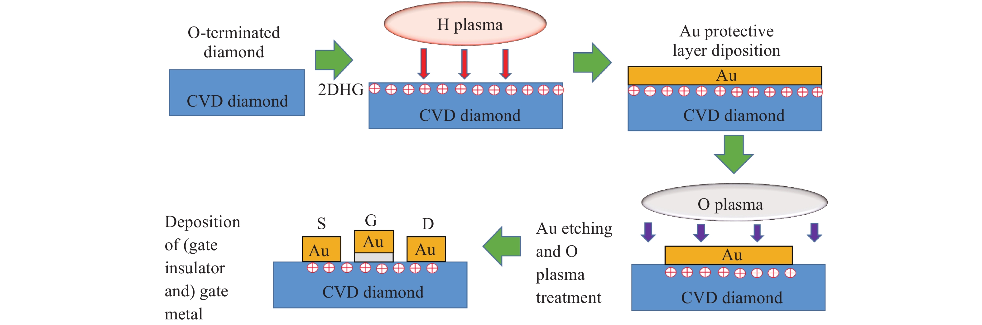
J. Semicond. > 2018, Volume 39 > Issue 7 > 074003

SEMICONDUCTOR DEVICES

Research on the hydrogen terminated single crystal diamond MOSFET with MoO3 dielectric and gold gate metal

Zeyang Ren, Jinfeng Zhang, Jincheng Zhang, Chunfu Zhang, Pengzhi Yang, Dazheng Chen, Yao Li and Yue Hao

+ Author Affiliations

 Corresponding author: Jinfeng Zhang, Email: jfzhang@xidian.edu.cn; Jincheng Zhang, jchzhang@xidian.edu.cn

DOI: 10.1088/1674-4926/39/7/074003

PDF

Turn off MathJax

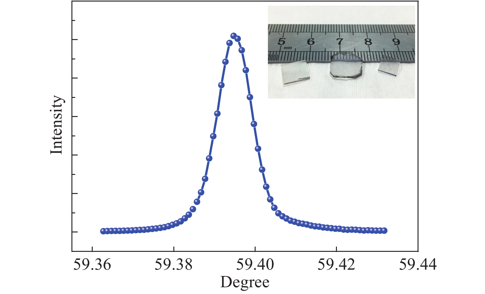
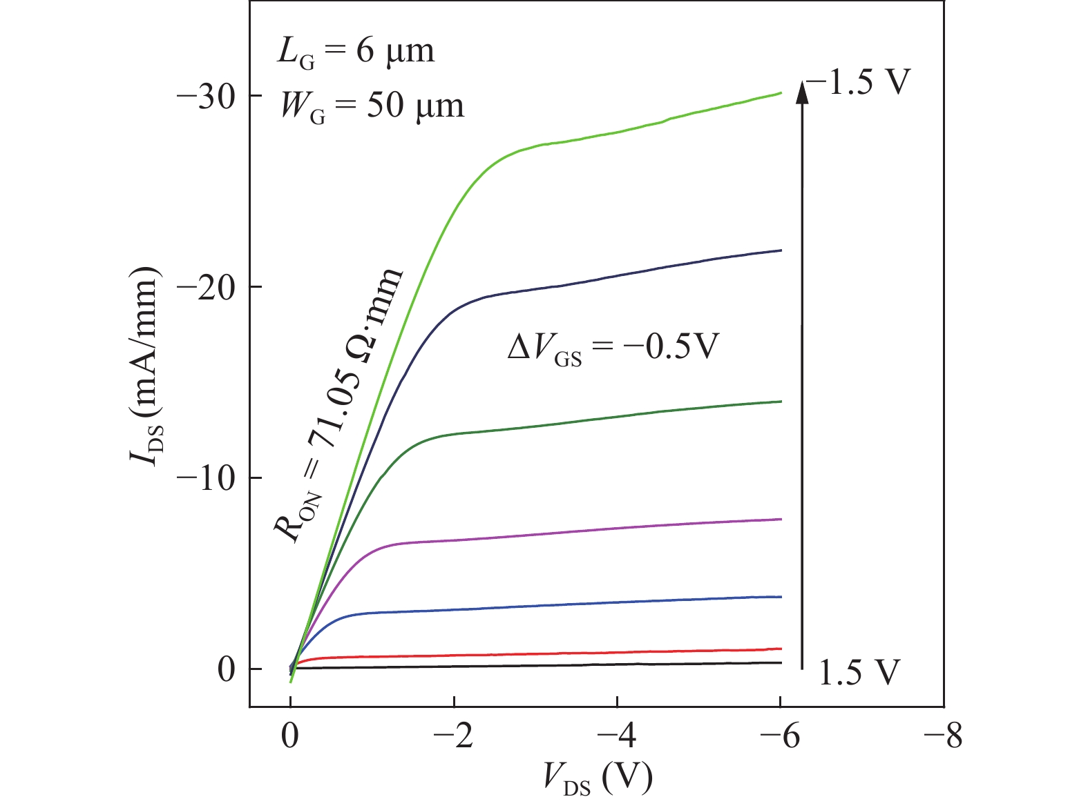
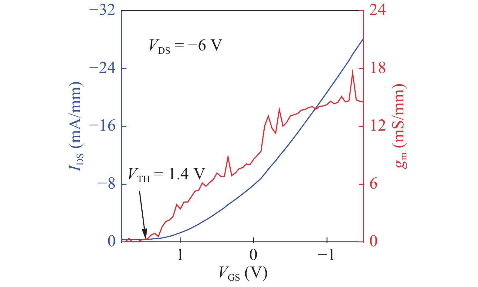
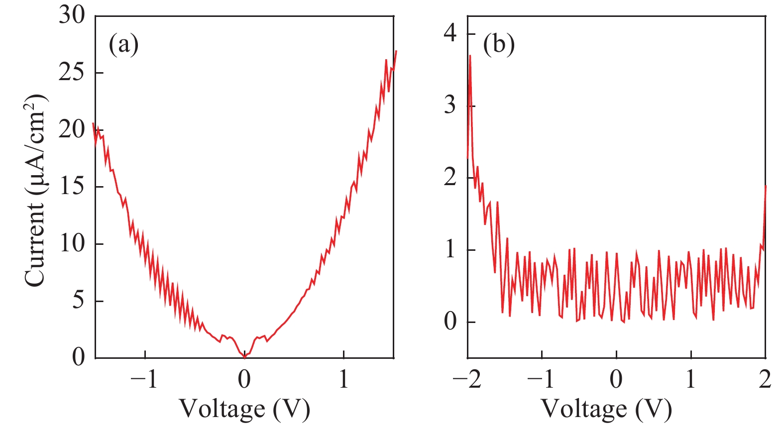
Abstract: The single crystal diamond with maximum width about 10 mm has been grown by using microwave plasma chemical vapor deposition equipment. The quality of the grown diamond was characterized using an X-ray diffractometer. The FWHM of the (004) rocking curve is 37.91 arcsec, which is comparable to the result of the electronic grade single crystal diamond commercially obtained from Element Six Ltd. The hydrogen terminated diamond field effect transistors with Au/MoO3 gates were fabricated based on our CVD diamond and the characteristics of the device were compared with the prototype Al/MoO3 gate. The device with the Au/MoO3 gate shows lower on-resistance and higher gate leakage current. The detailed analysis indicates the presence of aluminum oxide at the Al/MoO3 interface, which has been directly demonstrated by characterizing the interface between Al and MoO3 by X-ray photoelectron spectroscopy. In addition, there should be a surface transfer doping effect of the MoO3 layer on H-diamond even with the atmospheric-adsorbate induced 2DHG preserved after MoO3 deposition.

Key words: single crystal diamondMOSFETMoO3transfer doping

Diamond has been considered as the ultimate semiconductor material due to its outstanding properties[1]. However, the lack of large area substrate and suitable dopants has severely obstructed the wide application of the single crystal diamond (SCD)[24]. The two dimensional hole gas (2DHG) at a hydrogen terminated diamond (H-diamond) surface induced by atmospheric adsorbates[5] or solid-state acceptor transfer doping[68] has been widely used to develop diamond electronic devices. Currently, the H-diamond field effect transistors (FETs) have achieved the cut-off frequency (fT) of 53 GHz[9] and the maximum oscillation frequency (fMAX) of 120 GHz[10], and the high breakdown voltage of more than 1 kV has also been realized[11]. As one of the transfer doping dielectrics[12], a 10-nm-thick MoO3 layer deposited on H-diamond surface could induce a 2DHG with a sheet hole density as high as 1014 cm−2[13]. We have reported the SCD MOSFET with the MoO3 gate dielectric deposited on an H-diamond surface preserving atmospheric-adsorbate-induced 2DHG very recently[14]. The device shows a low on-resistance (RON) and a high transconductance compared with the diamond MOSFETs with other dielectrics such as HfO2[15], and ZrO2[16]. However, the transfer doping effect is not evidently shown. What is more, the extracted permittivity of MoO3 is quite low compared with the previously reported data[17]. We have suggested there may be aluminum oxide at the interface between MoO3 and the aluminum gate metal.

In this paper, we report the device characteristics of the SCD MOSFET with MoO3 gate dielectric and gold gate metal, and make a comparison with our Al/MoO3-gated device to investigate the characteristics of MoO3 and verify the existence of aluminum oxide at the Al/MoO3 interface.

The SCD was grown on a HPHT (100) seed in a microwave plasma chemical vapor deposition (MPCVD) chamber with only methane and hydrogen introduced in the growth. In order to achieve the stable thermal exchange between the diamond sample and the water chiller during growth, the seed was brazed on a molybdenum holder using a 25-μm-thick gold layer. Before growth the seed was etched in the hydrogen plasma atmosphere with the addition of 2% oxygen for one hour. The purity of the hydrogen and methane used in this experiment was 6N and 5N5, respectively. During growth the pressure was maintained in 320 mbar, while the growth temperature and microwave power were in the range of 900–925 °C and 3.8 kW, respectively. The total gas flow rate and methane concentration were 200 sccm and 6%, respectively. After growth, the as-grown SCD was cut from the seed by laser and polished to achieve the surface root mean square (RMS) roughness below 1 nm. The quality of the CVD grown SCD was characterized by an X-ray diffractometer (XRD).

Based on the grown SCD plates, we have fabricated the H-diamond MOSFETs. Fig. 1 shows a schematic diagram of the device fabrication processes. Firstly, the substrate was immersed in the H2SO4/HNO3 (1 : 1) mixture at 250 °C for one hour to remove the non-diamond phase and obtain the oxygen terminated diamond (O-diamond) surface. Then the samples were kept in hydrogen plasma for 10 min at 900 °C to generate a hydrogen-terminated surface, and then cooled down to room temperature in a H2 gas flow. Before any device fabrication process, we measured the sheet resistivity, carrier concentration and carrier mobility of the H-terminated diamond substrate by using HL5500 equipment. Two substrates for Al and Au gated devices show similar electrical properties. The substrate for the FETs with Au gate metal shows the carrier mobility, carrier concentration and sheet resistivity of 106 cm2/(V·s), 5.90 × 1012 cm−2 and 9.91 kΩ, respectively. The substrate for the FETs with Al gate metal shows the carrier mobility, carrier concentration and sheet resistivity of 103 cm2/(V·s), 5.67 × 1012 cm−2 and 10.68 kΩ, respectively. After this, a 100-nm-thick layer of gold was deposited on the H-diamond surface by thermal evaporation to prevent the surface from contacting the photoresist during the device process[18]. At the same time, the gold layer provides an ohmic contact due to the unpinned nature of the H-terminated diamond surface and the proper work function of the gold[19]. After active-region lithography and wet etching of gold in a KI/I2 solution, the diamond surfaces around the outside edges of the devices were exposed to low power oxygen plasma treatment to form the isolation regions due to pinning the Fermi-level of the O-terminated surface at approximately 1.7 eV above the valence band edge[20]. After the gate window lithography followed by Au selective wet etching, source and drain contacts of the devices are formed, and the lateral etching of gold below the photoresist gives rise to the gap between the source (or drain) and the gate metal yet to be deposited. Then the 40-nm-thick MoO3 and 100-nm-thick layer of gold deposition and lift-off were performed to form the gates of the devices. Finally, the H-diamond MOSFET with the gate length of 6 μm was achieved. The direct current characteristics were measured at room temperature by using a Keithley 4200 semiconductor parameter analyzer.

Figure  1.  (Color online) Schematic diagram of the device fabrication processes.

The picture of the CVD grown SCD after cutting from seed and polishing carefully is shown in the inset of Fig. 2. The single crystal diamond with the maximum width about 10 mm has been achieved, which is the biggest one among reported results as far as we know. The full width at half maximum of the (004) rocking curve is measured to be 37.91 arcsec (Fig. 2), which is comparable to the result of the electronic grade single crystal diamond (34.98 arcsec) commercially obtained from Element Six Ltd. After hydrogen plasma treatment, the surface of the sample was characterized by an atomic force microscope (AFM). The result is shown in Fig. 3. The RMS roughness of the post H-diamond surface is 0.522 nm. We also obtained the AFM morphology of the MoO3 layer with the thickness of 10 and 40 nm. The results are shown in Fig. 4. The 10-nm-thick MoO3 shows the RMS roughness of 0.302 nm, and some pit depths to 3.9 nm exist in the layer. The 40-nm-thick MoO3 layer shows the RMS roughness of 0.240 nm.

Figure  2.  (Color online) XRD result of (004) rocking curve of the CVD grown SCD.
Figure  3.  (Color online) Surface morphology of the SCD after hydrogen plasma treatment.
Figure  4.  Surface morphology of the (a) 10 nm and (b) 40 nm MoO3 layer.

The output characteristics of the transistor with a gate length of 6 μm (Fig. 5) demonstrate a saturation drain current (IDsat) of −30 mA/mm and an on-resistance (RON) of 71.05 Ω·mm at the VGS of −1.5 V. Compared with our diamond MOSFET with 4-μm Al/MoO3 gate[14], the IDsat value is at the same level, and the RON value is even lower. Note that drain current appears at the VDS = 0 V, and it indicates the presence of gate leakage current.

Figure  5.  (Color online) Output characteristics of the H-diamond MOSFET.

We measured the gate current–voltage (IGVG) characteristics of the gate–drain diode (Fig. 6). A relatively high gate leakage current is demonstrated for both forward and reverse bias, and the current is about four orders of magnitude higher than the Al/MoO3-gated transistor, though the MoO3 layer used in this report has a four times thickness (40 nm). We have conjectured that maybe the MoO3 dielectric was fairly leaky. To test the MoO3 dielectric further, on a corner of this diamond sample we have deposited a 40-nm-thick MoO3 layer on the FETs with all the device processes mentioned in part 2 finished, and measured the leakage current across the device isolation region with the MoO3 layer on an O-diamond surface. The distance between the gold electrodes, the drain for a FET and the source for a neighboring FET, was 20 μm. The measured current is below 10−7 A at the voltage of 5 V, and it is at the same level with the leakage of the device isolation region with no MoO3 layer deposited, so the MoO3 layer on the O-diamond surface does not bring observable extra leakage.

Figure  6.  (Color online) Gate current–voltage characteristics of the MoO3/H-diamond MOS structure.

Based on all these phenomena observed on H-diamond MOSFET with MoO3 gate dielectric and gold or aluminum gate metal, we suggest that the MoO3 dielectric on O-diamond surface shows a much better insulating property than the prototype on H-diamond. This difference indicates there should be a surface transfer doping effect of the MoO3 layer on H-diamond even when the atmospheric-adsorbate induced 2DHG was preserved after MoO3 deposition in our cases. The effect leads to electrons transferring to the MoO3 layer from H-diamond surface, and so the conductivity of the MoO3 layer increases. Then the much lower leakage of Al/MoO3/H-diamond MOS structure than that of the Au/MoO3/H-diamond structure could be attributed mainly to the appearance of unintentionally introduced aluminum oxide as an insulating layer at the interface between aluminum and the MoO3 layer.

The lower RON of the Au/MoO3-gated diamond MOSFET may indicate higher hole density in the channel because the sheet hole density for the MoO3 transfer doped H-diamond will increase with the increasing thickness of the MoO3 layer[13]. Meanwhile, the transfer characteristic of the transistor shows the maximum transconductance (gmmax) of 15 mS/mm, and the threshold voltage (VTH) of 1.4 V (Fig. 7). That is to say, only about 50 % gmmax reduction occurred for our MoO3-gated MOSFET with the gold gate compared with the one with the aluminum gate at the same gate voltage (gmmax = 29 mS/mm at VGS = −1.5 V)[14]. Based on the changes of gate length, MoO3 layer thickness and VTH and the same device process, this also supports that the hole density in the channel increases in the Au/MoO3-gated diamond MOSFET.

Figure  7.  (Color online) Transfer characteristics of the H-diamond MOSFET.

In order to make a contrastive study of the interface between Al/MoO3 and Au/MoO3, we fabricated the Au/MoO3/Au and Al/MoO3/Au structure with the same thickness of metal and oxide. Then, we measured the IV characteristics of the structure. The results are shown in Fig. 8. The Au/MoO3/Au structure shows an almost symmetrical IV curve (Fig. 8(a)), and the current is higher than the Al/MoO3/Au structure (Fig. 8(b)). In addition, the shape of the IV curve of the Au/MoO3/Au structure is almost the same with the gate current of our FET. However, the value of the current is lower than the gate leakage current. There is no transfer doping effect existing in the metal–MoO3–metal structure. Thus, the current of the metal–MoO3–metal structure is very low.

Figure  8.  (Color online) The IV curve of (a) Au/MoO3/Au and (b) Al/MoO3/Au structure.

Based on the above analyses, we can conclude that aluminum oxide exists in the interface between the Al and MoO3, which contributes to the low gate leakage current of the Al gate devices. In order to obtain the direct evidences for the generation of aluminum oxide between Al/MoO3 layers, we deposited the Al (20 nm)/MoO3 (40 nm) on the insulated substrate. Then we measured the Al surface, the inner of the Al metal and the interface between Al and MoO3 by using X-ray photoelectron spectroscopy. We etched the Al metal using argon plasma in order to obtain the inner of Al and the interface between Al/MoO3 layers. The results of the XPS spectrum are shown in Fig. 9. The spectra obtained at the interface is similar to the result obtained at the Al surface and is different with the inner of the Al. Fig. 10 shows the spectrum of Al peaks. We can see clearly the difference of the peaks. At the surface and the interface, there is higher peak intensity at a high binding energy. At the surface of Al, the Al is exposed to the air atmosphere. Thus, the Al at the surface will be oxidized to aluminum oxide. The result in the interface is similar to the surface, which indicates the presence of aluminum oxide at the interface. The aluminum oxide at the interface is originally from the reaction of Al and the oxygen in MoO3.

Figure  9.  (Color online) XPS results of the Al metal surface, inner of the Al metal and the interface between Al and MoO3.
Figure  10.  (Color online) Spectrum of the Al related peaks of (a) the Al metal surface, (b) the inner of the Al metal, and (c) the interface between Al and MoO3.

The SCD with the maximum width about 10 mm has been grown by MPCVD and the quality of the CVD grown SCD is relatively high. Based on the CVD grown SCD, the H-diamond MOSFET with Au/MoO3 gates were fabricated. The device with a 6-μm Au/MoO3 gate shows lower on-resistance, quite high current, transconductance and high gate leakage current compared with the prototype with a 4-μm Al/MoO3 gate already reported by our group. We have directly demonstrated the existence of aluminum oxide in the interface between Al and MoO3 by X-ray photoelectron spectroscopy measurement, and there should be a surface transfer doping effect of the MoO3 layer on H-diamond even though the atmospheric-adsorbate induced 2DHG was preserved after MoO3 deposition.


[1]
Liu J, Ohata H, Liao M, et al. Logic circuits with hydrogenated diamond field-effect transistors. IEEE Electron Device Lett, 2017, 38(7): 922 doi: 10.1109/LED.2017.2702744
[2]
Yamada H, Chaykhana A, Umezawa H, et al. Fabrication and fundamental characterizations of tiled clones of single-crystal diamond with 1-inch size. Diamond Relat Mater, 2012, 24: 29 doi: 10.1016/j.diamond.2011.09.007
[3]
Yamasaki S, Gheeraert E, Koide Y. Doping and interface of homoepitaxial diamond for electronic applications. Mrs Bulletin, 2014, 39(6): 499 doi: 10.1557/mrs.2014.100
[4]
Yamada H, Chayahara A, Mokuno Y, et al. A 2-in. mosaic wafer made of a single-crystal diamond. Appl Phys Lett, 2014, 104(10): 201 doi: 10.1063/1.4868720
[5]
Landstrass M I, Ravi K V. Resistivity of chemical vapor deposited diamond films. Appl Phys Lett, 1989, 55(10): 975 doi: 10.1063/1.101694
[6]
Russell S A O, Cao L, Qi D, et al. Surface transfer doping of diamond by MoO3: A combined spectroscopic and Hall measurement study. Appl Phys Lett, 2013, 103(20): 22
[7]
Crawford K G, Cao L, Qi D, et al. Enhanced surface transfer doping of diamond by V2O5 with improved thermal stability. Appl Phys Lett, 2016, 108(4): 22
[8]
He B, Ng T W, Lo M F, et al. Surface transfer doping of cubic boron nitride films by MoO3 and tetrafluoro-tetracyanoquinodimethane (F4-TCNQ). Acs Appl Mater Interfaces, 2015, 7(18): 9851 doi: 10.1021/acsami.5b01779
[9]
Russell S A O, Sharabi S, Tallaire A, et al. Hydrogen-terminated diamond field-effect transistors with cutoff frequency of 53 GHz. IEEE Electron Device Lett, 2012, 33(10): 1471 doi: 10.1109/LED.2012.2210020
[10]
Ueda K, Kasu M, Yamauchi Y, et al. Diamond FET using high-quality polycrystalline diamond with fT of 45 GHz and fmax of 120 GHz. IEEE Electron Device Lett, 2006, 27(7): 570 doi: 10.1109/LED.2006.876325
[11]
Syamsul M, Kitabayashi Y, Takuya K, et al. High voltage stress induced in transparent polycrystalline diamond field-effect transistor and enhanced endurance using thick Al2O3 passivation layer. IEEE Electron Device Lett, 2017, 38(5): 607 doi: 10.1109/LED.2017.2685081
[12]
Russell S A O, Cao L, Qi D, et al. Surface transfer doping of diamond by MoO3: A combined spectroscopic and Hall measurement study. Appl Phys Lett, 2013, 103(20): 202112 doi: 10.1063/1.4832455
[13]
Tordjman M, Saguy C, Bolker A, et al. Superior surface transfer doping of diamond with MoO3. Adv Mater Interfaces, 2014, 1(3): 1300155 doi: 10.1002/admi.201300155
[14]
Ren Z, Zhang J, Zhang J, et al. Diamond field effect transistors with MoO3 gate dielectric. IEEE Electron Device Lett, 2017, 38(6): 786 doi: 10.1109/LED.2017.2695495
[15]
Liu J W, Liao M Y, Imura M, et al. Normally-off HfO2-gated diamond field effect transistors. Appl Phys Lett, 2013, 103(9): 1899
[16]
Liu J, Liao M, Imura M, et al. Low on-resistance diamond field effect transistor with high-k ZrO2 as dielectric. Sci Rep, 2014, 4(7416): 6395
[17]
Madelung O, Rössler U, Schulz M. MoO3: optical properties, dielectric constants. Landolt-Börnstein - Group III Condensed Matter, 2000, 41d: 1
[18]
Wang J J, He Z Z, Yu C, et al. Rapid deposition of polycrystalline diamond film by DC arc plasma jet technique and its RF MESFETs. Diamond Relat Mater, 2014, 43(2): 43
[19]
Calvani P, Girolami M, Trucchi D M, et al. DC and RF performance of surface channel MESFETs on H-terminated polycrystalline diamond. Diamond Relat Mater, 2009, 18(5): 786
[20]
Kasu M, Kobayashi N. High mobility and high crystalline-quality chemical-vapor-deposition grown homoepitaxial diamond. Diamond Relat Mater, 2003, 12(3): 413
Fig. 1.  (Color online) Schematic diagram of the device fabrication processes.

Fig. 2.  (Color online) XRD result of (004) rocking curve of the CVD grown SCD.

Fig. 3.  (Color online) Surface morphology of the SCD after hydrogen plasma treatment.

Fig. 4.  Surface morphology of the (a) 10 nm and (b) 40 nm MoO3 layer.

Fig. 5.  (Color online) Output characteristics of the H-diamond MOSFET.

Fig. 6.  (Color online) Gate current–voltage characteristics of the MoO3/H-diamond MOS structure.

Fig. 7.  (Color online) Transfer characteristics of the H-diamond MOSFET.

Fig. 8.  (Color online) The IV curve of (a) Au/MoO3/Au and (b) Al/MoO3/Au structure.

Fig. 9.  (Color online) XPS results of the Al metal surface, inner of the Al metal and the interface between Al and MoO3.

Fig. 10.  (Color online) Spectrum of the Al related peaks of (a) the Al metal surface, (b) the inner of the Al metal, and (c) the interface between Al and MoO3.

[1]
Liu J, Ohata H, Liao M, et al. Logic circuits with hydrogenated diamond field-effect transistors. IEEE Electron Device Lett, 2017, 38(7): 922 doi: 10.1109/LED.2017.2702744
[2]
Yamada H, Chaykhana A, Umezawa H, et al. Fabrication and fundamental characterizations of tiled clones of single-crystal diamond with 1-inch size. Diamond Relat Mater, 2012, 24: 29 doi: 10.1016/j.diamond.2011.09.007
[3]
Yamasaki S, Gheeraert E, Koide Y. Doping and interface of homoepitaxial diamond for electronic applications. Mrs Bulletin, 2014, 39(6): 499 doi: 10.1557/mrs.2014.100
[4]
Yamada H, Chayahara A, Mokuno Y, et al. A 2-in. mosaic wafer made of a single-crystal diamond. Appl Phys Lett, 2014, 104(10): 201 doi: 10.1063/1.4868720
[5]
Landstrass M I, Ravi K V. Resistivity of chemical vapor deposited diamond films. Appl Phys Lett, 1989, 55(10): 975 doi: 10.1063/1.101694
[6]
Russell S A O, Cao L, Qi D, et al. Surface transfer doping of diamond by MoO3: A combined spectroscopic and Hall measurement study. Appl Phys Lett, 2013, 103(20): 22
[7]
Crawford K G, Cao L, Qi D, et al. Enhanced surface transfer doping of diamond by V2O5 with improved thermal stability. Appl Phys Lett, 2016, 108(4): 22
[8]
He B, Ng T W, Lo M F, et al. Surface transfer doping of cubic boron nitride films by MoO3 and tetrafluoro-tetracyanoquinodimethane (F4-TCNQ). Acs Appl Mater Interfaces, 2015, 7(18): 9851 doi: 10.1021/acsami.5b01779
[9]
Russell S A O, Sharabi S, Tallaire A, et al. Hydrogen-terminated diamond field-effect transistors with cutoff frequency of 53 GHz. IEEE Electron Device Lett, 2012, 33(10): 1471 doi: 10.1109/LED.2012.2210020
[10]
Ueda K, Kasu M, Yamauchi Y, et al. Diamond FET using high-quality polycrystalline diamond with fT of 45 GHz and fmax of 120 GHz. IEEE Electron Device Lett, 2006, 27(7): 570 doi: 10.1109/LED.2006.876325
[11]
Syamsul M, Kitabayashi Y, Takuya K, et al. High voltage stress induced in transparent polycrystalline diamond field-effect transistor and enhanced endurance using thick Al2O3 passivation layer. IEEE Electron Device Lett, 2017, 38(5): 607 doi: 10.1109/LED.2017.2685081
[12]
Russell S A O, Cao L, Qi D, et al. Surface transfer doping of diamond by MoO3: A combined spectroscopic and Hall measurement study. Appl Phys Lett, 2013, 103(20): 202112 doi: 10.1063/1.4832455
[13]
Tordjman M, Saguy C, Bolker A, et al. Superior surface transfer doping of diamond with MoO3. Adv Mater Interfaces, 2014, 1(3): 1300155 doi: 10.1002/admi.201300155
[14]
Ren Z, Zhang J, Zhang J, et al. Diamond field effect transistors with MoO3 gate dielectric. IEEE Electron Device Lett, 2017, 38(6): 786 doi: 10.1109/LED.2017.2695495
[15]
Liu J W, Liao M Y, Imura M, et al. Normally-off HfO2-gated diamond field effect transistors. Appl Phys Lett, 2013, 103(9): 1899
[16]
Liu J, Liao M, Imura M, et al. Low on-resistance diamond field effect transistor with high-k ZrO2 as dielectric. Sci Rep, 2014, 4(7416): 6395
[17]
Madelung O, Rössler U, Schulz M. MoO3: optical properties, dielectric constants. Landolt-Börnstein - Group III Condensed Matter, 2000, 41d: 1
[18]
Wang J J, He Z Z, Yu C, et al. Rapid deposition of polycrystalline diamond film by DC arc plasma jet technique and its RF MESFETs. Diamond Relat Mater, 2014, 43(2): 43
[19]
Calvani P, Girolami M, Trucchi D M, et al. DC and RF performance of surface channel MESFETs on H-terminated polycrystalline diamond. Diamond Relat Mater, 2009, 18(5): 786
[20]
Kasu M, Kobayashi N. High mobility and high crystalline-quality chemical-vapor-deposition grown homoepitaxial diamond. Diamond Relat Mater, 2003, 12(3): 413
1

A large-area multi-finger β-Ga2O3 MOSFET and its self-heating effect

Xuanze Zhou, Guangwei Xu, Shibing Long

Journal of Semiconductors, 2023, 44(7): 072804. doi: 10.1088/1674-4926/44/7/072804

2

First-principle study of puckered arsenene MOSFET

Hengze Qu, Ziwei Lin, Ruijuan Guo, Xiyu Ming, Wenhan Zhou, et al.

Journal of Semiconductors, 2020, 41(8): 082006. doi: 10.1088/1674-4926/41/8/082006

3

Fabrication of a novel RF switch device with high performance using In0.4Ga0.6As MOSFET technology

Jiahui Zhou, Hudong Chang, Xufang Zhang, Jingzhi Yang, Guiming Liu, et al.

Journal of Semiconductors, 2016, 37(2): 024005. doi: 10.1088/1674-4926/37/2/024005

4

Low-frequency noise characteristics in the MOSFETs processed in 65 nm technology

Yuan Liu, Yurong Liu, Yujuan He, Bin Li, Yunfei En, et al.

Journal of Semiconductors, 2016, 37(6): 064012. doi: 10.1088/1674-4926/37/6/064012

5

Simulation study on single event burnout in linear doping buffer layer engineered power VDMOSFET

Jia Yunpeng, Su Hongyuan, Jin Rui, Hu Dongqing, Wu Yu, et al.

Journal of Semiconductors, 2016, 37(2): 024008. doi: 10.1088/1674-4926/37/2/024008

6

Comparative study of leakage power in CNTFET over MOSFET device

Sanjeet Kumar Sinha, Saurabh Chaudhury

Journal of Semiconductors, 2014, 35(11): 114002. doi: 10.1088/1674-4926/35/11/114002

7

On-current modeling of short-channel double-gate (DG) MOSFETs with a vertical Gaussian-like doping profile

Sarvesh Dubey, Kumar Tiwari, S. Jit

Journal of Semiconductors, 2013, 34(5): 054001. doi: 10.1088/1674-4926/34/5/054001

8

Effect of rhenium doping on various physical properties of single crystals of MoSe2

Mihir M. Vora, Aditya M. Vora

Journal of Semiconductors, 2012, 33(1): 012001. doi: 10.1088/1674-4926/33/1/012001

9

Aluminum/MoO3 anode thin films: an effective anode structure for highperformance flexible organic optoelectronics

Ding Lei, Zhang Fanghui, Ma Ying, Zhang Maili

Journal of Semiconductors, 2012, 33(1): 013003. doi: 10.1088/1674-4926/33/1/013003

10

Short channel effect in deep submicron PDSOI nMOSFETs

Bu Jianhui, Bi Jinshun, Song Limei, Han Zhengsheng

Journal of Semiconductors, 2010, 31(1): 014002. doi: 10.1088/1674-4926/31/1/014002

11

A Forecast Technique for Radiation-Resistant Capability on MOSFETs

Peng Shaoquan, Du Lei, Zhuang Yiqi, Bao Junlin, Liu Jiang, et al.

Journal of Semiconductors, 2008, 29(7): 1360-1364.

12

Bipolar Theory of MOS Field-Effect Transistors and Experiments

Chih-Tang Sah, Bin B. Jie

Chinese Journal of Semiconductors , 2007, 28(10): 1497-1502.

13

Characteristics of Nanometer MOSFETs with Mechanical Strain in the Channel

Wu Tao, Du Gang, Liu Xiaoyan, Kang Jinfeng, Han Ruqi, et al.

Chinese Journal of Semiconductors , 2006, 27(S1): 415-418.

14

Study of Electron Mobility in 4H-SiC Buried-Channel MOSFETs

Gao Jinxia, Zhang Yimen, Zhang Yuming

Chinese Journal of Semiconductors , 2006, 27(2): 283-289.

15

2D Threshold-Voltage Model for High-k Gate-Dielectric MOSFETs

Ji Feng, Xu Jingping, Lai P T, Chen Weibing, Li Yanping, et al.

Chinese Journal of Semiconductors , 2006, 27(10): 1725-1731.

16

Device Simulation of Nano-Scale MOSFETs Based on Bandstructure Calculation

Yu Zhiping, Tian Lilin

Chinese Journal of Semiconductors , 2006, 27(S1): 248-251.

17

Refinement of an Analytical Approximation of the Surface Potential in MOSFETs

Lu Jingxue, Huang Fengyi, Wang Zhigong, Wu Wengang

Chinese Journal of Semiconductors , 2006, 27(7): 1155-1158.

18

A Modified DSOI Device

JIANG Bo, HE Ping, TIAN Li-lin, LIN Xi

Chinese Journal of Semiconductors , 2002, 23(9): 966-971.

19

Unified MOSFET Short Channel Factor Using Variational Method

Chinese Journal of Semiconductors , 2000, 21(5): 431-436.

20

Determination of Threshold Voltage and Mobility of MOSFET by Proportional Difference Operator

Chinese Journal of Semiconductors , 2000, 21(12): 1198-1202.

1. Chen, G., Wang, W., He, S. et al. Leakage current reduction of normally off hydrogen-terminated diamond field effect transistor utilizing dual-barrier Schottky gate. Journal of Applied Physics, 2022, 132(1): 015702. doi:10.1063/5.0098804
2. McGhee, J., Georgiev, V.P. Simulation study of surface transfer doping of hydrogenated diamond by MoO3 and V2O5 metal oxides. Micromachines, 2020, 11(4): 433. doi:10.3390/MI11040433
3. Halwar, D.K., Deshmane, V.V., Patil, A.V. Orthorhombic molybdenum trioxide micro-planks as carbon monoxide gas sensor. Materials Research Express, 2019, 6(10): 105913. doi:10.1088/2053-1591/ab403e
  • Search

    Advanced Search >>

    GET CITATION

    Zeyang Ren, Jinfeng Zhang, Jincheng Zhang, Chunfu Zhang, Pengzhi Yang, Dazheng Chen, Yao Li, Yue Hao. Research on the hydrogen terminated single crystal diamond MOSFET with MoO3 dielectric and gold gate metal[J]. Journal of Semiconductors, 2018, 39(7): 074003. doi: 10.1088/1674-4926/39/7/074003
    Z Y Ren, J F Zhang, J C Zhang, C F Zhang, P Z Yang, D Z Chen, Y Li, Y Hao, Research on the hydrogen terminated single crystal diamond MOSFET with MoO3 dielectric and gold gate metal[J]. J. Semicond., 2018, 39(7): 074003. doi: 10.1088/1674-4926/39/7/074003.
    shu

    Export: BibTex EndNote

    Article Metrics

    Article views: 4058 Times PDF downloads: 55 Times Cited by: 3 Times

    History

    Received: 20 August 2017 Revised: 05 February 2018 Online: Published: 01 July 2018

    Catalog

      Email This Article

      User name:
      Email:*请输入正确邮箱
      Code:*验证码错误
      Zeyang Ren, Jinfeng Zhang, Jincheng Zhang, Chunfu Zhang, Pengzhi Yang, Dazheng Chen, Yao Li, Yue Hao. Research on the hydrogen terminated single crystal diamond MOSFET with MoO3 dielectric and gold gate metal[J]. Journal of Semiconductors, 2018, 39(7): 074003. doi: 10.1088/1674-4926/39/7/074003 ****Z Y Ren, J F Zhang, J C Zhang, C F Zhang, P Z Yang, D Z Chen, Y Li, Y Hao, Research on the hydrogen terminated single crystal diamond MOSFET with MoO3 dielectric and gold gate metal[J]. J. Semicond., 2018, 39(7): 074003. doi: 10.1088/1674-4926/39/7/074003.
      Citation:
      Zeyang Ren, Jinfeng Zhang, Jincheng Zhang, Chunfu Zhang, Pengzhi Yang, Dazheng Chen, Yao Li, Yue Hao. Research on the hydrogen terminated single crystal diamond MOSFET with MoO3 dielectric and gold gate metal[J]. Journal of Semiconductors, 2018, 39(7): 074003. doi: 10.1088/1674-4926/39/7/074003 ****
      Z Y Ren, J F Zhang, J C Zhang, C F Zhang, P Z Yang, D Z Chen, Y Li, Y Hao, Research on the hydrogen terminated single crystal diamond MOSFET with MoO3 dielectric and gold gate metal[J]. J. Semicond., 2018, 39(7): 074003. doi: 10.1088/1674-4926/39/7/074003.

      Research on the hydrogen terminated single crystal diamond MOSFET with MoO3 dielectric and gold gate metal

      DOI: 10.1088/1674-4926/39/7/074003
      More Information

      Catalog

        /

        DownLoad:  Full-Size Img  PowerPoint
        Return
        Return