SEMICONDUCTOR DEVICES

Comparative analysis of memristor models and memories design

Jeetendra Singh and Balwinder Raj

+ Author Affiliations

 Corresponding author: Jeetendra Singh, jeetendras15.phd@nitj.ac.in, rajb@nitj.ac.in

PDF

Turn off MathJax

Abstract: The advent of the memristor breaks the scaling limitations of MOS technology and prevails over emerging semiconductor devices. In this paper, various memristor models including behaviour, spice, and experimental are investigated and compared with the memristor’s characteristic equations and fingerprints. It has brought to light that most memristor models need a window function to resolve boundary conditions. Various challenges of availed window functions are discussed with matlab’s simulated results. Biolek’s window is a most acceptable window function for the memristor, since it limits boundaries growth as well as sticking of states at boundaries. Simmons tunnel model of a memristor is the most accepted model of a memristor till now. The memristor is exploited very frequently in memory designing and became a prominent candidate for futuristic memories. Here, several memory structures utilizing the memristor are discussed. It is seen that a memristor-transistor hybrid memory cell has fast read/write and low power operations. Whereas, a 1T1R structure provides very simple, nanoscale, and non-volatile memory that has capabilities to replace conventional Flash memories. Moreover, the memristor is frequently used in SRAM cell structures to make them have non-volatile memory. This paper contributes various aspects and recent developments in memristor based circuits, which can enhance the ongoing requirements of modern designing criterion.

Key words: memristormodelingwindow functionnonlinearnon-volatile memory


[1]
Baughman R H, Zakhidov A A, De Heer W A. Carbon nanotubes–the route toward applications. Science, 2002, 297(5582): 787 doi: 10.1126/science.1060928
[2]
Greytak A B, Lauhon L J, Gudiksen M S, et al. Growth and transport properties of complementary germanium nanowire field-effect transistors. Appl Phys Lett, 2004, 84(21): 4176 doi: 10.1063/1.1755846
[3]
Heyns M, Tsai W. Ultimate scaling of CMOS logic devices with Ge and III–V materials. Mrs Bulletin, 2009, 34(7): 485 doi: 10.1557/mrs2009.136
[4]
Knoch J, Appenzeller J. Modeling of high-performance p-type III–V heterojunction tunnel FETs. IEEE Electron Device Lett, 2010, 31(4): 305 doi: 10.1109/LED.2010.2041180
[5]
Salahuddin S, Datta S. Use of negative capacitance to provide voltage amplification for low power nanoscale devices. Nano Lett, 2008, 8(2): 405 doi: 10.1021/nl071804g
[6]
Schliemann J, Egues J C, Loss D. Nonballistic spin-field-effect transistor. Phys Rev Lett, 2003, 90(14): 146801 doi: 10.1103/PhysRevLett.90.146801
[7]
Jang W W, Yoon J B, Kim M S, et al. NEMS switch with 30 nm-thick beam and 20 nm-thick air-gap for high density non-volatile memory applications. Solid-State Electron, 2008, 52(10): 1578 doi: 10.1016/j.sse.2008.06.026
[8]
International Technology Roadmap for Semiconductor 2.0, executive report, 2015
[9]
Qazi M, Clinton M, Bartling S. A low-voltage 1 Mb FRAM in 0.13 μm CMOS featuring time-to-digital sensing for expanded operating margin. IEEE J Solid-State Circuits, 2012, 47(1): 141 doi: 10.1109/JSSC.2011.2164732
[10]
Waser R. Nanotechnology: volume 4: information technology II. Weinheim: John Wiley & Sons, 2008
[11]
Wong H S, Raoux S, Kim S, et al. Phase change memory. Proc IEEE, 2010, 98(12): 2201 doi: 10.1109/JPROC.2010.2070050
[12]
Wang K L, Alzate J G, Amiri P K. Low-power non-volatile spintronic memory: STT-RAM and beyond. J Phys D, 2013, 46(7): 074003 doi: 10.1088/0022-3727/46/7/074003
[13]
Lee M J, Lee C B, Lee D, et al. A fast, high-endurance and scalable non-volatile memory device made from asymmetric Ta2O5−x/TaO2−x bilayer structures. Nat Mater, 2011, 10(8): 625 doi: 10.1038/nmat3070
[14]
Chua L. Memristor—the missing circuit element. IEEE Trans Circuit Theory, 1971, 18(5): 507 doi: 10.1109/TCT.1971.1083337
[15]
Oster G. A note on memristors. IEEE Trans Circuits Syst, 1974, 21(1): 152
[16]
Chua L O, Kang SM. Memristive devices and systems. Proc IEEE, 1976, 64(2): 209 doi: 10.1109/PROC.1976.10092
[17]
Adhikari S P, Sah M P, Kim H, et al. Three fingerprints of memristor. IEEE Trans Circuits Syst I, 2013, 60(11): 3008 doi: 10.1109/TCSI.2013.2256171
[18]
Chua L. Device modeling via nonlinear circuit elements. IEEE Trans Circuits Syst, 1980, 27(11): 1014 doi: 10.1109/TCS.1980.1084742
[19]
Di Ventra M, Pershin Y V, Chua L O. Circuit elements with memory: memristors, memcapacitors, and meminductors. Proc IEEE, 2009, 97(10): 1717 doi: 10.1109/JPROC.2009.2021077
[20]
Strukov D B, Snider G S, Stewart D R, et al. The missing memristor found. Nature, 2008, 453(7191): 80 doi: 10.1038/nature06932
[21]
Raj B, Vaidyanathan S. Advances in memristors, memristive devices and systems. Springer International Publishing, 2017, 701: 449
[22]
Blanc J, Staebler D L. Electrocoloration in SrTiO3: vacancy drift and oxidation-reduction of transition metals. Phys Rev B, 1971, 4(10): 3548 doi: 10.1103/PhysRevB.4.3548
[23]
Bansal P, Raj B. Memristor modeling and analysis for linear dopant drift kinetics. J Nanoeng Nanomanuf, 2016, 6(4): 306 doi: 10.1166/jnan.2016.1296
[24]
Strukov D B, Williams R S. Exponential ionic drift: fast switching and low volatility of thin-film memristors. Appl Phys A, 2009, 94(3): 515 doi: 10.1007/s00339-008-4975-3
[25]
Joglekar Y N, Wolf S J. The elusive memristor: properties of basic electrical circuits. Eur J Phys, 2009, 30(4): 661 doi: 10.1088/0143-0807/30/4/001
[26]
Bansal P, Raj B. Memristor: a versatile nonlinear model for dopant drift and boundary issues. J Comput Theor Nanosci, 2017, 14(5): 2319 doi: 10.1166/jctn.2017.6827
[27]
Biolek Z, Biolek D, Biolkova V. SPICE model of memristor with nonlinear dopant drift. Radioengineering, 2009, 18(2): 210
[28]
Prodromakis T, Peh B P, Papavassiliou C, et al. A versatile memristor model with nonlinear dopant kinetics. IEEE Trans Electron Devices, 2011, 58(9): 3099 doi: 10.1109/TED.2011.2158004
[29]
Zha J, Huang H, Liu Y. A novel window function for memristor model with application in programming analog circuits. IEEE Trans Circuits Syst II, 2016, 63(5): 423 doi: 10.1109/TCSII.2015.2505959
[30]
Singh J, Raj B. Frequency dependent window function for stochastic nature of memristor model. 4th International Conference on Production and Industrial Engineering, CPIE, 2016: 19
[31]
Yang J J, Pickett M D, Li X, et al. Memristive switching mechanism for metal/oxide/metal nanodevices. Nat Nanotechnol, 2008, 3(7): 429 doi: 10.1038/nnano.2008.160
[32]
Simmons J G. Generalized formula for the electric tunnel effect between similar electrodes separated by a thin insulating film. J Appl Phys, 1963, 34(6): 1793 doi: 10.1063/1.1702682
[33]
Simmons J G. Electric tunnel effect between dissimilar electrodes separated by a thin insulating film. J Appl Phys, 1963, 34(9): 2581 doi: 10.1063/1.1729774
[34]
Pickett M D, Strukov D B, Borghetti J L, et al. Switching dynamics in titanium dioxide memristive devices. J Appl Phys, 2009, 106(7): 074508 doi: 10.1063/1.3236506
[35]
Abdalla H, Pickett M D. SPICE modeling of memristors. 2011 IEEE International Symposium on Circuits and Systems (ISCAS), 2011: 1832
[36]
Hassan A M, Fahmy H A, Rafat N H. Enhanced model of conductive filament-based memristor via including trapezoidal electron tunneling barrier effect. IEEE Trans Nanotechnol, 2016, 15(3): 484 doi: 10.1109/TNANO.2016.2546686
[37]
Yakopcic C, Taha T M, Subramanyam G, et al. A memristor device model. IEEE Electron Device Lett, 2011, 32(10): 1436 doi: 10.1109/LED.2011.2163292
[38]
Kvatinsky S, Friedman E G, Kolodny A, et al. TEAM: threshold adaptive memristor model. IEEE Trans Circuits Syst I, 2013, 60(1): 211 doi: 10.1109/TCSI.2012.2215714
[39]
Kvatinsky S, Ramadan M, Friedman E G, et al. VTEAM: a general model for voltage-controlled memristors. IEEE Trans Circuits Syst II, 2015, 62(8): 786 doi: 10.1109/TCSII.2015.2433536
[40]
Rák Á, Cserey G. Macromodeling of the memristor in SPICE. IEEE Trans Compur-Aid Des Integr Circuits Syst, 2010, 29(4): 632 doi: 10.1109/TCAD.2010.2042900
[41]
Pershin Y V, Di Ventra M. SPICE model of memristive devices with threshold. arXiv preprint arXiv: 1204.2600, 2012
[42]
Biolek D, Di Ventra M, Pershin Y V. Reliable SPICE simulations of memristors, memcapacitors and meminductors. arXiv preprint arXiv: 1307.2717, 2013
[43]
Vourkas I, Batsos A, Sirakoulis G C. SPICE modeling of nonlinear memristive behavior. Int J Circuit Theory Appl, 2015, 43(5): 553 doi: 10.1002/cta.v43.5
[44]
Liu C, Yang Q, Zhang C, et al. A memristor-based neuromorphic engine with a current sensing scheme for artificial neural network applications. 22nd Asia and South Pacific on Design Automation Conference (ASP-DAC), 2017: 647
[45]
Muthuswamy B, Kokate P P. Memristor-based chaotic circuits. IETE Tech Rev, 2009, 26(6): 417 doi: 10.4103/0256-4602.57827
[46]
Kvatinsky S, Kolodny A, Weiser U C, et al. Memristor-based IMPLY logic design procedure. IEEE 29th International Conference on Computer Design (ICCD), 2011: 142
[47]
Wey T A, Jemison W D. Variable gain amplifier circuit using titanium dioxide memristors. IET Circuits, Devices Syst, 2011, 5(1): 59 doi: 10.1049/iet-cds.2010.0210
[48]
Bao B C, Liu Z, Xu J P. Steady periodic memristor oscillator with transient chaotic behaviours. Electron Lett, 2010, 46(3): 237
[49]
Talukdar A, Radwan A G, Salama K N. Generalized model for memristor-based Wien family oscillators. Microelectron J, 2011, 42(9): 1032 doi: 10.1016/j.mejo.2011.07.001
[50]
Chandra S. On the discovery of a polarity-dependent memory switch and/or memristor (memory resistor). IETE Techl Rev, 2010, 27(2): 179 doi: 10.4103/0256-4602.60170
[51]
Kim H, Sah M P, Yang C, et al. Memristor-based multilevel memory. 2010 12th international workshop on Cellular Nanoscale Networks and Their Applications (CNNA), 2010: 1
[52]
Robinett W, Pickett M, Borghetti J, et al. A memristor-based nonvolatile latch circuit. Nanotechnology, 2010, 21(23): 235203 doi: 10.1088/0957-4484/21/23/235203
[53]
Waser R, Dittmann R, Staikov G, et al. Redox-based resistive switching memories–nanoionic mechanisms, prospects, and challenges. Adv Mater, 2009, 21(25/26): 2632
[54]
Junsangsri P, Lombardi F. Design of a hybrid memory cell using memristance and ambipolarity. IEEE Trans Nanotechnol, 2013, 12(1): 71 doi: 10.1109/TNANO.2012.2229715
[55]
International Technology Roadmap for Semiconductors (ITRS). [Online]. Available: www.itrs.net/Links/2011ITRS/ 2011Chapters/2011ERD, 2011: 6.
[56]
Zangeneh M, Joshi A. Design and optimization of nonvolatile multibit 1T1R resistive RAM. IEEE Trans Very Large Scale Integr (VLSI) Syst, 2014, 22(8): 1815 doi: 10.1109/TVLSI.2013.2277715
[57]
Wei W, Namba K, Han J, et al. Design of a nonvolatile 7T1R SRAM cell for instant-on operation. IEEE Trans Nanotechnol, 2014, 13(5): 905 doi: 10.1109/TNANO.2014.2329915
[58]
Turkyilmaz O, Onkaraiah S, Reyboz M, et al. RRAM-based FPGA for " Normally Off, Instantly On” applications. Journal of Parallel and Distributed Computing, 2014, 74(6): 2441 doi: 10.1016/j.jpdc.2013.08.003
[59]
Xue X, Jian W, Xie Y, et al. Novel RRAM programming technology for instant-on and high-security FPGAs. 2011 IEEE 9th International Conference on ASIC (ASICON), 2011: 291
[60]
Wang J, Nalam S, Calhoun B H. Analyzing static and dynamic write margin for nanometer SRAMs. Proceedings of the 2008 International Symposium on Low Power Electronics & Design, 2008: 129
Fig. 1.  (Color online) Spotted section: the sixth missing link between charge and flux.

Fig. 2.  (Color online) Frequency dependent pinched hysteresis I–V characteristics.

Fig. 3.  (Color online) Linear model of a memristor. Conducting and insulating layers are modeled as two series resistances.

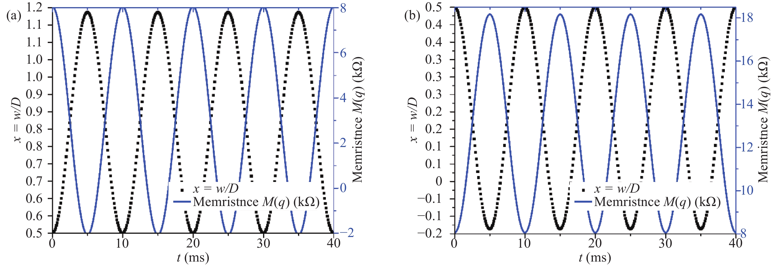
Fig. 4.  (Color online) Excess growth of conductive thickness and the corresponding memristance from their limiting value for RON = 100 Ω, ROFF = 16 kΩ, winitial = 5 nm, µv = 10−14 m2/(V·s), at v(t) = 2 V sinusoidal and 100 Hz (a) in saturation {x→1, M(q)→100 Ω} and (b) in depletion {x→0, M(q)→16 kΩ}.

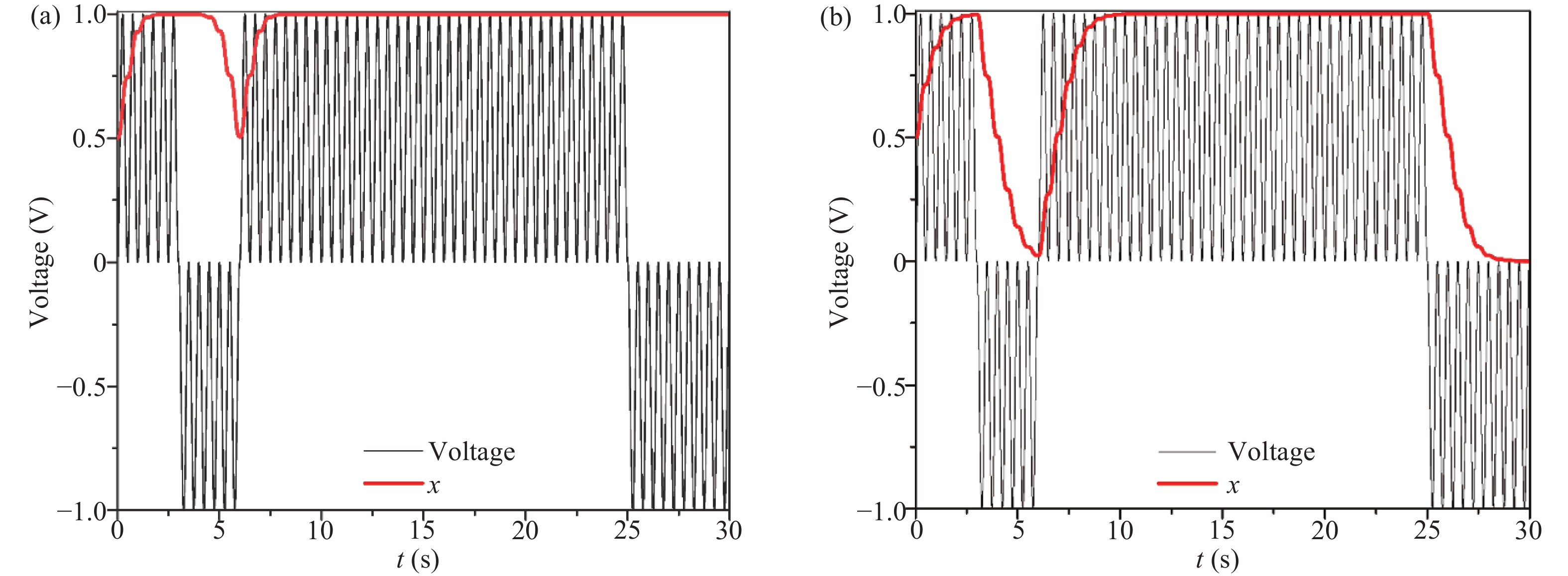
Fig. 5.  (Color online) (a) Boundary locked: state variable does not change its state as the polarity of applied voltage changes using Jogelkar’s window. (b) Boundary unlocked: state variable changes its states as the polarity of applied voltage changes for Biolek’s window function.

Fig. 6.  (Color online) Prodromakis’s window function limits the boundaries growth within the device’s physical limit and includes non-linearity at the (a) saturation and (b) depletion boundaries in the linear memristor model for the same parameters used in Fig. 4.

Fig. 7.  (Color online) (a) Memristor device structure and (b) its equivalent non-linear circuit[31].

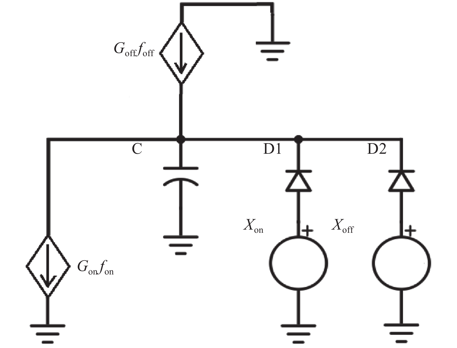
Fig. 8.  (a) Memristor device structure of the Simmons tunnel model[34]. (b) Spice modeling of Simmons tunnel’s tunneling width by capacitor and state variable derivatives for OFF and ON switching by current sources Goff and Gon[35].

Fig. 9.  Different work function of two metal electrodes resulting in a trapezoidal barrier in thin insulating film[36].

Fig. 10.  Micro spice TEAM model[38].

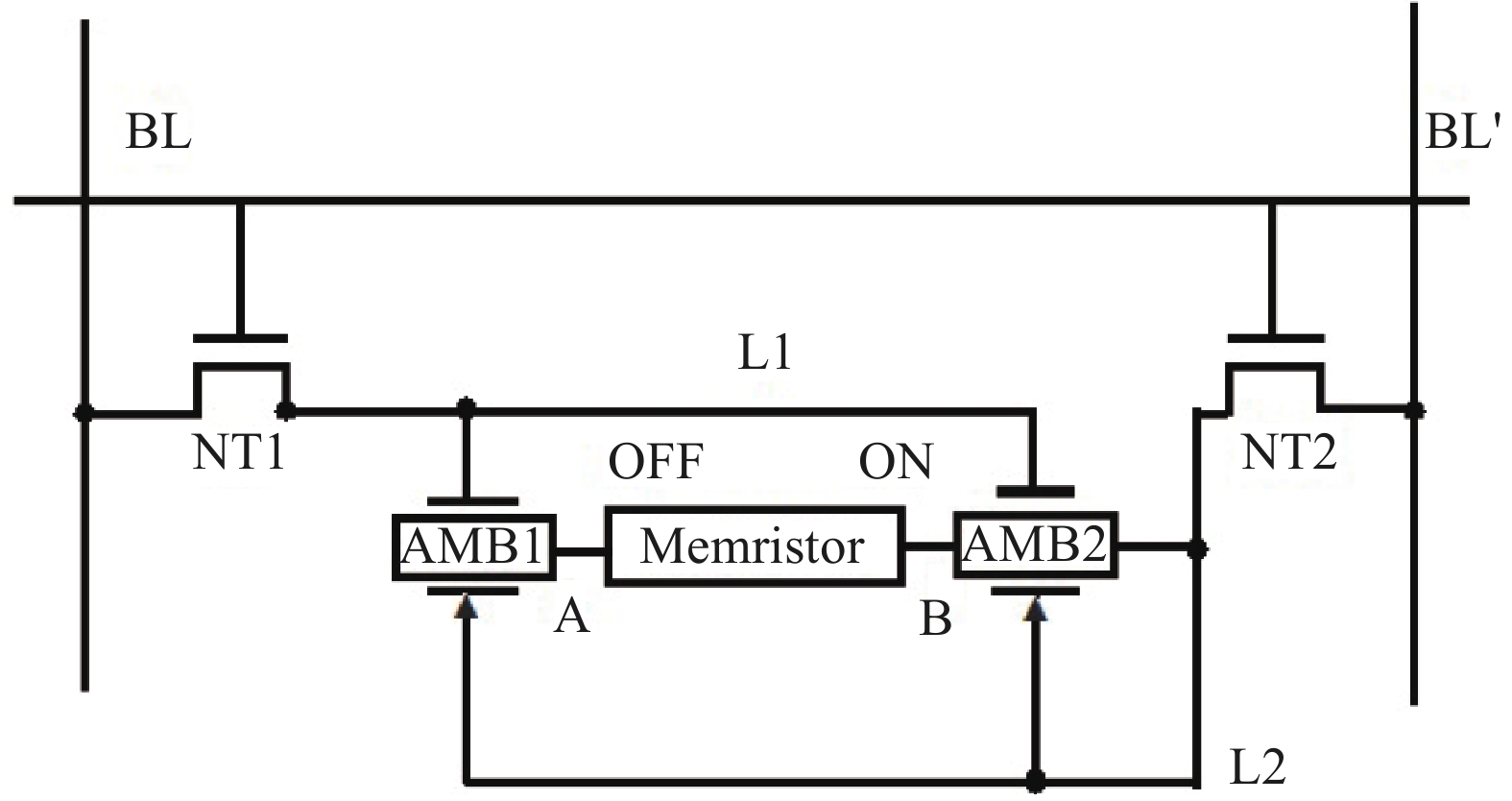
Fig. 11.  Hybrid memory cell exploiting a memristor and two ambipolar transistors[54].

Fig. 12.  (a) Variation of the write time of hybrid memory cell for a range of memristance. (b) Consecutive Write ‘1’ and Write ‘0’ operation with changing memristance values.

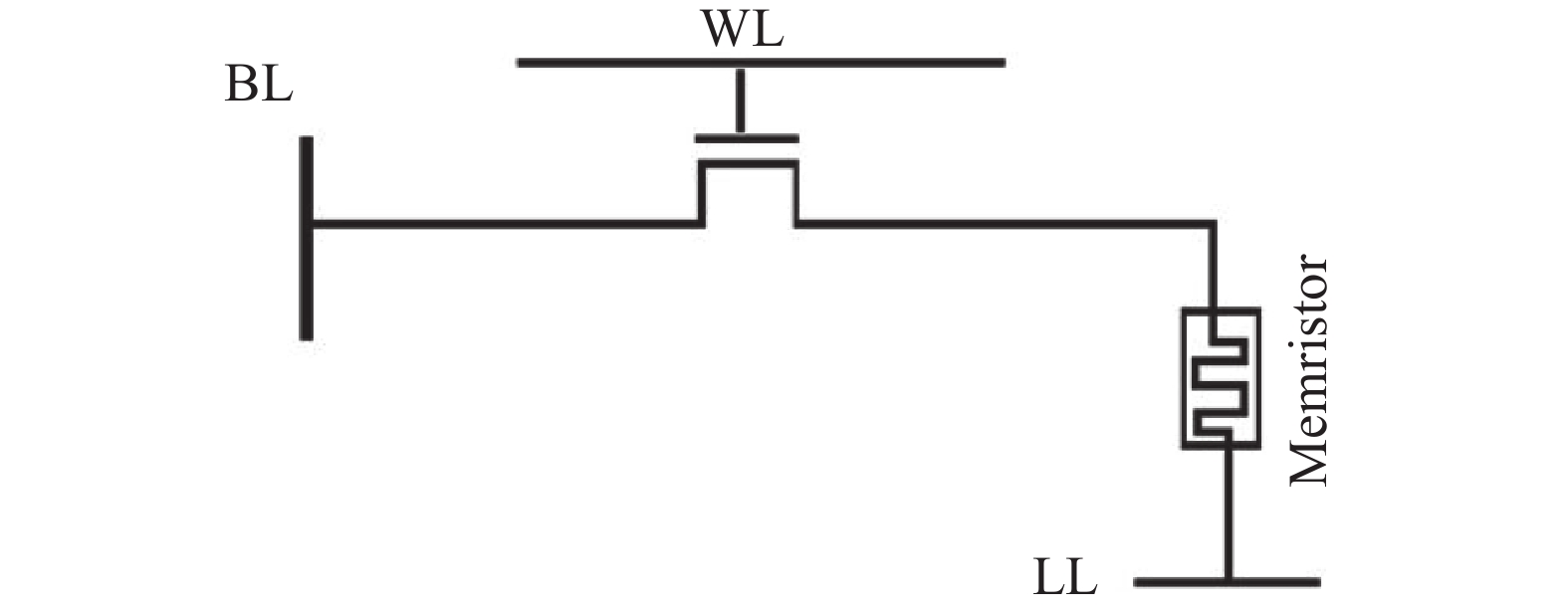
Fig. 13.  Unit 1T1R cell of array structure[56].

Fig. 14.  (Color online) Energy consumption in several components of TiO2 based RRAM array for multiple (n) bit storage during (a) write operation, and (b) read operation.

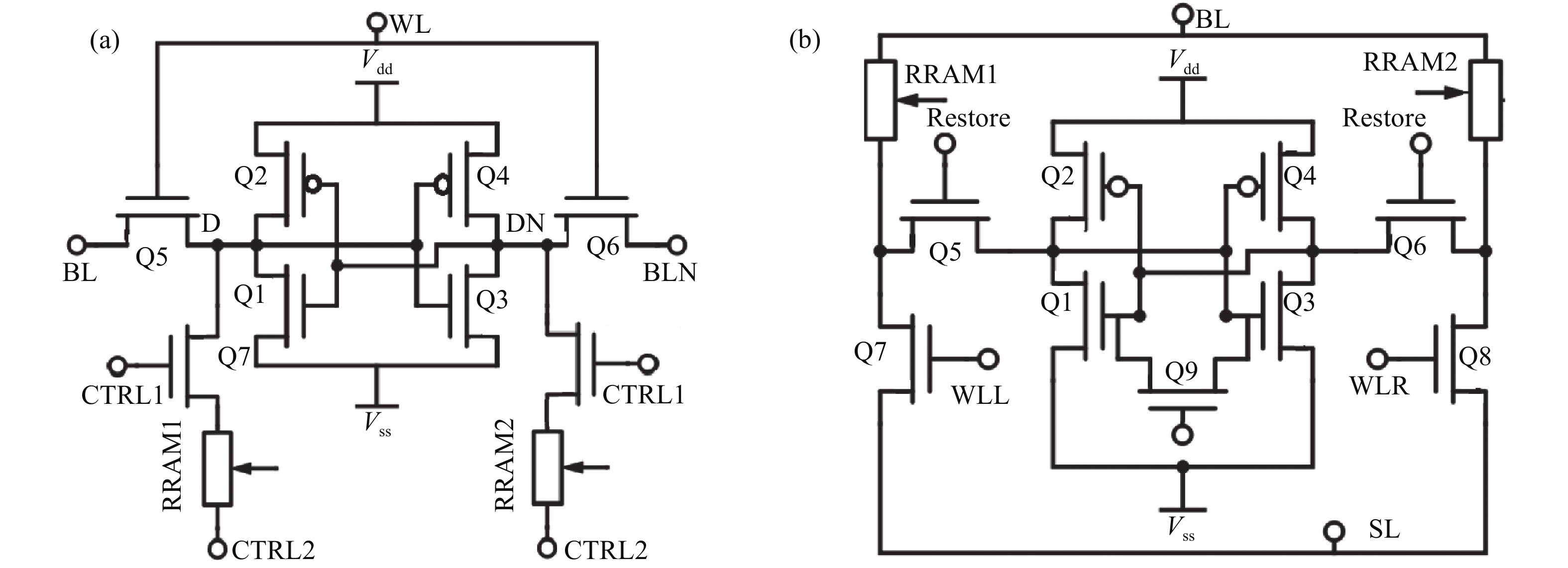
Fig. 15.  (Color online) (a) Basic structure of 7T1R SRAM[57]. (b) WSNM of 7T1R SRAM for storing ‘0’. (c) WSNM of 7T1R SRAM for storing ‘1’.

Fig. 16.  More configurations of SRAM utilizing memristor. (a) 8T2R SRAM[58]. (b) 9T2R SRAM[59].

Fig. 17.  (Color online) (a) Average read delay, (b) average write delay of various considered SRAM cells configuration with different feature size.

Table 1.   Description of four fundamental circuit elements.

S.No Circuit element Inventor Invention year Relating parameter Relation Symbol
1 Capacitor Ewald George Von Kleist 1745 Charge (q) and voltage (v) dq = Cdv
2 Resistor George Simon Ohm 1827 Voltage (v) and current (i) dv = Rdi
3 Inductor Michael Faraday 1831 Magnetic flux (φ) and current dφ = Ldi
4 Memristor Leon Chua 1971 Magnetic flux (ϕ) and charge (q) dφ = Mdq
5 Basic law of electricity Charge and current $q\left( t \right) = \mathop \smallint \limits_{ - \infty }^t i\left( \tau \right){\rm{d}}\tau $ or $i = \frac{{{\rm{d}}q}}{{{\rm{d}}t}}$
6 Basic law of magnetism Flux and voltage $\varphi \left( t \right) = \mathop \smallint \limits_{ - \infty }^t v\left( \tau \right){\rm{d}}\tau $ or $v = \frac{{{\rm{d}}\varphi }}{{{\rm{d}}t}}$
DownLoad: CSV

Table 2.   Comparison of hybrid memory cell with NAND/NOR flash.

Parameter Hybrid memory cell NAND flash[55] NOR flash[55]
Write time (ns) 21 106 103
Read time (ns) 1.095 105 15
Write operating voltage (V) 0.9 15 15
Read operating
voltage (V)
0.9 1.8 1.8
DownLoad: CSV

Table 3.   Comparison of various parameters of existing memory structures extracted from[12, 56] .

Parameter Traditional memories Other emerging technologies
DRAM SRAM NOR FLASH NAND FLASH FeRAM MRAM PCRAM STTRAM MEMRISTOR
Cell element 1T1C 6T 1T 1T 1T1C 1T1R 1T1R 1T1R 1T1R
Feature size (nm) 36–65 45 90 22 180 65 45 40 9
Density (Gbit/cm2) 0.8–13 0.4 1.2 52 0.14 1.2 12 15 154–309
Read time (ns) 2–10 0.2 15 100 45 35 12 35 8.5
Write time (ns) 2–10 0.2 107 106 65 35 100 35 10
Retention time 4–64 ms N/A 10 years 10 years 10 years > 10 years > 10 years > 10 years > 10 years
DownLoad: CSV
[1]
Baughman R H, Zakhidov A A, De Heer W A. Carbon nanotubes–the route toward applications. Science, 2002, 297(5582): 787 doi: 10.1126/science.1060928
[2]
Greytak A B, Lauhon L J, Gudiksen M S, et al. Growth and transport properties of complementary germanium nanowire field-effect transistors. Appl Phys Lett, 2004, 84(21): 4176 doi: 10.1063/1.1755846
[3]
Heyns M, Tsai W. Ultimate scaling of CMOS logic devices with Ge and III–V materials. Mrs Bulletin, 2009, 34(7): 485 doi: 10.1557/mrs2009.136
[4]
Knoch J, Appenzeller J. Modeling of high-performance p-type III–V heterojunction tunnel FETs. IEEE Electron Device Lett, 2010, 31(4): 305 doi: 10.1109/LED.2010.2041180
[5]
Salahuddin S, Datta S. Use of negative capacitance to provide voltage amplification for low power nanoscale devices. Nano Lett, 2008, 8(2): 405 doi: 10.1021/nl071804g
[6]
Schliemann J, Egues J C, Loss D. Nonballistic spin-field-effect transistor. Phys Rev Lett, 2003, 90(14): 146801 doi: 10.1103/PhysRevLett.90.146801
[7]
Jang W W, Yoon J B, Kim M S, et al. NEMS switch with 30 nm-thick beam and 20 nm-thick air-gap for high density non-volatile memory applications. Solid-State Electron, 2008, 52(10): 1578 doi: 10.1016/j.sse.2008.06.026
[8]
International Technology Roadmap for Semiconductor 2.0, executive report, 2015
[9]
Qazi M, Clinton M, Bartling S. A low-voltage 1 Mb FRAM in 0.13 μm CMOS featuring time-to-digital sensing for expanded operating margin. IEEE J Solid-State Circuits, 2012, 47(1): 141 doi: 10.1109/JSSC.2011.2164732
[10]
Waser R. Nanotechnology: volume 4: information technology II. Weinheim: John Wiley & Sons, 2008
[11]
Wong H S, Raoux S, Kim S, et al. Phase change memory. Proc IEEE, 2010, 98(12): 2201 doi: 10.1109/JPROC.2010.2070050
[12]
Wang K L, Alzate J G, Amiri P K. Low-power non-volatile spintronic memory: STT-RAM and beyond. J Phys D, 2013, 46(7): 074003 doi: 10.1088/0022-3727/46/7/074003
[13]
Lee M J, Lee C B, Lee D, et al. A fast, high-endurance and scalable non-volatile memory device made from asymmetric Ta2O5−x/TaO2−x bilayer structures. Nat Mater, 2011, 10(8): 625 doi: 10.1038/nmat3070
[14]
Chua L. Memristor—the missing circuit element. IEEE Trans Circuit Theory, 1971, 18(5): 507 doi: 10.1109/TCT.1971.1083337
[15]
Oster G. A note on memristors. IEEE Trans Circuits Syst, 1974, 21(1): 152
[16]
Chua L O, Kang SM. Memristive devices and systems. Proc IEEE, 1976, 64(2): 209 doi: 10.1109/PROC.1976.10092
[17]
Adhikari S P, Sah M P, Kim H, et al. Three fingerprints of memristor. IEEE Trans Circuits Syst I, 2013, 60(11): 3008 doi: 10.1109/TCSI.2013.2256171
[18]
Chua L. Device modeling via nonlinear circuit elements. IEEE Trans Circuits Syst, 1980, 27(11): 1014 doi: 10.1109/TCS.1980.1084742
[19]
Di Ventra M, Pershin Y V, Chua L O. Circuit elements with memory: memristors, memcapacitors, and meminductors. Proc IEEE, 2009, 97(10): 1717 doi: 10.1109/JPROC.2009.2021077
[20]
Strukov D B, Snider G S, Stewart D R, et al. The missing memristor found. Nature, 2008, 453(7191): 80 doi: 10.1038/nature06932
[21]
Raj B, Vaidyanathan S. Advances in memristors, memristive devices and systems. Springer International Publishing, 2017, 701: 449
[22]
Blanc J, Staebler D L. Electrocoloration in SrTiO3: vacancy drift and oxidation-reduction of transition metals. Phys Rev B, 1971, 4(10): 3548 doi: 10.1103/PhysRevB.4.3548
[23]
Bansal P, Raj B. Memristor modeling and analysis for linear dopant drift kinetics. J Nanoeng Nanomanuf, 2016, 6(4): 306 doi: 10.1166/jnan.2016.1296
[24]
Strukov D B, Williams R S. Exponential ionic drift: fast switching and low volatility of thin-film memristors. Appl Phys A, 2009, 94(3): 515 doi: 10.1007/s00339-008-4975-3
[25]
Joglekar Y N, Wolf S J. The elusive memristor: properties of basic electrical circuits. Eur J Phys, 2009, 30(4): 661 doi: 10.1088/0143-0807/30/4/001
[26]
Bansal P, Raj B. Memristor: a versatile nonlinear model for dopant drift and boundary issues. J Comput Theor Nanosci, 2017, 14(5): 2319 doi: 10.1166/jctn.2017.6827
[27]
Biolek Z, Biolek D, Biolkova V. SPICE model of memristor with nonlinear dopant drift. Radioengineering, 2009, 18(2): 210
[28]
Prodromakis T, Peh B P, Papavassiliou C, et al. A versatile memristor model with nonlinear dopant kinetics. IEEE Trans Electron Devices, 2011, 58(9): 3099 doi: 10.1109/TED.2011.2158004
[29]
Zha J, Huang H, Liu Y. A novel window function for memristor model with application in programming analog circuits. IEEE Trans Circuits Syst II, 2016, 63(5): 423 doi: 10.1109/TCSII.2015.2505959
[30]
Singh J, Raj B. Frequency dependent window function for stochastic nature of memristor model. 4th International Conference on Production and Industrial Engineering, CPIE, 2016: 19
[31]
Yang J J, Pickett M D, Li X, et al. Memristive switching mechanism for metal/oxide/metal nanodevices. Nat Nanotechnol, 2008, 3(7): 429 doi: 10.1038/nnano.2008.160
[32]
Simmons J G. Generalized formula for the electric tunnel effect between similar electrodes separated by a thin insulating film. J Appl Phys, 1963, 34(6): 1793 doi: 10.1063/1.1702682
[33]
Simmons J G. Electric tunnel effect between dissimilar electrodes separated by a thin insulating film. J Appl Phys, 1963, 34(9): 2581 doi: 10.1063/1.1729774
[34]
Pickett M D, Strukov D B, Borghetti J L, et al. Switching dynamics in titanium dioxide memristive devices. J Appl Phys, 2009, 106(7): 074508 doi: 10.1063/1.3236506
[35]
Abdalla H, Pickett M D. SPICE modeling of memristors. 2011 IEEE International Symposium on Circuits and Systems (ISCAS), 2011: 1832
[36]
Hassan A M, Fahmy H A, Rafat N H. Enhanced model of conductive filament-based memristor via including trapezoidal electron tunneling barrier effect. IEEE Trans Nanotechnol, 2016, 15(3): 484 doi: 10.1109/TNANO.2016.2546686
[37]
Yakopcic C, Taha T M, Subramanyam G, et al. A memristor device model. IEEE Electron Device Lett, 2011, 32(10): 1436 doi: 10.1109/LED.2011.2163292
[38]
Kvatinsky S, Friedman E G, Kolodny A, et al. TEAM: threshold adaptive memristor model. IEEE Trans Circuits Syst I, 2013, 60(1): 211 doi: 10.1109/TCSI.2012.2215714
[39]
Kvatinsky S, Ramadan M, Friedman E G, et al. VTEAM: a general model for voltage-controlled memristors. IEEE Trans Circuits Syst II, 2015, 62(8): 786 doi: 10.1109/TCSII.2015.2433536
[40]
Rák Á, Cserey G. Macromodeling of the memristor in SPICE. IEEE Trans Compur-Aid Des Integr Circuits Syst, 2010, 29(4): 632 doi: 10.1109/TCAD.2010.2042900
[41]
Pershin Y V, Di Ventra M. SPICE model of memristive devices with threshold. arXiv preprint arXiv: 1204.2600, 2012
[42]
Biolek D, Di Ventra M, Pershin Y V. Reliable SPICE simulations of memristors, memcapacitors and meminductors. arXiv preprint arXiv: 1307.2717, 2013
[43]
Vourkas I, Batsos A, Sirakoulis G C. SPICE modeling of nonlinear memristive behavior. Int J Circuit Theory Appl, 2015, 43(5): 553 doi: 10.1002/cta.v43.5
[44]
Liu C, Yang Q, Zhang C, et al. A memristor-based neuromorphic engine with a current sensing scheme for artificial neural network applications. 22nd Asia and South Pacific on Design Automation Conference (ASP-DAC), 2017: 647
[45]
Muthuswamy B, Kokate P P. Memristor-based chaotic circuits. IETE Tech Rev, 2009, 26(6): 417 doi: 10.4103/0256-4602.57827
[46]
Kvatinsky S, Kolodny A, Weiser U C, et al. Memristor-based IMPLY logic design procedure. IEEE 29th International Conference on Computer Design (ICCD), 2011: 142
[47]
Wey T A, Jemison W D. Variable gain amplifier circuit using titanium dioxide memristors. IET Circuits, Devices Syst, 2011, 5(1): 59 doi: 10.1049/iet-cds.2010.0210
[48]
Bao B C, Liu Z, Xu J P. Steady periodic memristor oscillator with transient chaotic behaviours. Electron Lett, 2010, 46(3): 237
[49]
Talukdar A, Radwan A G, Salama K N. Generalized model for memristor-based Wien family oscillators. Microelectron J, 2011, 42(9): 1032 doi: 10.1016/j.mejo.2011.07.001
[50]
Chandra S. On the discovery of a polarity-dependent memory switch and/or memristor (memory resistor). IETE Techl Rev, 2010, 27(2): 179 doi: 10.4103/0256-4602.60170
[51]
Kim H, Sah M P, Yang C, et al. Memristor-based multilevel memory. 2010 12th international workshop on Cellular Nanoscale Networks and Their Applications (CNNA), 2010: 1
[52]
Robinett W, Pickett M, Borghetti J, et al. A memristor-based nonvolatile latch circuit. Nanotechnology, 2010, 21(23): 235203 doi: 10.1088/0957-4484/21/23/235203
[53]
Waser R, Dittmann R, Staikov G, et al. Redox-based resistive switching memories–nanoionic mechanisms, prospects, and challenges. Adv Mater, 2009, 21(25/26): 2632
[54]
Junsangsri P, Lombardi F. Design of a hybrid memory cell using memristance and ambipolarity. IEEE Trans Nanotechnol, 2013, 12(1): 71 doi: 10.1109/TNANO.2012.2229715
[55]
International Technology Roadmap for Semiconductors (ITRS). [Online]. Available: www.itrs.net/Links/2011ITRS/ 2011Chapters/2011ERD, 2011: 6.
[56]
Zangeneh M, Joshi A. Design and optimization of nonvolatile multibit 1T1R resistive RAM. IEEE Trans Very Large Scale Integr (VLSI) Syst, 2014, 22(8): 1815 doi: 10.1109/TVLSI.2013.2277715
[57]
Wei W, Namba K, Han J, et al. Design of a nonvolatile 7T1R SRAM cell for instant-on operation. IEEE Trans Nanotechnol, 2014, 13(5): 905 doi: 10.1109/TNANO.2014.2329915
[58]
Turkyilmaz O, Onkaraiah S, Reyboz M, et al. RRAM-based FPGA for " Normally Off, Instantly On” applications. Journal of Parallel and Distributed Computing, 2014, 74(6): 2441 doi: 10.1016/j.jpdc.2013.08.003
[59]
Xue X, Jian W, Xie Y, et al. Novel RRAM programming technology for instant-on and high-security FPGAs. 2011 IEEE 9th International Conference on ASIC (ASICON), 2011: 291
[60]
Wang J, Nalam S, Calhoun B H. Analyzing static and dynamic write margin for nanometer SRAMs. Proceedings of the 2008 International Symposium on Low Power Electronics & Design, 2008: 129
  • Search

    Advanced Search >>

    GET CITATION

    shu

    Export: BibTex EndNote

    Article Metrics

    Article views: 5916 Times PDF downloads: 219 Times Cited by: 0 Times

    History

    Received: 17 August 2017 Revised: 23 October 2017 Online: Accepted Manuscript: 04 April 2018Uncorrected proof: 12 April 2018Published: 01 July 2018

    Catalog

      Email This Article

      User name:
      Email:*请输入正确邮箱
      Code:*验证码错误
      Jeetendra Singh, Balwinder Raj. Comparative analysis of memristor models and memories design[J]. Journal of Semiconductors, 2018, 39(7): 074006. doi: 10.1088/1674-4926/39/7/074006 ****J Singh, B Raj, Comparative analysis of memristor models and memories design[J]. J. Semicond., 2018, 39(7): 074006. doi: 10.1088/1674-4926/39/7/074006.
      Citation:
      Jeetendra Singh, Balwinder Raj. Comparative analysis of memristor models and memories design[J]. Journal of Semiconductors, 2018, 39(7): 074006. doi: 10.1088/1674-4926/39/7/074006 ****
      J Singh, B Raj, Comparative analysis of memristor models and memories design[J]. J. Semicond., 2018, 39(7): 074006. doi: 10.1088/1674-4926/39/7/074006.

      Comparative analysis of memristor models and memories design

      doi: 10.1088/1674-4926/39/7/074006
      More Information
      • Corresponding author: jeetendras15.phd@nitj.ac.in, rajb@nitj.ac.in
      • Received Date: 2017-08-17
      • Revised Date: 2017-10-23
      • Published Date: 2018-07-01

      Catalog

        /

        DownLoad:  Full-Size Img  PowerPoint
        Return
        Return