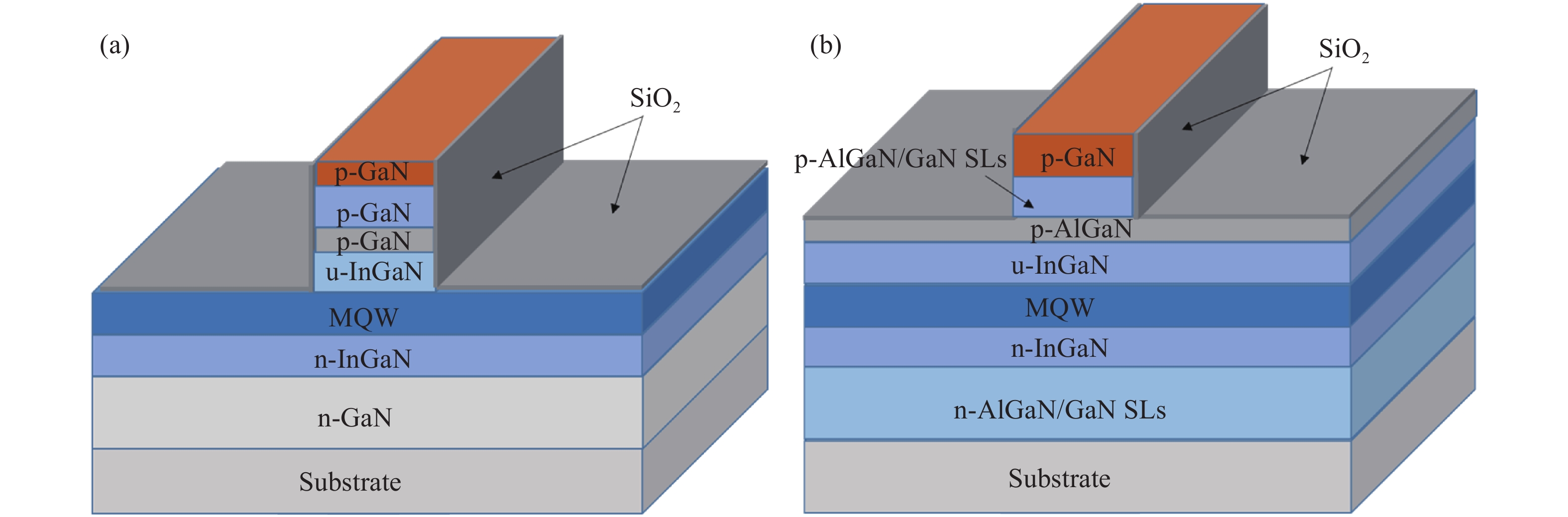
J. Semicond. > 2018, Volume 39 > Issue 8 > 084004

SEMICONDUCTOR DEVICES

Al-free cladding-layer blue laser diodes with a low aspect ratio in far-field beam pattern

Meixin Feng1, Qian Sun1, 2, , Jianping Liu1, 2, , Zengcheng Li1, Yu Zhou1, Hongwei Gao1, Shuming Zhang1, 2 and Hui Yang1, 2

+ Author Affiliations

 Corresponding author: Qian Sun, qsun2011@sinano.ac.cn (Sun Q); Jianping Liu, jpliu2010@sinano.ac.cn (Liu J P)

DOI: 10.1088/1674-4926/39/8/084004

PDF

Turn off MathJax

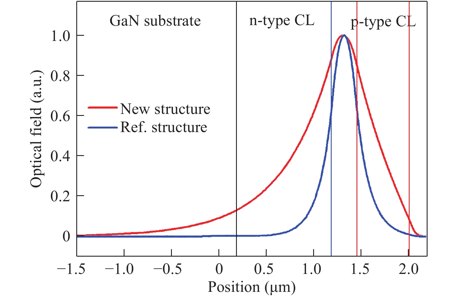
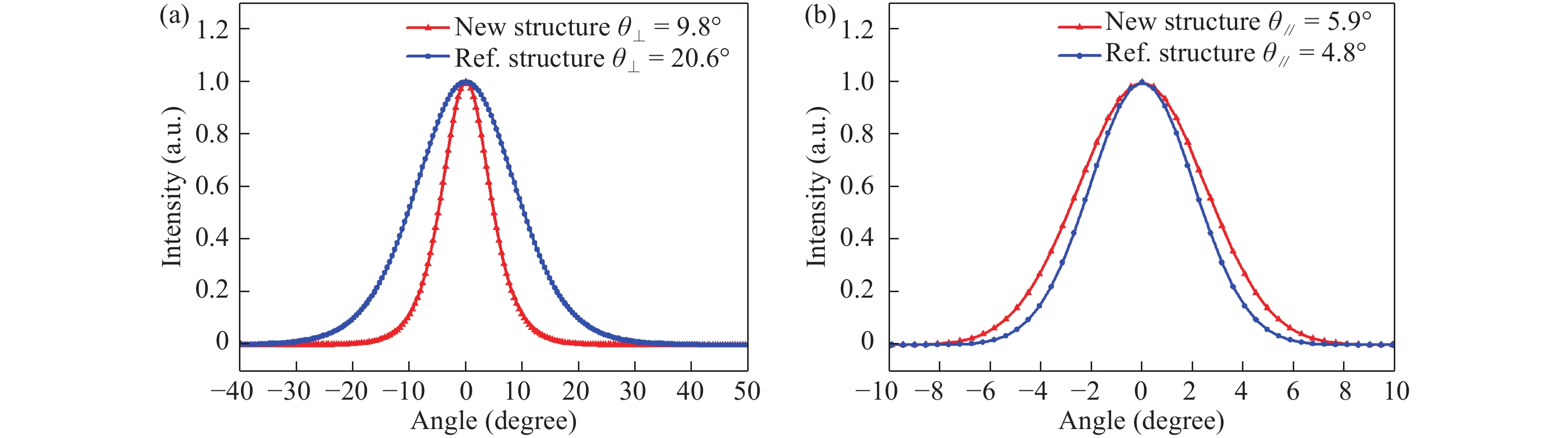
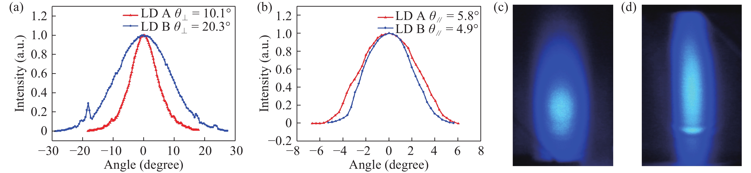
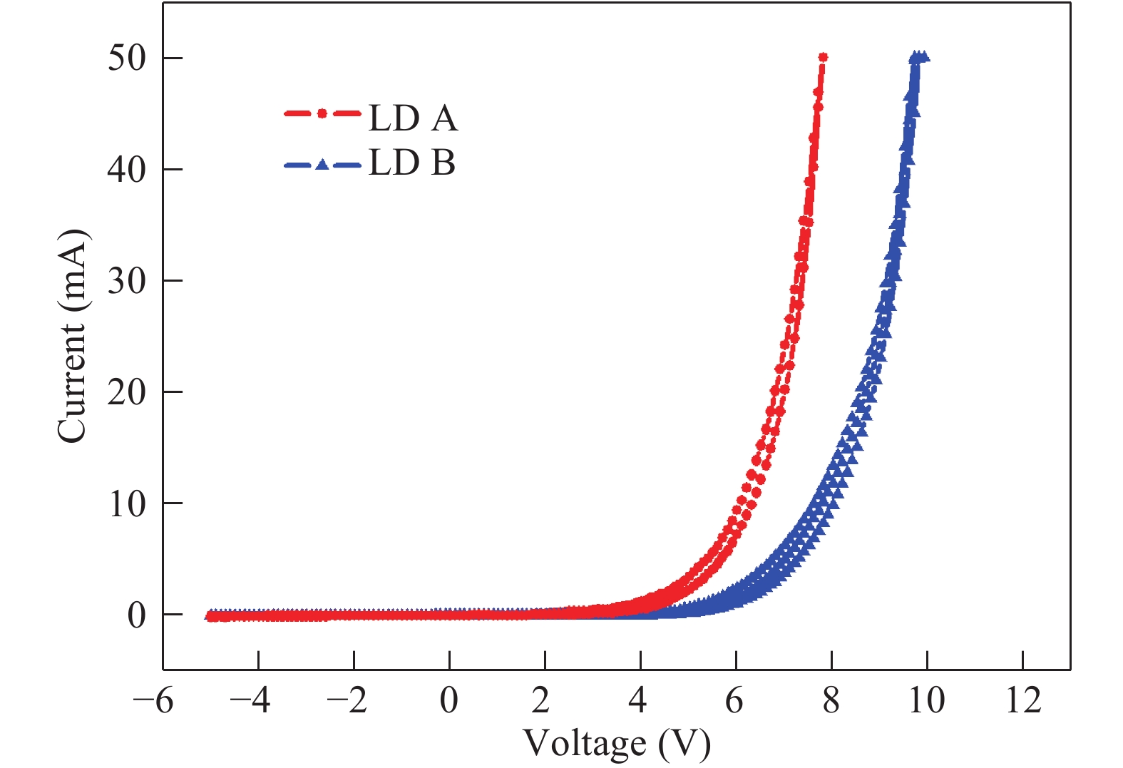
Abstract: c-plane GaN-based blue laser diodes (LDs) were fabricated with Al-free cladding layers (CLs) and deepened etching depth of mesa structure, so the aspect ratio of the far-field pattern (FFP) of the laser beam can be reduced to as low as 1.7, which is nearly the same as conventional AlGaInP-based red LDs. By using GaN CLs, the radiation angle of the laser beam θ is only 10.1° in the direction perpendicular to the junction plane. After forming a deeply etched mesa, the beam divergence angle parallel to the junction plane of FFP, θ//, increases from 4.9° to 5.8°. After using the modified structure, the operation voltage of LD is effectively reduced by 2 V at an injection current of 50 mA, but the threshold current value increases. The etching damage may be one of the main reasons responsible for the increase of the threshold current.

Key words: Al-free cladding layersfar-field beam patternsaspect ratiolaser diodes

III-nitride semiconductor laser diodes (LDs) have attracted a great deal of attention and made remarkable progress in the last few years due to their great potential in laser lighting, communication systems, and laser display applications[13].

One of the emphasizing points for the widespread applications of these LDs as a promising light source, for example, used for the disk reading and writing, is to control the shape of beam spot, particularly to reduce the aspect ratio of the far-field pattern (FFP)[46]. A high aspect ratio deteriorates the coupling efficiency of the laser beam to the lens. However, the light emitted from GaN-based LDs is typically very elliptical. Normally, the FFP aspect ratio of GaN-based LDs is larger than 3[2, 7], which is nearly twice of that for conventional AlGaInP-based red LDs[8]. The reported θ for GaN-based LDs was usually larger than 20°[4, 5, 7, 9], while a smaller radiation angle of 16.5° was reported for conventional AlGaInP-based red LDs[8]. In order to reduce the aspect ratio of GaN-based LDs, it is necessary to decrease the radiation angle of the laser beam in the direction perpendicular to the junction plane (θ) and increase the beam divergence angle parallel to the junction plane (θ//). In fact, Asano et al. have changed the thickness of waveguide layers in GaN-based LDs to reduce the θ. However, it remains still as large as around 20° as reported in Refs. [4, 5].

For GaN-based LDs grown on bulk GaN substrates, the refractive index of the substrate is larger than that of AlGaN cladding layers (CLs). The waveguide mode may leak into the GaN substrate, which affects the FFP and threshold current. To solve this problem, the AlGaN cladding layers are required to be thicker[1012]. These strained AlGaN layers introduce several significant drawbacks, including increased possibility of cracking due to tensile strain, a higher operation voltage, and a poor structural quality. Furthermore, a thick AlGaN layer growth by metal-organic chemical vapor deposition (MOCVD) could be problematic for reactor stability due to parasitic reactions of the Al-containing precursor. Previous studies of high-power GaN-based LDs had shown that reducing the Al composition in the AlGaN CLs could increase the level of catastrophic optical damage. It is noted that to overcome these problems, non-polar or semi-polar GaN-based Al-free cladding-layer LDs were reported in the literature[1316]. However, till now the c-plane Al-free cladding-layer LDs have not been reported.

In this paper, we have numerically investigated the effects of Al-free CLs on θ of FFP and the deeply etched mesa on θ// of FFP for c-plane GaN-based blue LDs. After that, we also fabricated Al-free cladding-layer blue LDs with deeply etched mesa. The obtained aspect ratio of FFP is reduced to as low as 1.7, which is nearly the same as the value for conventional AlGaInP -based red LDs.

To examine the aspect ratio of FFP, the simulation of two selected laser structures, as shown in Figs. 1(a) and 1(b), is performed. The Al-free cladding-layer blue LD structure with deeply etched mesa (marked later as the new structure), as shown in Fig. 1(a), is composed of a 100-μm-thick n-type GaN substrate, a 1-μm-thick n-type GaN CL, a 120-nm-thick n-type In0.03Ga0.97N lower waveguide layer, the multi-quantum-well (MQW) active region, an 80-nm-thick unintentionally doped In0.03Ga0.97N upper waveguide layer, a 20-nm-thick heavily-doped p-type GaN electron blocking layer (EBL), a 500-nm-thick p-type GaN CL, and a 40-nm-thick heavily-doped p-type GaN contact layer. The MQW consists of three 2.5-nm-thick unintentionally doped In0.17Ga0.83N well layers and four 14-nm-thick n-type GaN barrier layers. For the purpose of comparison, a reference structure (marked later as reference structure), as shown in Fig. 1(b), is also calculated. The difference between it and the new structure is in the n-type CL, p-type CL and EBL. In the new structure, all n-type CL, p-type CL and p-type EBL are made of GaN, while in the reference structure, both n-type and p-type CLs are made of Al0.14Ga0.86N/GaN superlattices (SLs), and the EBL is made of p-type Al0.2Ga0.8N. Actually, the reference structure is a conventional structure and its performance has been reported many times in the literature[17, 18].

Figure  1.  (Color online) The schematic diagrams of (a) new structure and (b) reference structure.

The cavity lengths and the ridge widths for both the reference and new structures are 800 and 3.5 μm, respectively. The ridge depths are different and schematically shown in Fig. 1. For the new structure, the ridge depth is as deep as 640 nm, which is down to the MQW to enhance the confinement of optical field and current in the horizontal direction[19]. For the reference structure, the ridge depth is 540 nm, where both of p-type AlGaN/GaN SL CL and p-type GaN contact layer are etched away outside of the ridge. In simulation, the data of the refractive index are taken to be the same as those reported in previous studies[17]. Based on these refractive indexes, the 2-dimensional optical mode and FFP of two GaN-based LDs are calculated and analyzed by the commercial software Mode-Solution.

Fig. 2 shows the calculated optical field intensity distribution for both the reference and new structures in the direction perpendicular to the junction plane. For the reference structure, the maximum value of the optical field is in the MQW region. As the distance away from the MQW increases, the optical field intensity reduces gradually, and comes to nearly zero in both p-type and n-type CLs. The optical confinement in the active region is quite strong, and most of the optical field is distributed in the MQW and waveguide layer regions, which means that the θ of FFP for the reference structure is as large as 20.6°, as shown in Fig. 3(a). For the new structure with GaN CLs, the optical confinement in the active region is reduced a lot as compared with the reference structure. The maximum value of the optical field is still in the MQW, but it distributes in a much wider area, and spreads a little into the thick GaN substrate. According to the laser theory, the FFP of LDs is the diffraction pattern of the near-field pattern, and a larger optical field distribution area will induce smaller FFP. Therefore, the θ of FFP for the new structure is as small as 9.8°, which is less than half of the θ of FFP for the reference structure. Fig. 3(b) shows the calculated far-field intensity distribution of both the reference and new structures in the direction parallel to the junction plane (θ//). By increasing the etching depth of mesa, the optical confinement in the ridge of the new structure is enhanced, and the θ// is increased from 4.8° to 5.9° in comparison with the reference structure. Thus the aspect ratio of FFP for the new structure is 1.7, which is only nearly 39% of the reference structure and almost equal to that of the reported value for conventional AlGaInP-based red LDs.

Figure  2.  (Color online) The calculated optical field distribution for both reference and new structures in the direction perpendicular to the junction plane.
Figure  3.  (Color online) The calculated far-field intensity distributions of both reference and new structures in the directions (a) perpendicular to the junction plane (θ) and (b) parallel to the junction plane (θ//).

To check the above-mentioned results, two blue LDs, i.e., LD A with the new structure and LD B with the reference structure, were fabricated. Both of them were grown on c-plane free-standing GaN substrate in a low-pressure MOCVD reactor. The ridge structure of LDs was formed by ion beam etching. SiO2 was used to isolate the ridge edges from the thick p-type electrode. Conventional Ni/Au and Ti/Al/Ti/Au metal schemes were used as p-electrode and n-electrode, respectively. The resonant cavity facets were made by cleavage and left uncoated. The electrical and luminescence characteristics of the devices were measured by on-bar probing. All measurements were taken at room temperature (25 °C).

Fig. 4(a) shows the measured far-field intensity distribution of both LD A and LD B in the direction perpendicular to the junction plane. The obtained θ values are almost the same as simulation results. For LD A with GaN CLs, the θ is reduced to be 10.1°, which is only 48% of that (20.3°) for LD B. The far-field intensity of LD B exhibits a narrow side lobe located at the angle of nearly −18°, which is due to the waveguide mode leaking into the bulk GaN substrate. It is known that as the refractive index of bulk GaN substrate is larger than that of AlGaN CL, the waveguide mode could leak into the bulk GaN substrate when the n side optical confinement is not strong enough. It is why normally a thicker n-type AlGaN CL or an AlGaN CL with higher Al composition are often suggested to be adopted[11]. For LD A with the new structure, both CLs and substrate are of GaN material, so their refractive indexes are all the same. Therefore, no clear leakage mode exists.

Fig. 4(b) shows the measured far-field intensity distribution of both LD A and LD B in the direction parallel to the junction plane. For LD B with the reference structure, the θ// is 4.9°. For LD A with the deeper etched mesa, the θ// increases to 5.8°, making the aspect ratio of FFP for LD A with the new structure decrease to 1.7, which is much smaller than the value of 4.1 for LD B with the reference structure. Figs. 4(c) and 4(d) show the photographs of FFP for LD A and LD B, respectively, which also proves a smaller aspect ratio of FFP for LD A.

Figure  4.  (Color online) The measured far-field intensity distributions of both LD A and LD B in the direction (a) perpendicular to the junction plane (θ) and (b) parallel to the junction plane (θ//), and the FFP photographs of (c) LD A and (d) LD B.

Fig. 5 shows the voltage-current curves of LD A and LD B. For LD A with the new structure, p-type GaN is used as the CL, and the operation voltage is 7.8 V at the injection current of 50 mA. On the other side, as the activation energy of the Mg acceptor increases with increasing Al composition of the p-AlGaN alloy[17], it has an influence on the conductivity of CLs. For LD B with p-type Al0.14Ga0.86N/GaN SL CL, the operation voltage is 9.8 V at the injection current of 50 mA, which is 2 V larger than that for LD A.

Figure  5.  (Color online) The voltage–current curves of LD A and LD B.

The measured pulsed power-current curves of LD A and LD B are shown in Fig. 6. The pulse width is 400 ns and the repetition rate is 10 kHz, which corresponds to a 4‰ duty cycle. For LD A with the new structure, the threshold current is 750 mA, which is much larger than that (~450 mA) of LD B with the reference structure. A possible reason for the difference could be explained as follows.

Figure  6.  (Color online) The power–current curves of LD A, LD B, and LD C.

(1) Optical confinement factor of the MQW region becomes smaller. Actually, compared with LD B, the optical confinement of the active region for LD A with the new structure is reduced, and the optical field is distributed in a much wider area, which decreases the optical confinement factor of the MQW. To make the LD lasing, the material gain of the LD should be increased, which would raise the threshold current.

(2) Absorption loss increases. Mg acceptor in the p-type region causes a strong absorption[20]. The optical loss of the LD mainly comes from the p-type region[21]. Due to there being less optical confinement in the active region of LD A, the optical field distributed in the p-type region increases. Therefore, the absorption loss for LD A is larger than that of LD B, which will increase the threshold current too.

(3) Etching damage. The etching process will cause a lot of etching damage, such as surface states, N vacancies, and so on[22, 23]. Such etching damage would become non-radiative recombination centers and influence the efficiency[19]. For LD A with deeply etched mesa, the current lateral spreading could be suppressed efficiently, and the optical confinement in the ridge is also enhanced. However, the etching damage is much closer to the MQW region where the peak optical field is located. Therefore, the non-radiative recombination due to etching damage will play a more important role, which would increase the threshold current.

To check the influence of etching depth, we have additionally fabricated another blue LD (named as LD C) with Al-free cladding layers by using the same wafer as LD A. The difference between LD A and LD C is in the etching depth. The etching depth for LD C is 540 nm, which is the same as LD B. As shown in Fig. 6, the threshold current of LD C is nearly 500 mA, which is a little larger than that of LD B (~450 mA), but much smaller than that of LD A (~750 mA). Therefore, it is shown that a smaller optical confinement factor and a larger absorption loss may play roles in the difference of threshold current for LD A and LD B, and the etching damage should be one of the main reasons responsible for that. To reduce the threshold current of LD A, the etching damage should be carefully removed or passivated. Therefore, a wet etching or passivation method is under way to remove or passivate the etching damage to significantly reduce the threshold current of LD A. Additionally, compared with LD B, the threshold current of LD C is only 11% larger, however, the operation voltage for LD A (or LD C) is 2 V less at the injection current of 50 mA (1.8 kA/cm2). Therefore, Al-free cladding-layer LDs could also play an important role in GaN-based high-power LDs.

In conclusion, we have made c-plane GaN-based blue LDs with Al-free cladding layers, emphasized on achieving the beam spot with a low aspect ratio of FFP. The LD structures with and without Al-free CLs are compared with each other by simulation and experiment. By using Al-free CLs, the θ of FFP is reduced from 20.3° to 10.1°. With deeper etched mesa, the θ// of FFP is increased from 4.9° to 5.8°. Therefore, the aspect ratio of FFP is reduced to be 1.7, which is almost the same as the reported value for conventional AlGaInP-based red LDs. The LD operation voltage at the injection current of 50 mA is also reduced by 2 V when using Al-free CLs. In addition, we analyzed the reasons causing the threshold current difference between LDs with and without Al-free CLs; the etching damage is found to be one of the main reasons.


[1]
Nakamura S, Senoh M, Nagahama S, et al. InGaN-based multi-quantum-well-structure laser diodes. Jpn J Appl Phys, 1996, 35: L74 doi: 10.1143/JJAP.35.L74
[2]
Nakamura S, Senoh M, Nagahama S, et al. High-power, long-lifetime InGaN/GaN/AlGaN based laser diodes grown on pure GaN substrates. Jpn J Appl Phys, 1998, 37: L309 doi: 10.1143/JJAP.37.L309
[3]
Kawaguchi M, Imafuji O, Nozaki S, et al. Optical-loss suppressed InGaN laser diodes using undoped thick waveguide structure. Proc SPIE, 2016, 9748: 974818 doi: 10.1117/12.2212011
[4]
Asano T, Takeya M, Tojyo T, et al. High-power 400-nm-band AlGaInN-based laser diodes with low aspect ratio. Appl Phys Lett, 2002, 80: 3497 doi: 10.1063/1.1478157
[5]
Asano T, Tojyo T, Mizuno T, et al. 100-mW kink-free blue-violet laser diodes with low aspect ratio. IEEE J Quantum Electr, 2003, 39: 135 doi: 10.1109/JQE.2002.806213
[6]
Ito S, Yamasaki Y, Omi S, et al. AlGaInN violet laser diodes grown on GaN substrates with low aspect ratio. Jpn J Appl Phys, 2004, 43: 96 doi: 10.1143/JJAP.43.96
[7]
Tojyo T, Asano T, Takeya M, et al. GaN-based high power blue-violet laser diodes. Jpn J Appl Phys, 2001, 40: 3206 doi: 10.1143/JJAP.40.3206
[8]
Hiroyama R, Inoue D, Nomura Y, et al. High-power 660-nm-band algainp laser diodes with a small aspect ratio for beam divergence. Jpn J Appl Phys, 2002, 41: 1154 doi: 10.1143/JJAP.41.1154
[9]
Ryu H Y, Ha K H, Lee S N, et al. High-performance blue InGaN laser diodes with single-quantum-well active layers. IEEE Photonic Tech L, 2007, 19: 1717 doi: 10.1109/LPT.2007.905215
[10]
Braun H, Lauterbach C, Schwarz U T, et al. Experimental and theoretical study of substrate modes in (Al,In)GaN laser diodes. Phys Status Solidi C, 2007, 4: 2772 doi: 10.1002/(ISSN)1610-1642
[11]
Laino V, Roemer F, Witzigmann B, et al. Substrate modes of (Al,In)GaN semiconductor laser diodes on SiC and GaN substrates. IEEE J Quantum Electr, 2007, 43: 16 doi: 10.1109/JQE.2006.884769
[12]
Lermer T, Schillgalies M, Breidenassel A, et al. Waveguide design of green InGaN laser diodes. Phys Status Solidi A, 2010, 207: 1328 doi: 10.1002/pssa.200983410
[13]
Feezell D F, Schmidt M C, Farrell R M, et al. AlGaN-cladding-free nonpolar InGaN/GaN laser diodes. Jpn J Appl Phys, 2007, 46: L284 doi: 10.1143/JJAP.46.L284
[14]
Farrell R M, Hsu P S, Haeger D A, et al. Low-threshold-current-density AlGaN-cladding-free m-plane InGaN/GaN laser diodes. Appl Phys Lett, 2010, 96: 2311132
[15]
Pourhashemi A, Farrell R M, Hardy M T, et al. Pulsed high-power AlGaN-cladding-free blue laser diodes on semipolar (20-21) GaN substrates. Appl Phys Lett, 2013, 103: 151112 doi: 10.1063/1.4824773
[16]
Tyagi A, Farrell R M, Kelchner K M, et al. AlGaN-cladding free green semipolar GaN based laser diode with a lasing wavelength of 506.4 nm. Appl Phys Express, 2010, 3: 011002 doi: 10.1143/APEX.3.011002
[17]
Feng M X, Liu J P, Zhang S M, et al. Design considerations for GaN-based blue laser diodes with InGaN upper waveguide layer. IEEE J Sel Topics Quantum Electron, 2013, 19: 1500705 doi: 10.1109/JSTQE.2012.2237015
[18]
Feng M X, Liu J P, Zhang S M, et al. High efficient GaN-based laser diodes with tunnel junction. Appl Phys Lett, 2013, 103: 043508 doi: 10.1063/1.4816598
[19]
Redaelli L, Martens M, Piprek J, et al. Effect of ridge waveguide etch depth on laser threshold of InGaN MQW laser diodes. Proc SPIE, 2012, 8262: 826219
[20]
Sizov D S, Bhat R, Heberle A, et al. Internal optical waveguide loss and p-type absorption in blue and green InGaN quantum well laser diodes. Appl Phys Express, 2010, 3: 122104 doi: 10.1143/APEX.3.122104
[21]
Huang C Y, Lin Y D, Tyagi A, et al. Optical waveguide simulations for the optimization of InGaN-based green laser diodes. J Appl Phys, 2010, 107: 023101 doi: 10.1063/1.3275325
[22]
Ladroue J, Meritan A, Boufnichel M, et al. Deep GaN etching by inductively coupled plasma and induced surface defects. J Vac Sci Technol A, 2010, 28: 1226 doi: 10.1116/1.3478674
[23]
Qiu R, Lu H, Chen D, et al. Optimization of inductively coupled plasma deep etching of GaN and etching damage analysis. Appl Surf Sci, 2011, 257: 2700 doi: 10.1016/j.apsusc.2010.10.048
Fig. 1.  (Color online) The schematic diagrams of (a) new structure and (b) reference structure.

Fig. 2.  (Color online) The calculated optical field distribution for both reference and new structures in the direction perpendicular to the junction plane.

Fig. 3.  (Color online) The calculated far-field intensity distributions of both reference and new structures in the directions (a) perpendicular to the junction plane (θ) and (b) parallel to the junction plane (θ//).

Fig. 4.  (Color online) The measured far-field intensity distributions of both LD A and LD B in the direction (a) perpendicular to the junction plane (θ) and (b) parallel to the junction plane (θ//), and the FFP photographs of (c) LD A and (d) LD B.

Fig. 5.  (Color online) The voltage–current curves of LD A and LD B.

Fig. 6.  (Color online) The power–current curves of LD A, LD B, and LD C.

[1]
Nakamura S, Senoh M, Nagahama S, et al. InGaN-based multi-quantum-well-structure laser diodes. Jpn J Appl Phys, 1996, 35: L74 doi: 10.1143/JJAP.35.L74
[2]
Nakamura S, Senoh M, Nagahama S, et al. High-power, long-lifetime InGaN/GaN/AlGaN based laser diodes grown on pure GaN substrates. Jpn J Appl Phys, 1998, 37: L309 doi: 10.1143/JJAP.37.L309
[3]
Kawaguchi M, Imafuji O, Nozaki S, et al. Optical-loss suppressed InGaN laser diodes using undoped thick waveguide structure. Proc SPIE, 2016, 9748: 974818 doi: 10.1117/12.2212011
[4]
Asano T, Takeya M, Tojyo T, et al. High-power 400-nm-band AlGaInN-based laser diodes with low aspect ratio. Appl Phys Lett, 2002, 80: 3497 doi: 10.1063/1.1478157
[5]
Asano T, Tojyo T, Mizuno T, et al. 100-mW kink-free blue-violet laser diodes with low aspect ratio. IEEE J Quantum Electr, 2003, 39: 135 doi: 10.1109/JQE.2002.806213
[6]
Ito S, Yamasaki Y, Omi S, et al. AlGaInN violet laser diodes grown on GaN substrates with low aspect ratio. Jpn J Appl Phys, 2004, 43: 96 doi: 10.1143/JJAP.43.96
[7]
Tojyo T, Asano T, Takeya M, et al. GaN-based high power blue-violet laser diodes. Jpn J Appl Phys, 2001, 40: 3206 doi: 10.1143/JJAP.40.3206
[8]
Hiroyama R, Inoue D, Nomura Y, et al. High-power 660-nm-band algainp laser diodes with a small aspect ratio for beam divergence. Jpn J Appl Phys, 2002, 41: 1154 doi: 10.1143/JJAP.41.1154
[9]
Ryu H Y, Ha K H, Lee S N, et al. High-performance blue InGaN laser diodes with single-quantum-well active layers. IEEE Photonic Tech L, 2007, 19: 1717 doi: 10.1109/LPT.2007.905215
[10]
Braun H, Lauterbach C, Schwarz U T, et al. Experimental and theoretical study of substrate modes in (Al,In)GaN laser diodes. Phys Status Solidi C, 2007, 4: 2772 doi: 10.1002/(ISSN)1610-1642
[11]
Laino V, Roemer F, Witzigmann B, et al. Substrate modes of (Al,In)GaN semiconductor laser diodes on SiC and GaN substrates. IEEE J Quantum Electr, 2007, 43: 16 doi: 10.1109/JQE.2006.884769
[12]
Lermer T, Schillgalies M, Breidenassel A, et al. Waveguide design of green InGaN laser diodes. Phys Status Solidi A, 2010, 207: 1328 doi: 10.1002/pssa.200983410
[13]
Feezell D F, Schmidt M C, Farrell R M, et al. AlGaN-cladding-free nonpolar InGaN/GaN laser diodes. Jpn J Appl Phys, 2007, 46: L284 doi: 10.1143/JJAP.46.L284
[14]
Farrell R M, Hsu P S, Haeger D A, et al. Low-threshold-current-density AlGaN-cladding-free m-plane InGaN/GaN laser diodes. Appl Phys Lett, 2010, 96: 2311132
[15]
Pourhashemi A, Farrell R M, Hardy M T, et al. Pulsed high-power AlGaN-cladding-free blue laser diodes on semipolar (20-21) GaN substrates. Appl Phys Lett, 2013, 103: 151112 doi: 10.1063/1.4824773
[16]
Tyagi A, Farrell R M, Kelchner K M, et al. AlGaN-cladding free green semipolar GaN based laser diode with a lasing wavelength of 506.4 nm. Appl Phys Express, 2010, 3: 011002 doi: 10.1143/APEX.3.011002
[17]
Feng M X, Liu J P, Zhang S M, et al. Design considerations for GaN-based blue laser diodes with InGaN upper waveguide layer. IEEE J Sel Topics Quantum Electron, 2013, 19: 1500705 doi: 10.1109/JSTQE.2012.2237015
[18]
Feng M X, Liu J P, Zhang S M, et al. High efficient GaN-based laser diodes with tunnel junction. Appl Phys Lett, 2013, 103: 043508 doi: 10.1063/1.4816598
[19]
Redaelli L, Martens M, Piprek J, et al. Effect of ridge waveguide etch depth on laser threshold of InGaN MQW laser diodes. Proc SPIE, 2012, 8262: 826219
[20]
Sizov D S, Bhat R, Heberle A, et al. Internal optical waveguide loss and p-type absorption in blue and green InGaN quantum well laser diodes. Appl Phys Express, 2010, 3: 122104 doi: 10.1143/APEX.3.122104
[21]
Huang C Y, Lin Y D, Tyagi A, et al. Optical waveguide simulations for the optimization of InGaN-based green laser diodes. J Appl Phys, 2010, 107: 023101 doi: 10.1063/1.3275325
[22]
Ladroue J, Meritan A, Boufnichel M, et al. Deep GaN etching by inductively coupled plasma and induced surface defects. J Vac Sci Technol A, 2010, 28: 1226 doi: 10.1116/1.3478674
[23]
Qiu R, Lu H, Chen D, et al. Optimization of inductively coupled plasma deep etching of GaN and etching damage analysis. Appl Surf Sci, 2011, 257: 2700 doi: 10.1016/j.apsusc.2010.10.048
1

Hot electron effects on the operation of potential well barrier diodes

M. Akura, G. Dunn, M. Missous

Journal of Semiconductors, 2019, 40(12): 122101. doi: 10.1088/1674-4926/40/12/122101

2

Rational molecular passivation for high-performance perovskite light-emitting diodes

Jingbi You

Journal of Semiconductors, 2019, 40(4): 040203. doi: 10.1088/1674-4926/40/4/040203

3

Thermal investigation of high-power GaAs-based laser diodes

Jichuan Liu, Cuiluan Wang, Suping Liu, Xiaoyu Ma

Journal of Semiconductors, 2017, 38(5): 054004. doi: 10.1088/1674-4926/38/5/054004

4

Fabrication of room temperature continuous-wave operation GaN-based ultraviolet laser diodes

Degang Zhao, Jing Yang, Zongshun Liu, Ping Chen, Jianjun Zhu, et al.

Journal of Semiconductors, 2017, 38(5): 051001. doi: 10.1088/1674-4926/38/5/051001

5

Thermal analysis in high power GaAs-based laser diodes

Xueqin Gong, Shiwei Feng, Yuan Yue, Junwei Yang, Jingwei Li, et al.

Journal of Semiconductors, 2016, 37(4): 044011. doi: 10.1088/1674-4926/37/4/044011

6

Suppression of electron leakage in 808 nm laser diodes with asymmetric waveguide layer

Xiang Li, Degang Zhao, Desheng Jiang, Ping Chen, Zongshun Liu, et al.

Journal of Semiconductors, 2016, 37(1): 014007. doi: 10.1088/1674-4926/37/1/014007

7

GaN-based green laser diodes

Lingrong Jiang, Jianping Liu, Aiqin Tian, Yang Cheng, Zengcheng Li, et al.

Journal of Semiconductors, 2016, 37(11): 111001. doi: 10.1088/1674-4926/37/11/111001

8

Influences of ICP etching damages on the electronic properties of metal field plate 4H-SiC Schottky diodes

Hui Wang, Yingxi Niu, Fei Yang, Yong Cai, Zehong Zhang, et al.

Journal of Semiconductors, 2015, 36(10): 104006. doi: 10.1088/1674-4926/36/10/104006

9

High power laser diodes of 2 μm AlGaAsSb/InGaSb type I quantum-wells

Yongping Liao, Yu Zhang, Junliang Xing, Sihang Wei, Hongyue Hao, et al.

Journal of Semiconductors, 2015, 36(5): 054007. doi: 10.1088/1674-4926/36/5/054007

10

A novel high performance ESD power clamp circuit with a small area

Yang Zhaonian, Liu Hongxia, Li Li, Zhuo Qingqing

Journal of Semiconductors, 2012, 33(9): 095006. doi: 10.1088/1674-4926/33/9/095006

11

Frequency of the transition spectral line of an electron in quantum rods

Wang Guiwen, Xiao Jinglin

Journal of Semiconductors, 2010, 31(9): 092002. doi: 10.1088/1674-4926/31/9/092002

12

High-temperature characteristics of AlxGa1–xN/GaN Schottky diodes

Zhang Xiaoling, Li Fei, Lu Changzhi, Xie Xuesong, Li Ying, et al.

Journal of Semiconductors, 2009, 30(3): 034001. doi: 10.1088/1674-4926/30/3/034001

13

Optimization Design of Superluminescent Diodes with RWGStructure for High Efficiency Coupling with SMFs

Zhong Xin, Huang Yidong, Zhao Han, Zhang Wei, Peng Jiangde, et al.

Chinese Journal of Semiconductors , 2006, 27(4): 683-687.

14

High-Power Distributed Feedback Laser Diodes Emitting at 820nm

Fu Shenghui, Zhong Yuan, Song Guofeng, Chen Lianghui

Chinese Journal of Semiconductors , 2006, 27(6): 966-969.

15

Temperature Distribution in Ridge Structure InGaN Laser Diodes and Its Influence on Device Characteristics

Li Deyao, Huang Yongzhen, Zhang Shuming, Chong Ming, Ye Xiaojun, et al.

Chinese Journal of Semiconductors , 2006, 27(3): 499-505.

16

Design and Realization of Resonant Tunneling Diodes with New Material Structure

Wang Jianlin, Wang Liangchen, Zeng Yiping, Liu Zhongli, Yang Fuhua, et al.

Chinese Journal of Semiconductors , 2005, 26(1): 1-5.

17

Fabrication of High Power 670nm Laser Diodes

Lin Tao, Jiang Li, Wang Jun, Tan Manqing, Liu Suping, et al.

Chinese Journal of Semiconductors , 2005, 26(S1): 176-179.

18

Material Growth and Device Fabrication of GaN-Based Blue-Violet Laser Diodes

Yang Hui, Chen Lianghui, Zhang Shuming, Chong Ming, Zhu Jianjun, et al.

Chinese Journal of Semiconductors , 2005, 26(2): 414-417.

19

Material Growth and Device Fabrication of GaAs Based 1.3μm GaInNAs Quantum Well Laser Diodes

Chinese Journal of Semiconductors , 2005, 26(9): 1860-1864.

20

Fabrication of Ultra Deep Electrical Isolation Trenches with High Aspect Ratio Using

Zhu Yong, Yan Guizhen, Wang Chengwei, Yang Zhenchuan, Fan Jie, et al.

Chinese Journal of Semiconductors , 2005, 26(1): 16-21.

1. Peng, L., Liu, S., Yang, J. et al. The influence of residual GaN on two-step-grown GaN on sapphire. Materials Science in Semiconductor Processing, 2021. doi:10.1016/j.mssp.2021.105903
2. Jia, T., Dong, H., Jia, Z. et al. Influence of indium composition of n waveguide layer on photoelectric performance of GaN-based green laser diode | [n波导层铟组分对GaN基绿光激光二极管光电性能的影响]. Hongwai yu Jiguang Gongcheng/Infrared and Laser Engineering, 2021, 50(10): 20200489. doi:10.3788/IRLA20200489
3. Hou, Y., Zhao, D., Liang, F. et al. Performance improvement of GaN-based blue and ultraviolet double quantum well laser diodes by using stepped-doped lower waveguide. Materials Science in Semiconductor Processing, 2021. doi:10.1016/j.mssp.2020.105355
4. Peng, L., Zhao, D., Zhu, J. et al. Achieving homogeneity of InGaN/GaN quantum well by well/barrier interface treatment. Applied Surface Science, 2020. doi:10.1016/j.apsusc.2019.144283
5. Wang, W., Xie, W., Deng, Z. et al. Performance improvement of GaN based laser diode using Pd/Ni/Au metallization ohmic contact. Coatings, 2019, 9(5): 291. doi:10.3390/coatings9050291
  • Search

    Advanced Search >>

    GET CITATION

    Meixin Feng, Qian Sun, Jianping Liu, Zengcheng Li, Yu Zhou, Hongwei Gao, Shuming Zhang, Hui Yang. Al-free cladding-layer blue laser diodes with a low aspect ratio in far-field beam pattern[J]. Journal of Semiconductors, 2018, 39(8): 084004. doi: 10.1088/1674-4926/39/8/084004
    M X Feng, Q Sun, J P Liu, Z C Li, Y Zhou, H W Gao, S M Zhang, H Yang, Al-free cladding-layer blue laser diodes with a low aspect ratio in far-field beam pattern[J]. J. Semicond., 2018, 39(8): 084004. doi: 10.1088/1674-4926/39/8/084004.
    shu

    Export: BibTex EndNote

    Article Metrics

    Article views: 4225 Times PDF downloads: 58 Times Cited by: 5 Times

    History

    Received: 12 September 2017 Revised: 28 December 2017 Online: Uncorrected proof: 17 April 2018Accepted Manuscript: 23 April 2018Published: 09 August 2018

    Catalog

      Email This Article

      User name:
      Email:*请输入正确邮箱
      Code:*验证码错误
      Meixin Feng, Qian Sun, Jianping Liu, Zengcheng Li, Yu Zhou, Hongwei Gao, Shuming Zhang, Hui Yang. Al-free cladding-layer blue laser diodes with a low aspect ratio in far-field beam pattern[J]. Journal of Semiconductors, 2018, 39(8): 084004. doi: 10.1088/1674-4926/39/8/084004 ****M X Feng, Q Sun, J P Liu, Z C Li, Y Zhou, H W Gao, S M Zhang, H Yang, Al-free cladding-layer blue laser diodes with a low aspect ratio in far-field beam pattern[J]. J. Semicond., 2018, 39(8): 084004. doi: 10.1088/1674-4926/39/8/084004.
      Citation:
      Meixin Feng, Qian Sun, Jianping Liu, Zengcheng Li, Yu Zhou, Hongwei Gao, Shuming Zhang, Hui Yang. Al-free cladding-layer blue laser diodes with a low aspect ratio in far-field beam pattern[J]. Journal of Semiconductors, 2018, 39(8): 084004. doi: 10.1088/1674-4926/39/8/084004 ****
      M X Feng, Q Sun, J P Liu, Z C Li, Y Zhou, H W Gao, S M Zhang, H Yang, Al-free cladding-layer blue laser diodes with a low aspect ratio in far-field beam pattern[J]. J. Semicond., 2018, 39(8): 084004. doi: 10.1088/1674-4926/39/8/084004.

      Al-free cladding-layer blue laser diodes with a low aspect ratio in far-field beam pattern

      DOI: 10.1088/1674-4926/39/8/084004
      Funds:

      Project supported by the National Key R&D Program (Nos. 2017YFB0403100, 2017YFB0403101), the National Natural Science Foundation of China (Nos. 61534007, 61404156, 61522407, 61604168, 61775230), the Key Frontier Scientific Research Program of the Chinese Academy of Sciences (No. QYZDB-SSW-JSC014), the Science and Technology Service Network Initiative of the Chinese Academy of Sciences, the Key R&D Program of Jiangsu Province (No. BE2017079), the Natural Science Foundation of Jiangsu Province (No. BK20160401), and the China Postdoctoral Science Foundation (No. 2016M591944). Project was also supported by the Open Fund of the State Key Laboratory of Luminescence and Applications (No. SKLA-2016-01), the Open Fund of the State Key Laboratory on Integrated Optoelectronics (Nos. IOSKL2016KF04, IOSKL2016KF07), and the Seed Fund from SINANO, CAS (No. Y5AAQ51001). Project also supported technically by Nano Fabrication Facility, Platform for Characterization & Test, Nano-X of SINANO, CAS.

      More Information

      Catalog

        /

        DownLoad:  Full-Size Img  PowerPoint
        Return
        Return