


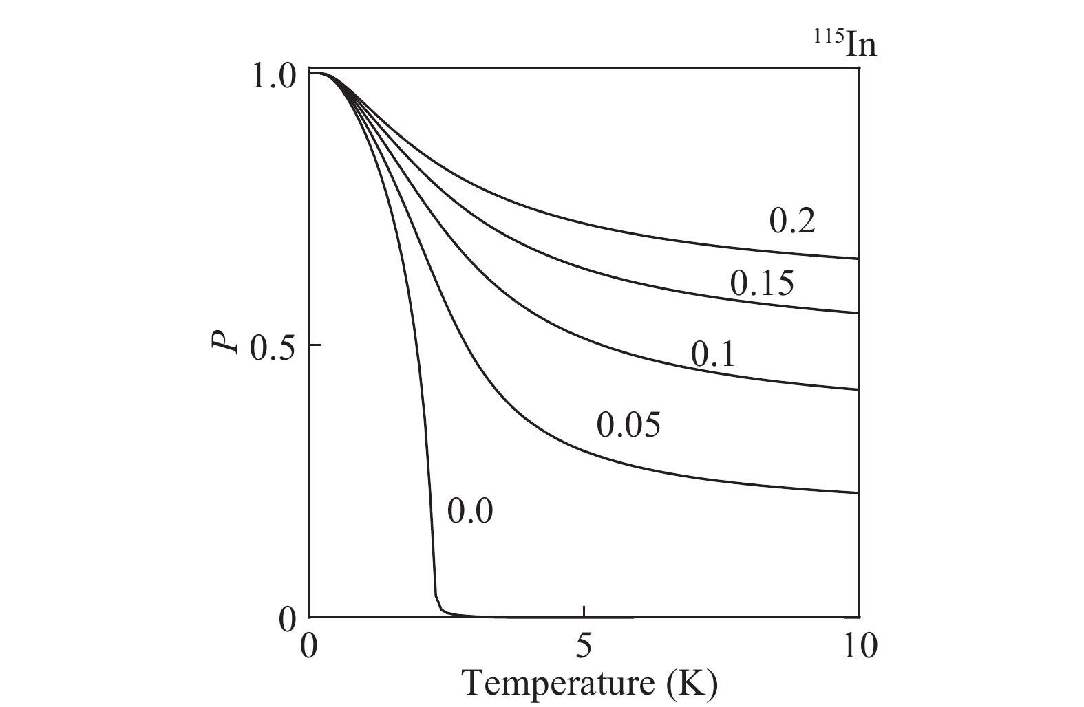
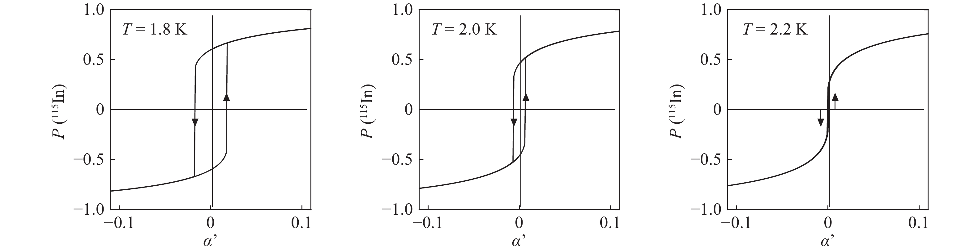
III–V semiconductors exhibit dynamic nuclear self-polarization (DYNASP) owing to the contact hyperfine interaction (HFI) between optically excited conduction electrons and lattice nuclei. In the self-polarization process at a low temperature, electron spin state and the nuclear polarization (magnetization) exchange a positive feedback, increasing energy splitting of the conduction electron states, thereby a large nuclear polarization. This phenomenon was theoretically predicted previously for conduction electrons excited linearly and elliptically polarized light. The polarization of the conduction electrons was represented by a parameterα in a formula for nuclear polarization (Eq. (9) in Ref. [1]); however, the effect of external magnetic fields on the nuclear polarization was not considered. Therefore, this study introduces this effect by further extending the previous studies. Herein, α′ represents the combination of the effects of elliptically polarized electrons and an external magnetic field, which is used in the equations presented in previous studies. When α′ = 0, a large nuclear polarization is obtained below critical temperature Tc, but no polarization occurs above Tc. When α′ > 0, the nuclear polarization is enhanced above Tc. Below Tc, the nuclear polarization follows a hysteresis curve when α′ is partially manipulated by adjusting the degree of the polarization of the exciting laser.
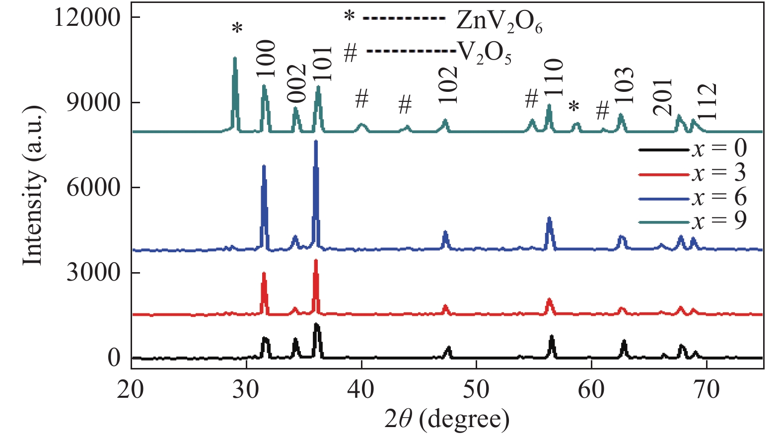
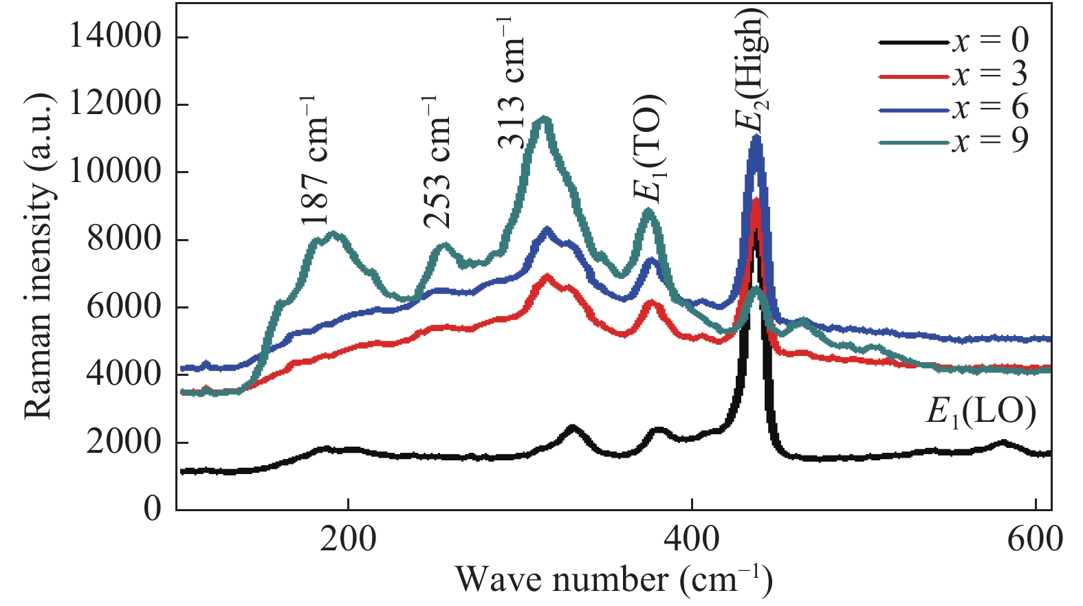
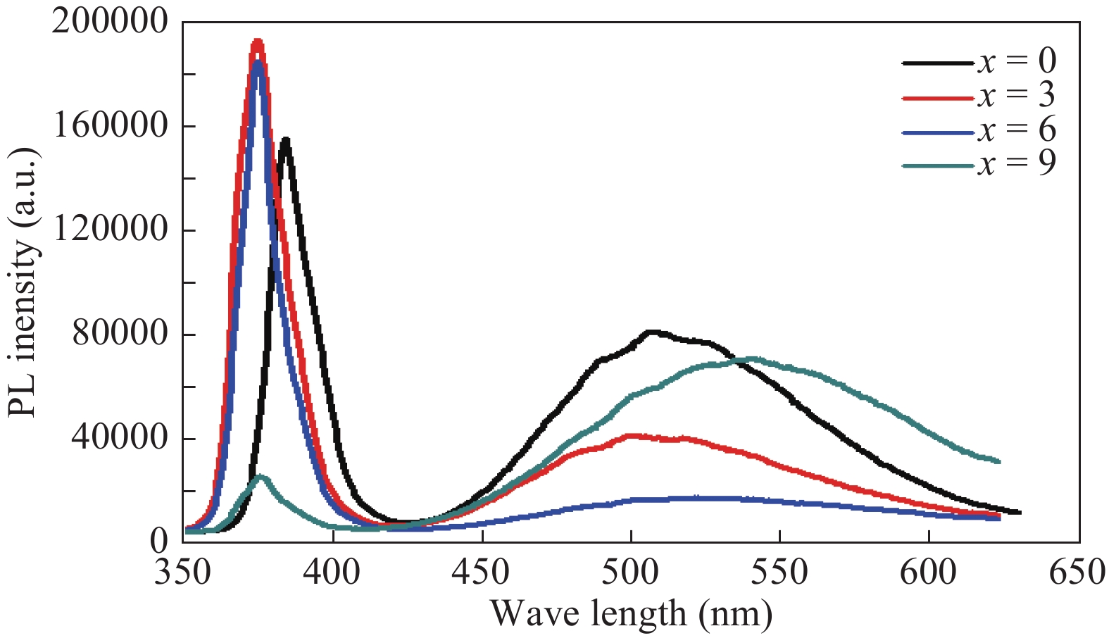
This paper demonstrates the structural, vibrational and photoluminescence characteristics of (ZnO)1−x(V2O5)x (x = 0, 3, 6 and 9 mol%) composites semiconductor synthesized by using the solid state reaction method. X-ray diffraction (XRD) studies show that (ZnO)1−x(V2O5)x composites have the poly crystalline wurtzite structure of hexagonal ZnO. It is found from the XRD results that the lattice constants and the crystallite size increase while the dislocation density decreases with increase in doping concentration. The existence of E1 (TO) and E2 (high) Raman modes show that the ZnO still preserve wurtzite structure after doping vanadium oxide, which is in agreement with XRD results. Room temperature photoluminescence (PL) exhibit near band edge and broad deep level emission while indicating the suppression of deep level emission with the incorporation of V2O5 up to a certain concentration (x < 9). Moreover, the optical band gap increase with doping, which is accompanied by the blue shift of the NBE emission.
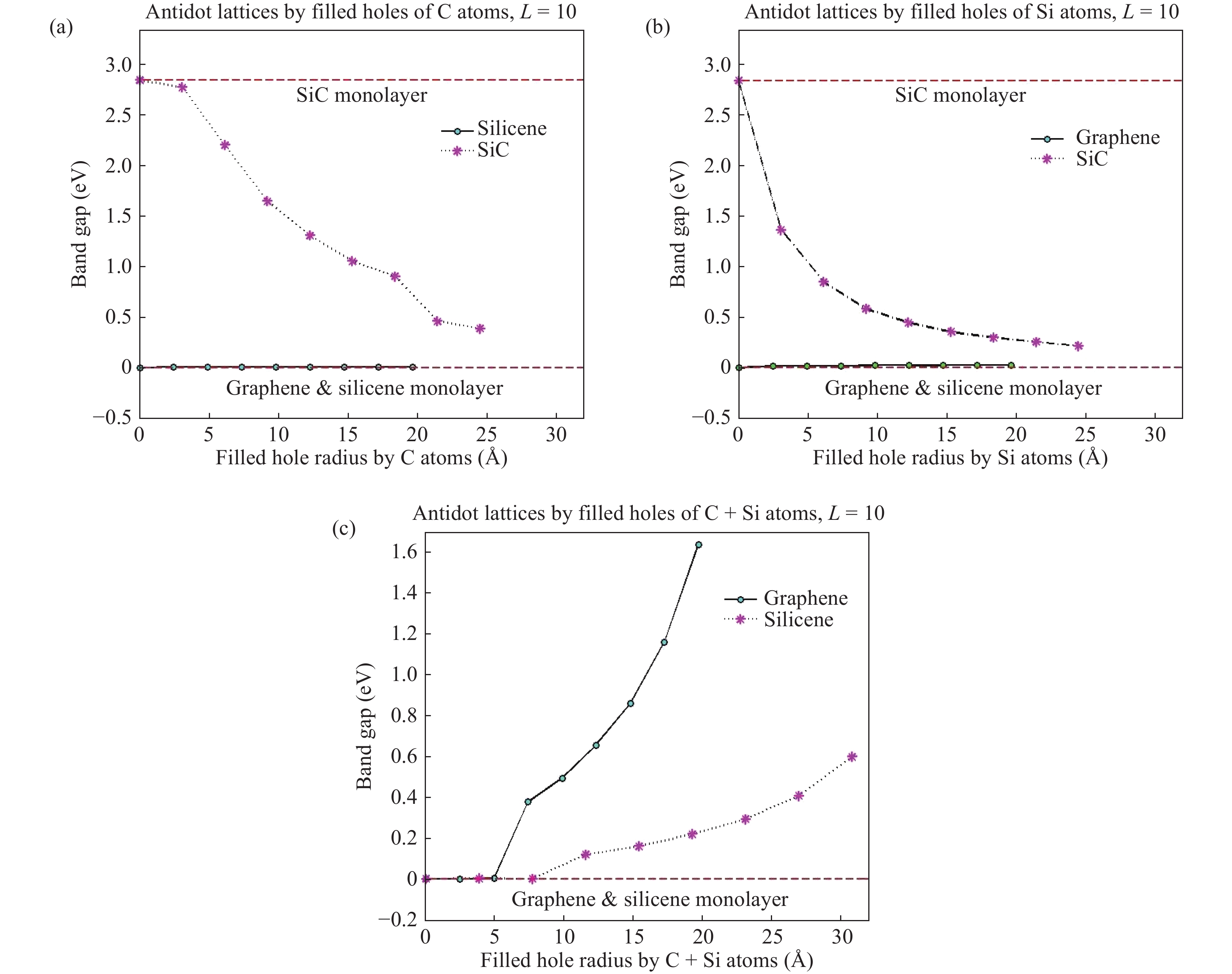
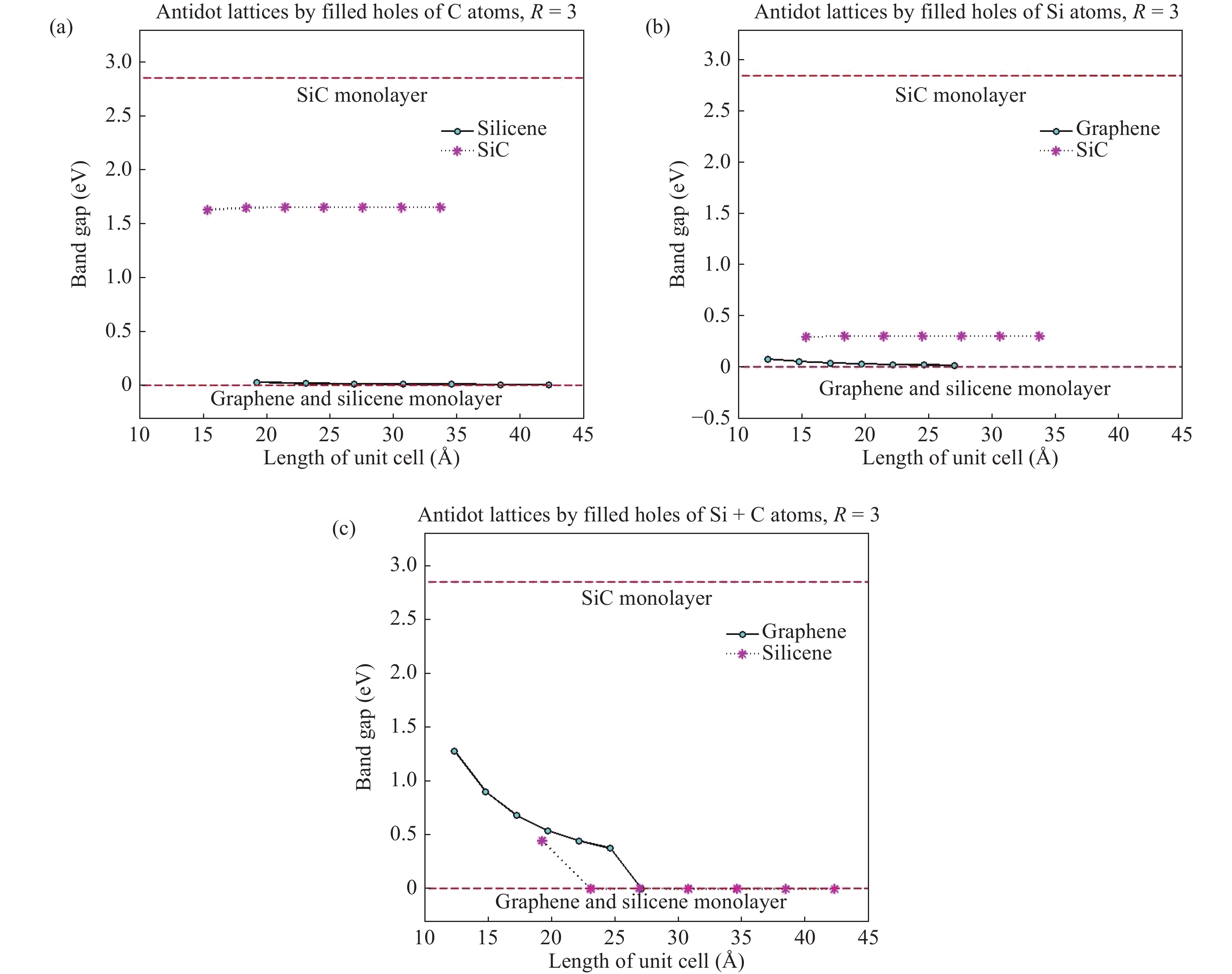
We have developed a

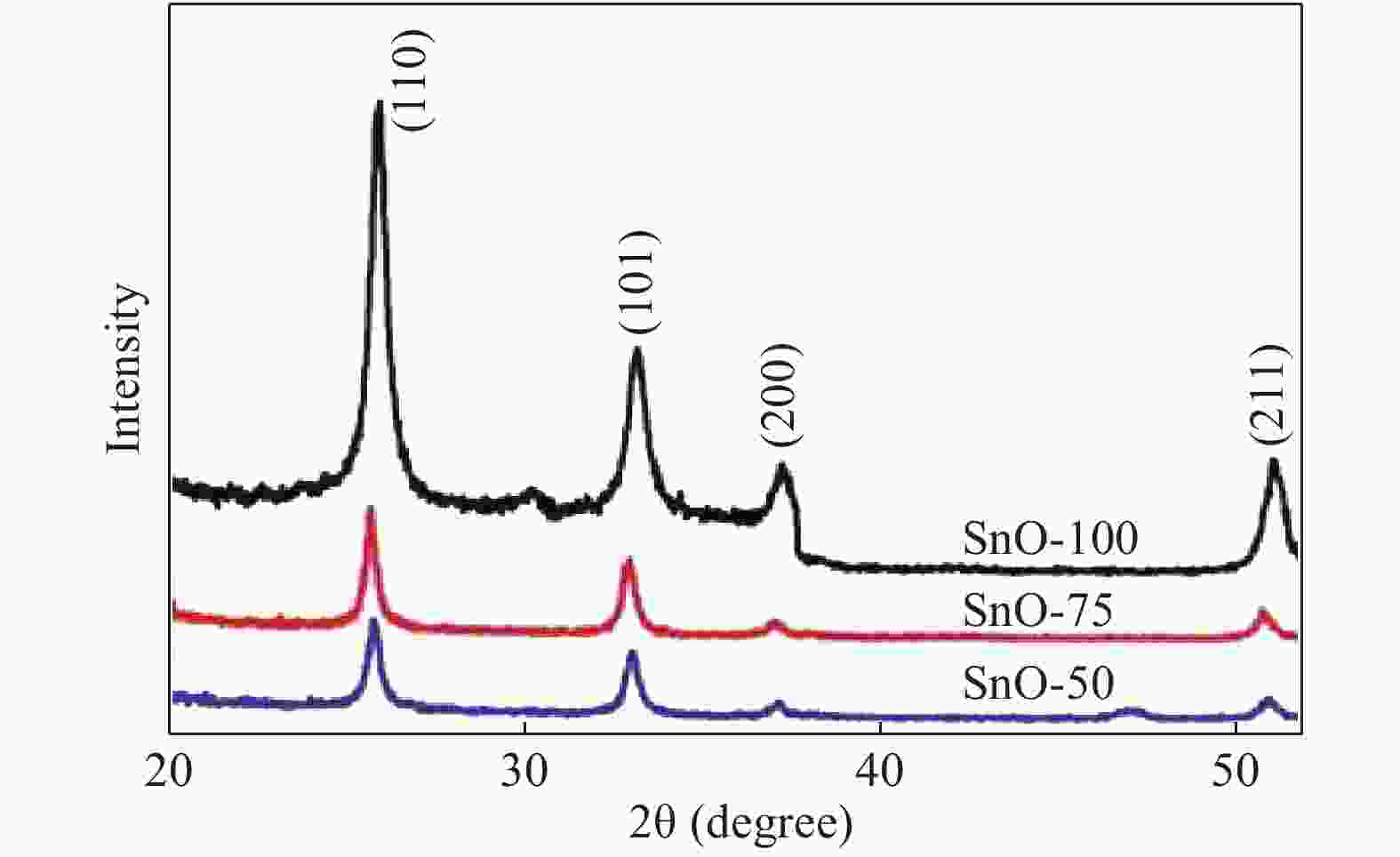
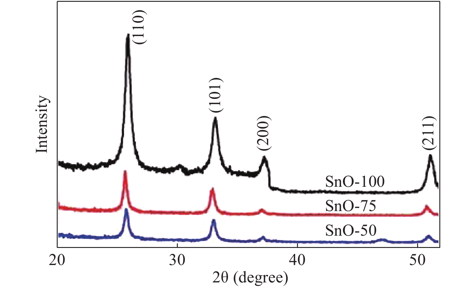
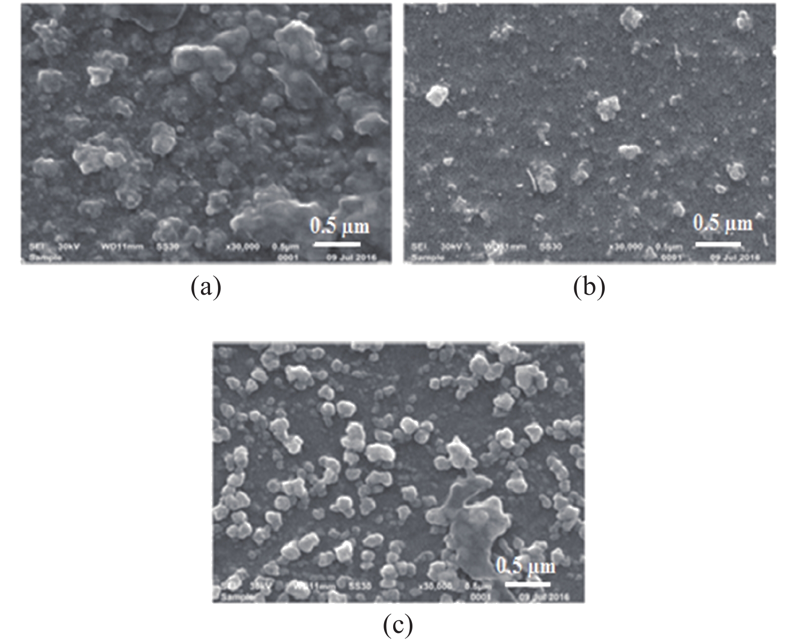
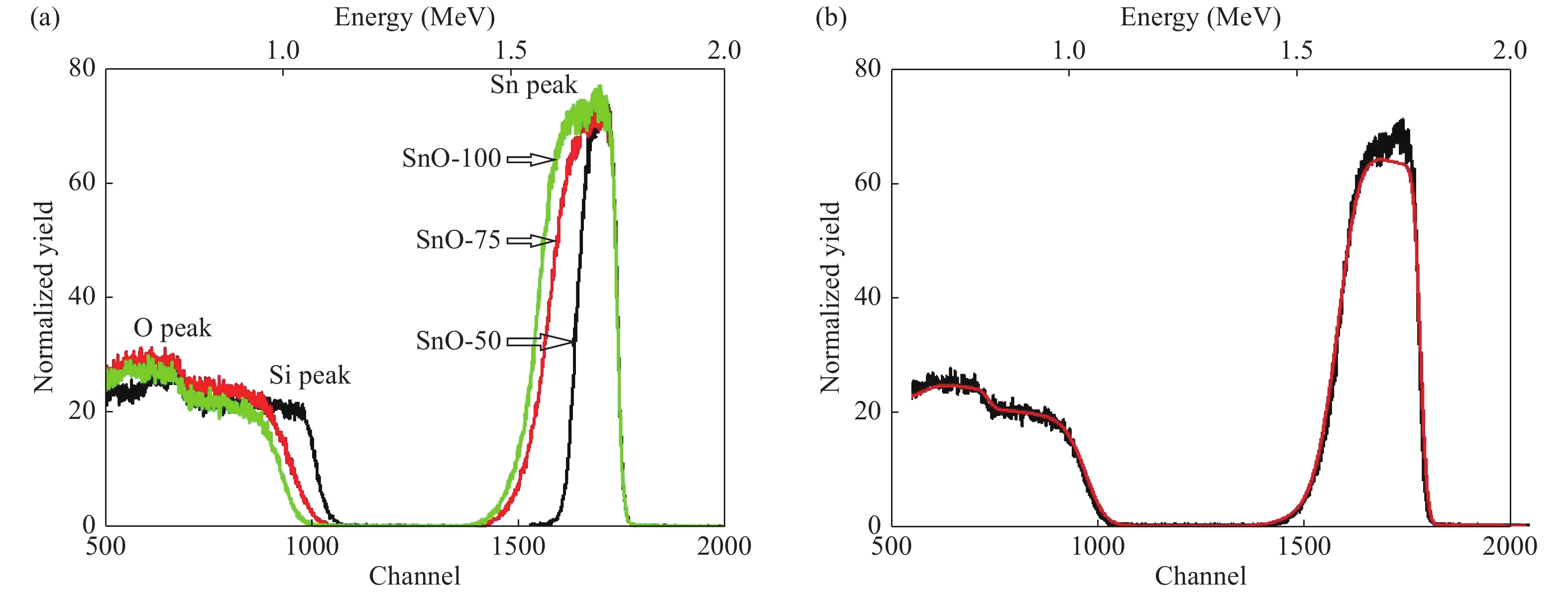
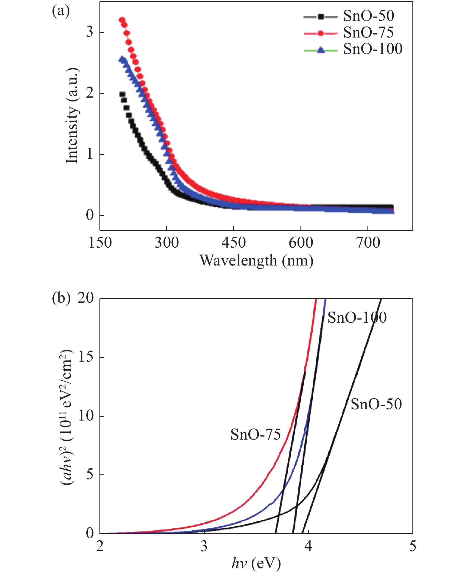
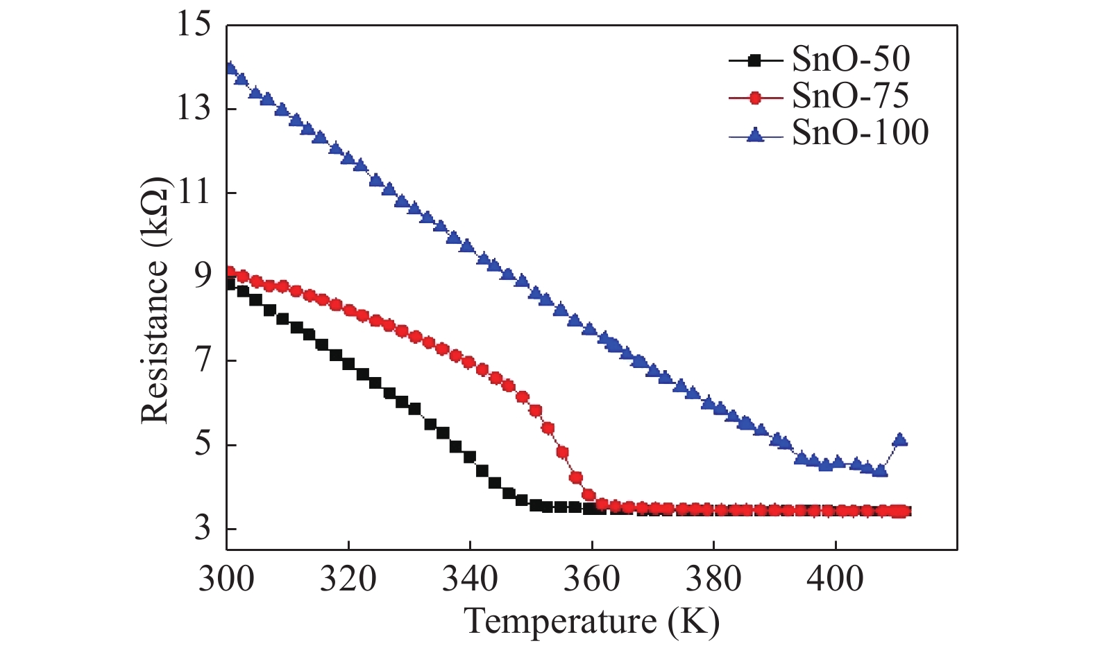
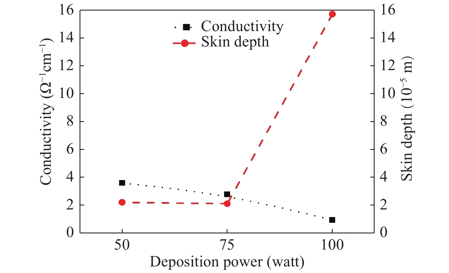
The role of deposition rate in the structural, optical and electrical properties of SnO2 thin films deposited by electron beam evaporation method is investigated by varying the deposition powers viz. 50, 75, and 100 W. The structural characterization of the films is done by X-ray diffraction (XRD) technique. The surface morphology of the films is studied by scanning electron microscopy (SEM). Rutherford back scattering (RBS) measurements revealed the thickness of the films ranging from 200 nm to 400 and also a change in the concentration of oxygen vacancies which is found to be the maximum in the film deposited at the lowest deposition rate. Optical absorption spectrum is recorded using the UV–V is spectroscopy and the films are found to be transparent in nature. A shift in the absorption edge is observed and is attributed to a different level of allowed energy states in conduction band minimum. The Hall effect and electrical measurements show a variation in the carrier concentrations, mobility and resistivity of the films. In order to explore a better compromise in electrical and optical properties for transparent electrode applications, skin depths calculations are also done to find the optimized values of carrier concentration and mobility.
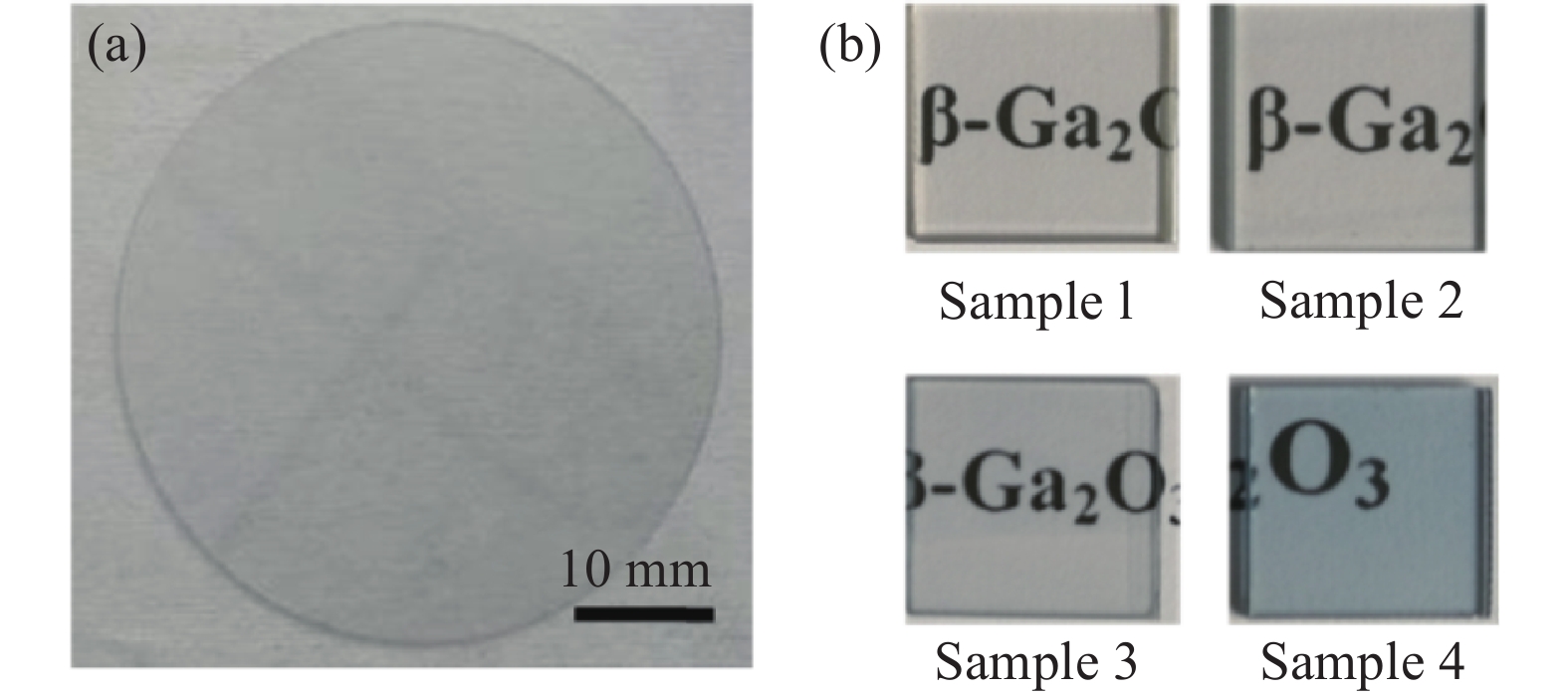
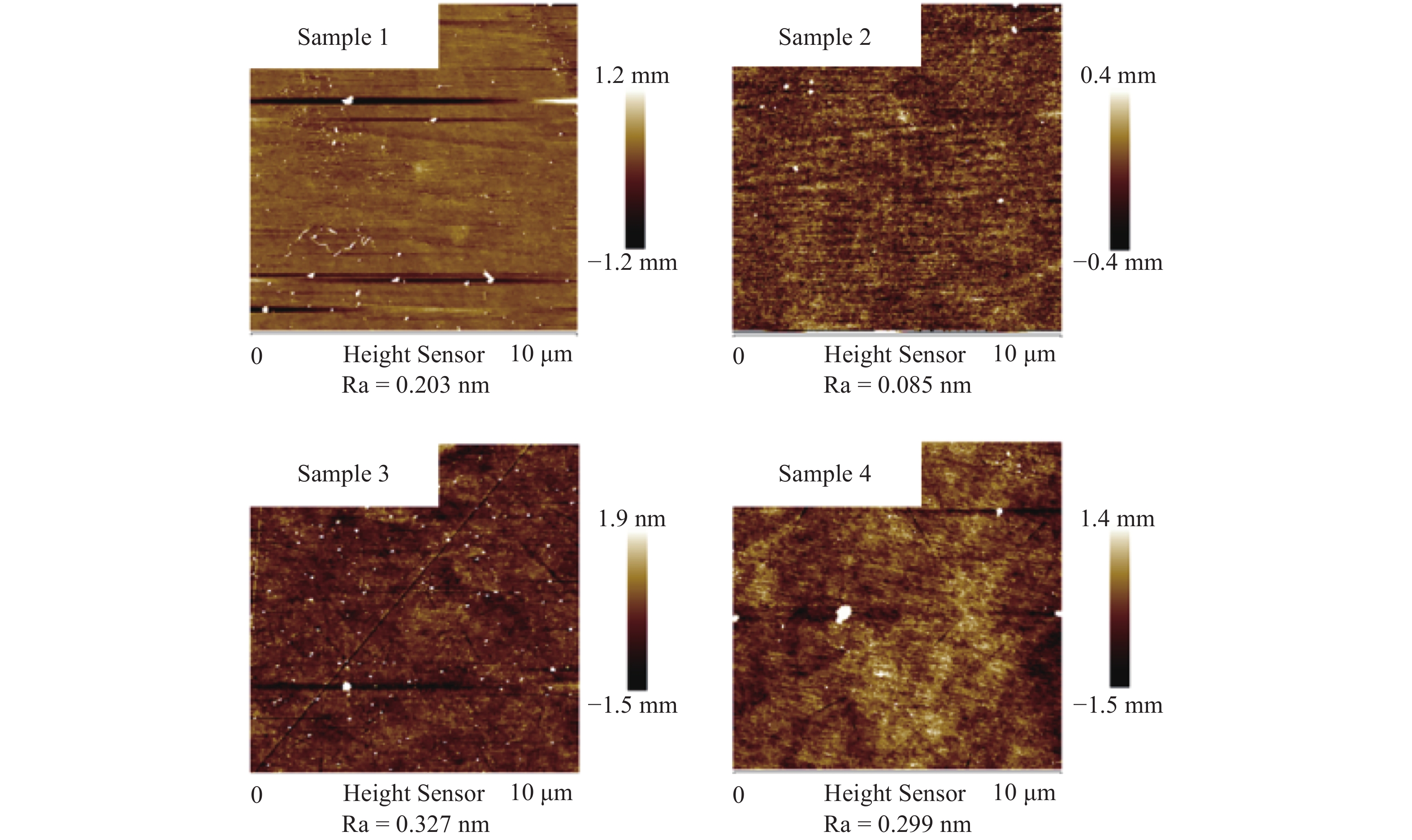
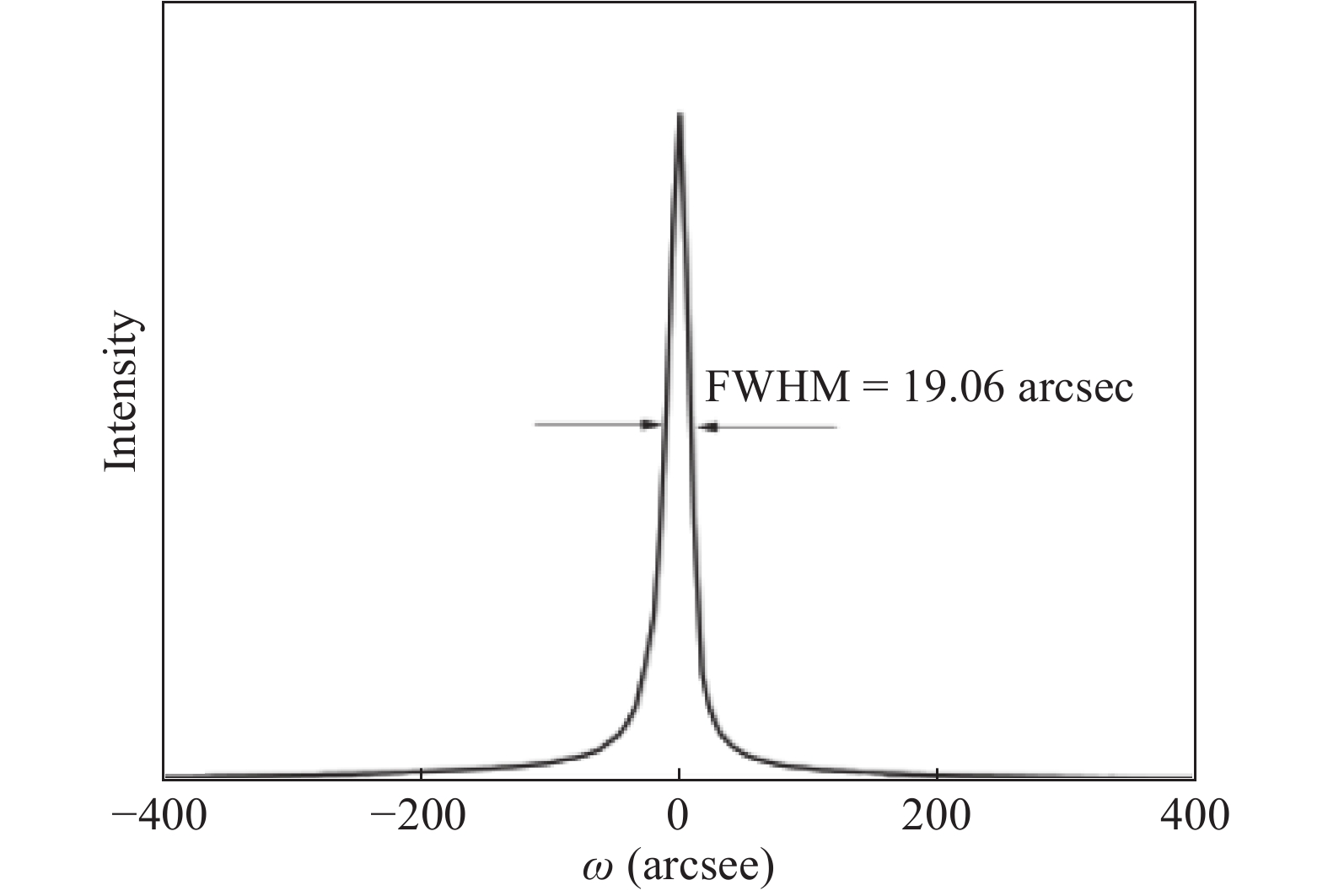
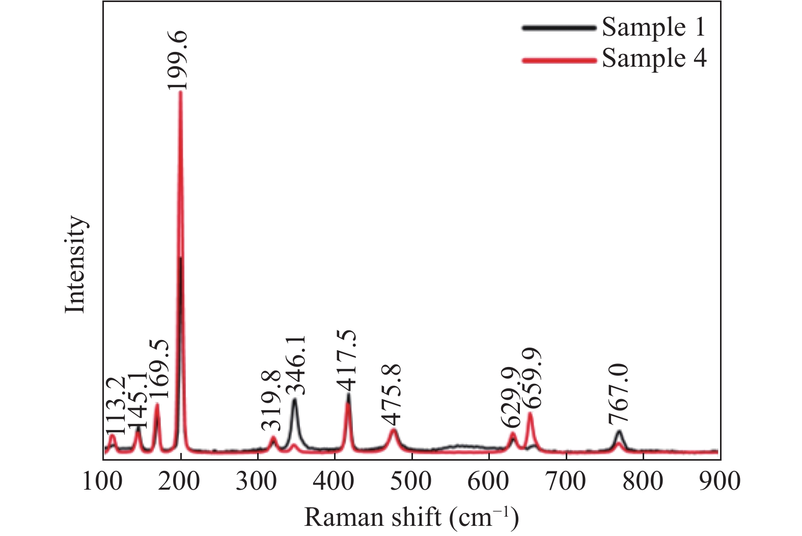
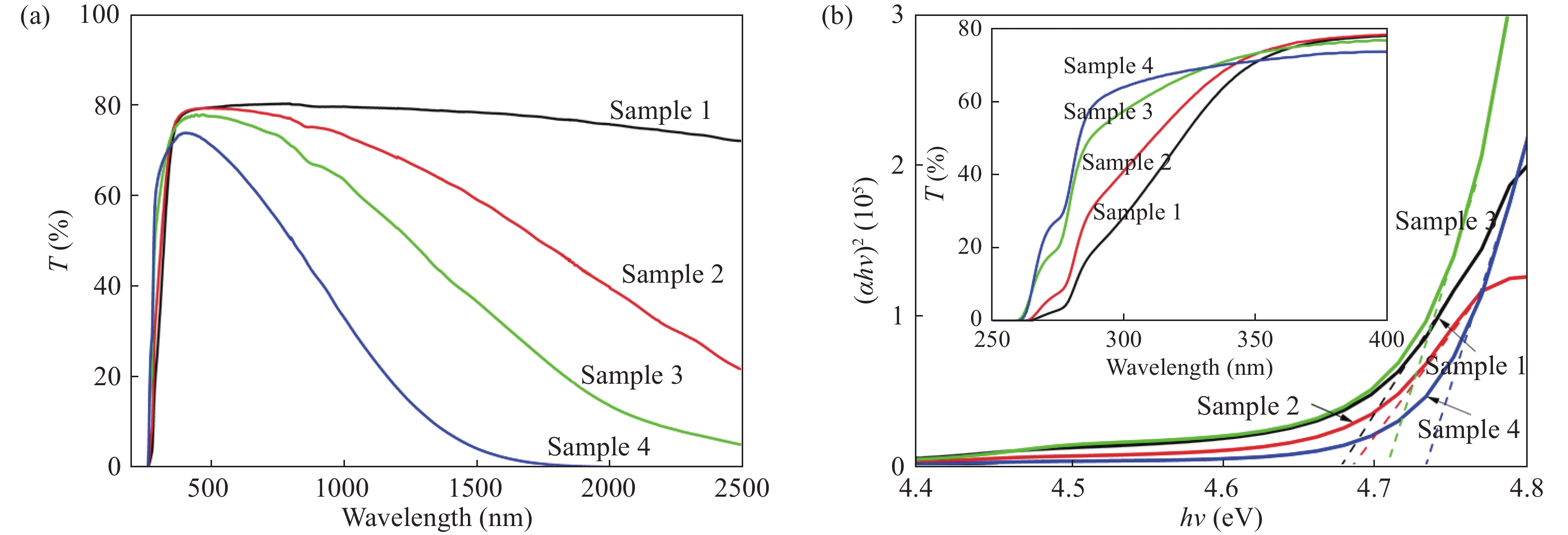
β-Ga2O3 is an ultra-wide band-gap semiconductor with promising applications in UV optical detectors, Schottky barrier diodes, field-effect transistors and substrates for light-emitting diodes. However, the preparation of large β-Ga2O3 crystals is undeveloped and many properties of this material have not been discovered yet. In this work, 2-inch β-Ga2O3 single crystals were grown by using an edge-defined film-fed growth method. The high quality of the crystal has been proved by high-resolution X-ray diffraction with 19.06 arcsec of the full width at half maximum. The electrical properties and optical properties of both the unintentionally doped and Si-doped β-Ga2O3 crystals were investigated systematically.
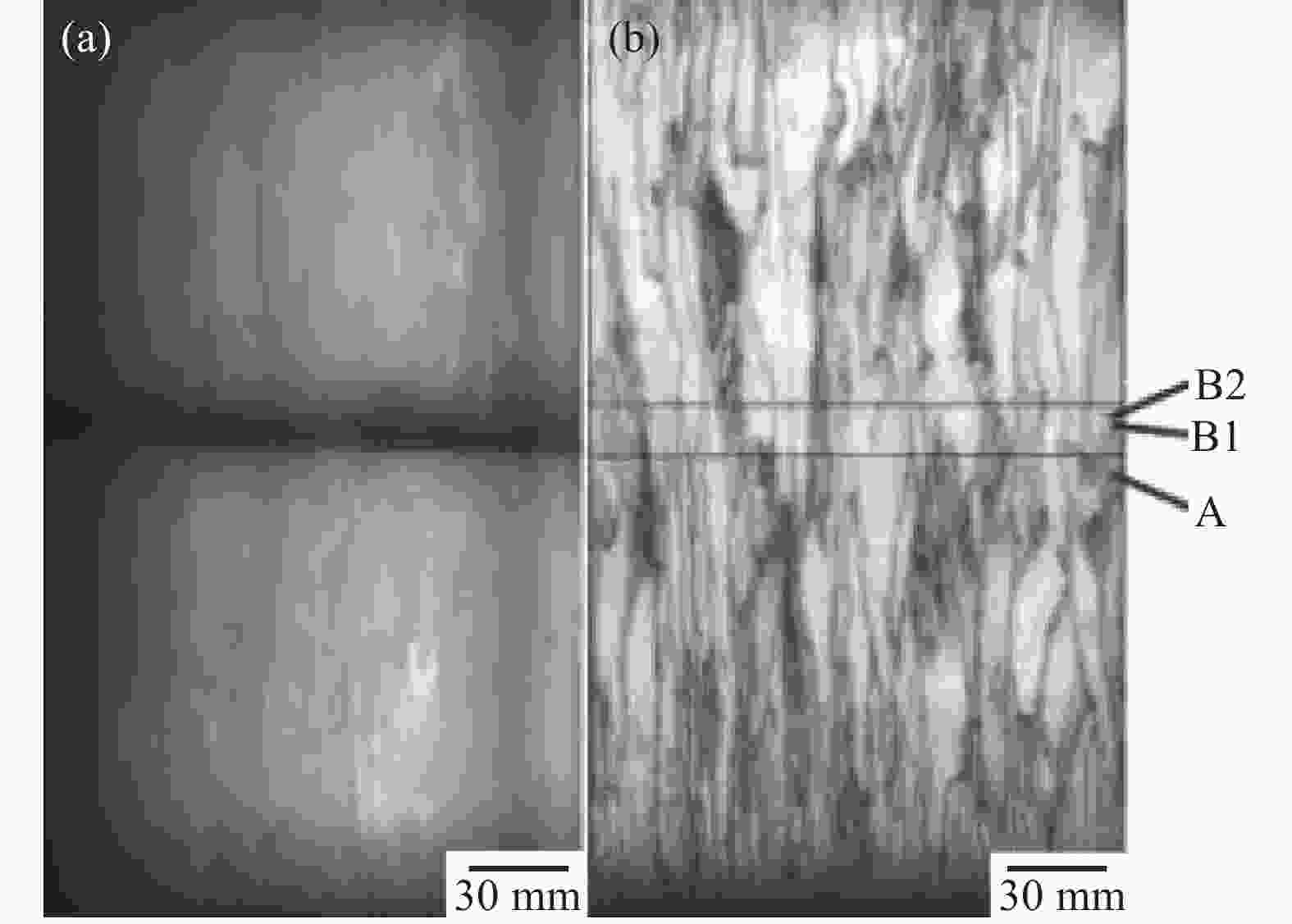
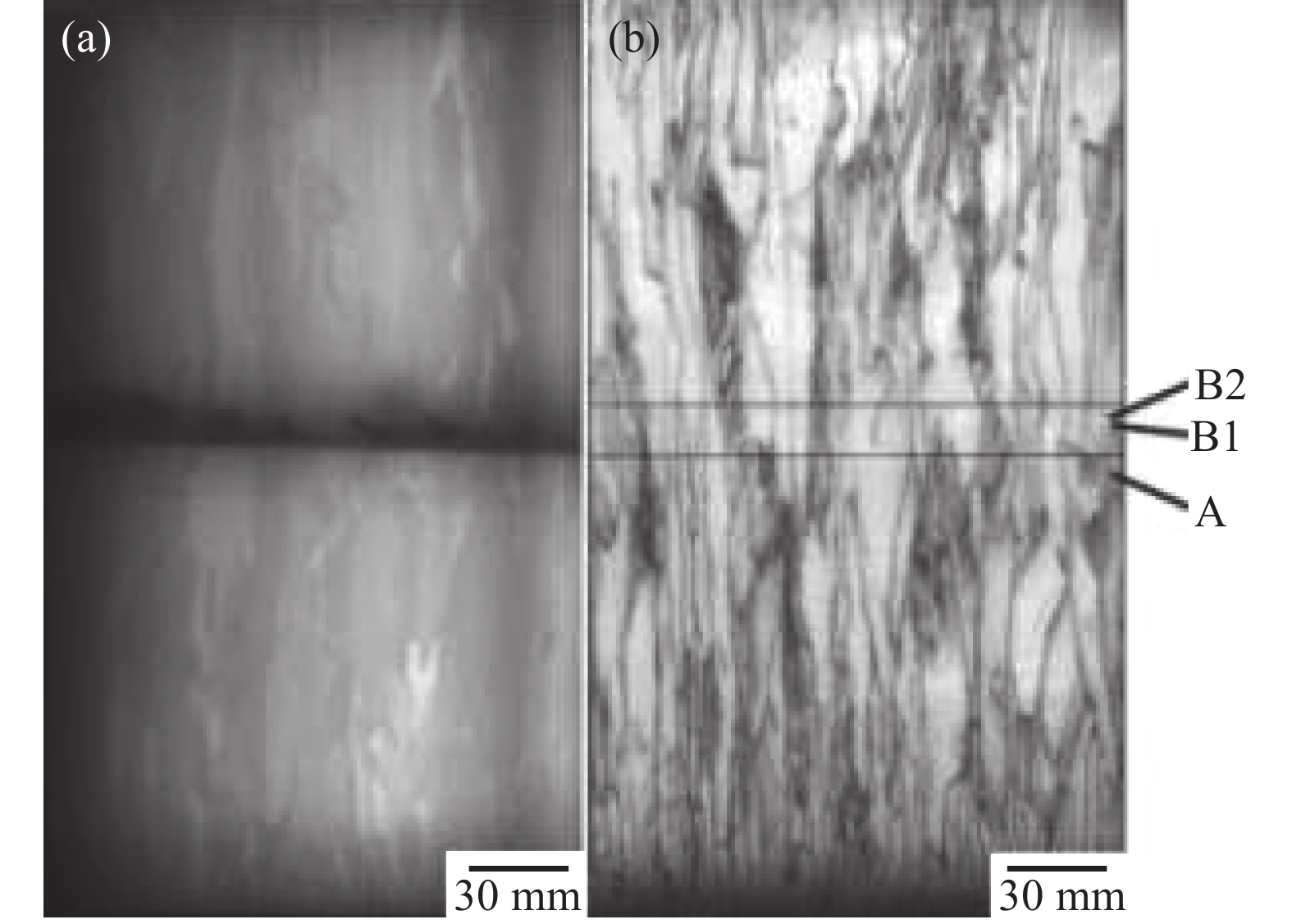
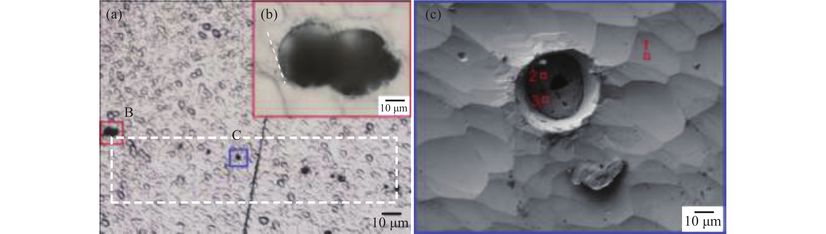
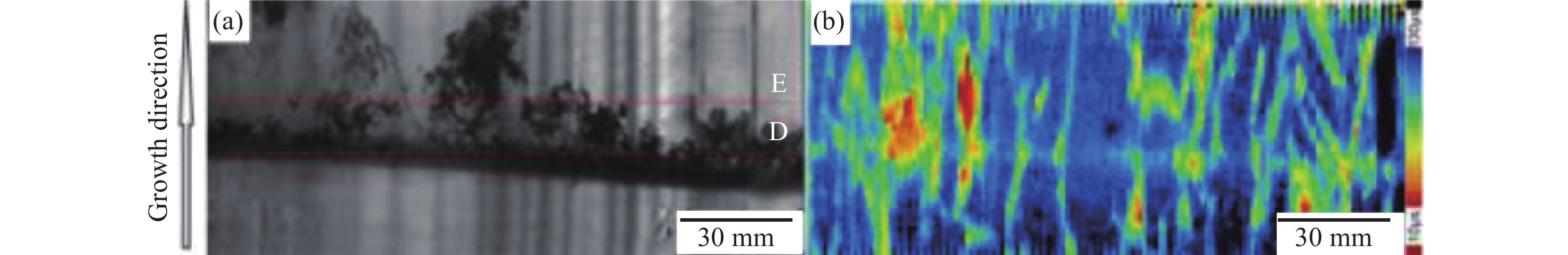
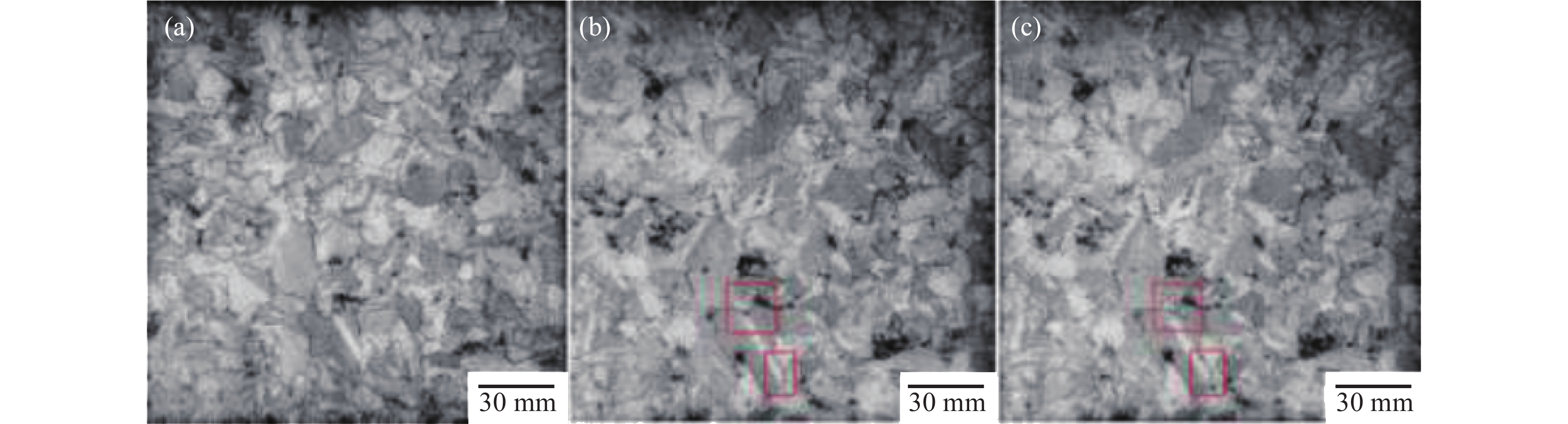
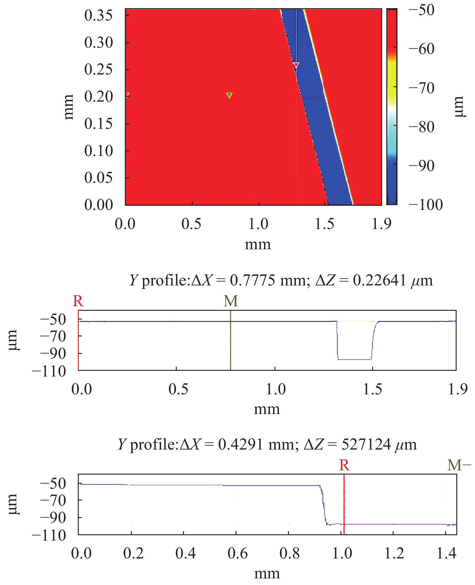
We characterized strip-like shadows in cast multicrystalline silicon (mc-Si) ingots. Blocks and wafers were analyzed using scanning infrared microscopy, photoluminescence spectroscopy, laser scanning confocal microscopy, field-emission scanning electron microscopy, X-ray energy-dispersive spectrometry, and microwave photoconductivity decay technique. The effect on solar cell performance is discussed. The results show that the non-microcrystalline shadow region in Si ingots consists of precipitates of Fe, O, and C. The size of these Fe–O–C precipitates found at the shadow region is ~25 μm. Fe–O–C impurities can slightly reduce the minority carrier lifetime of the wafers while severely decrease in shunt resistance, leading to the increase in reverse current of the solar cells and degradation in cell efficiency.
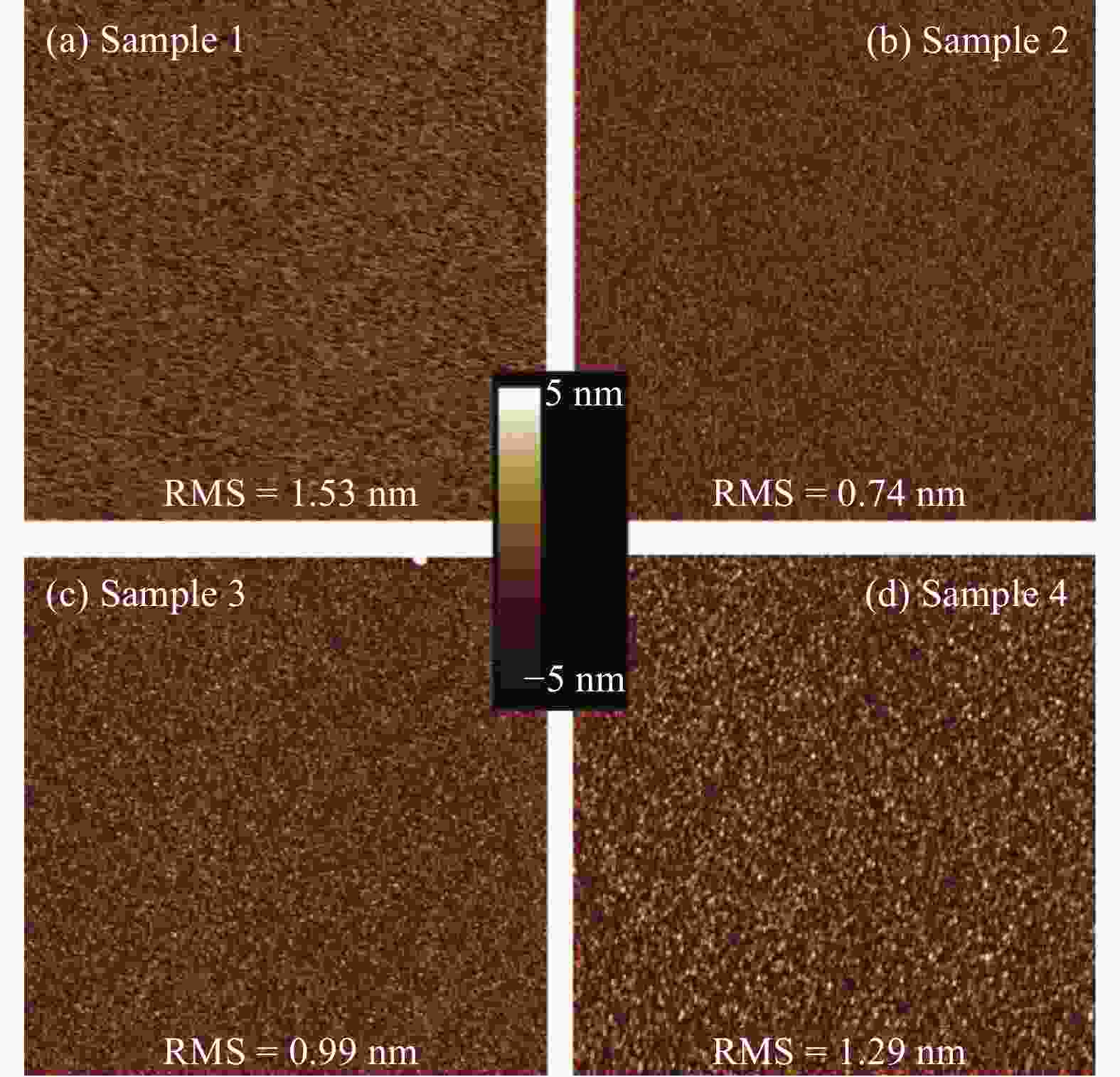
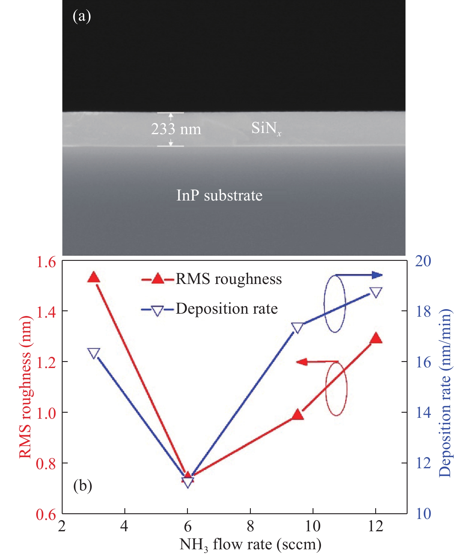
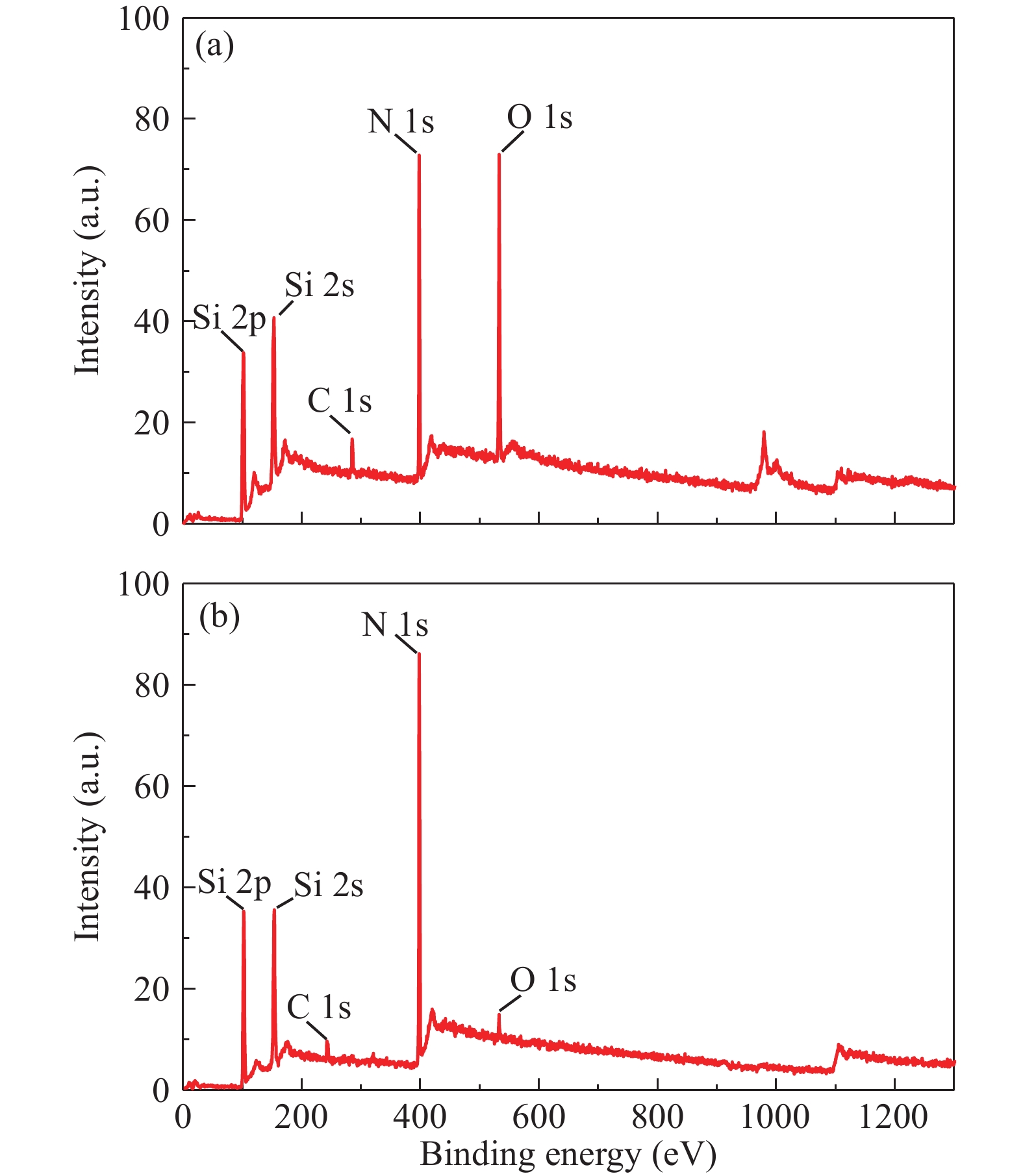
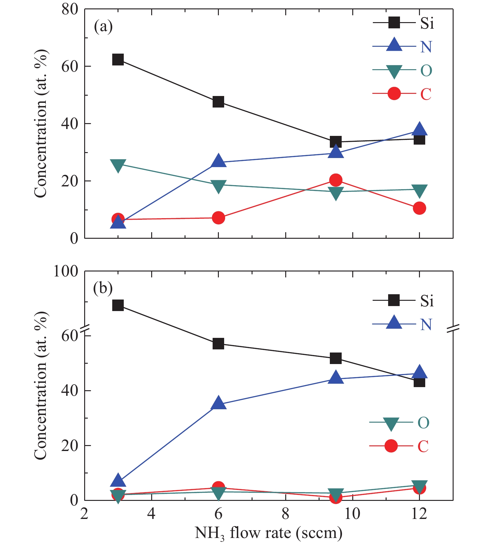
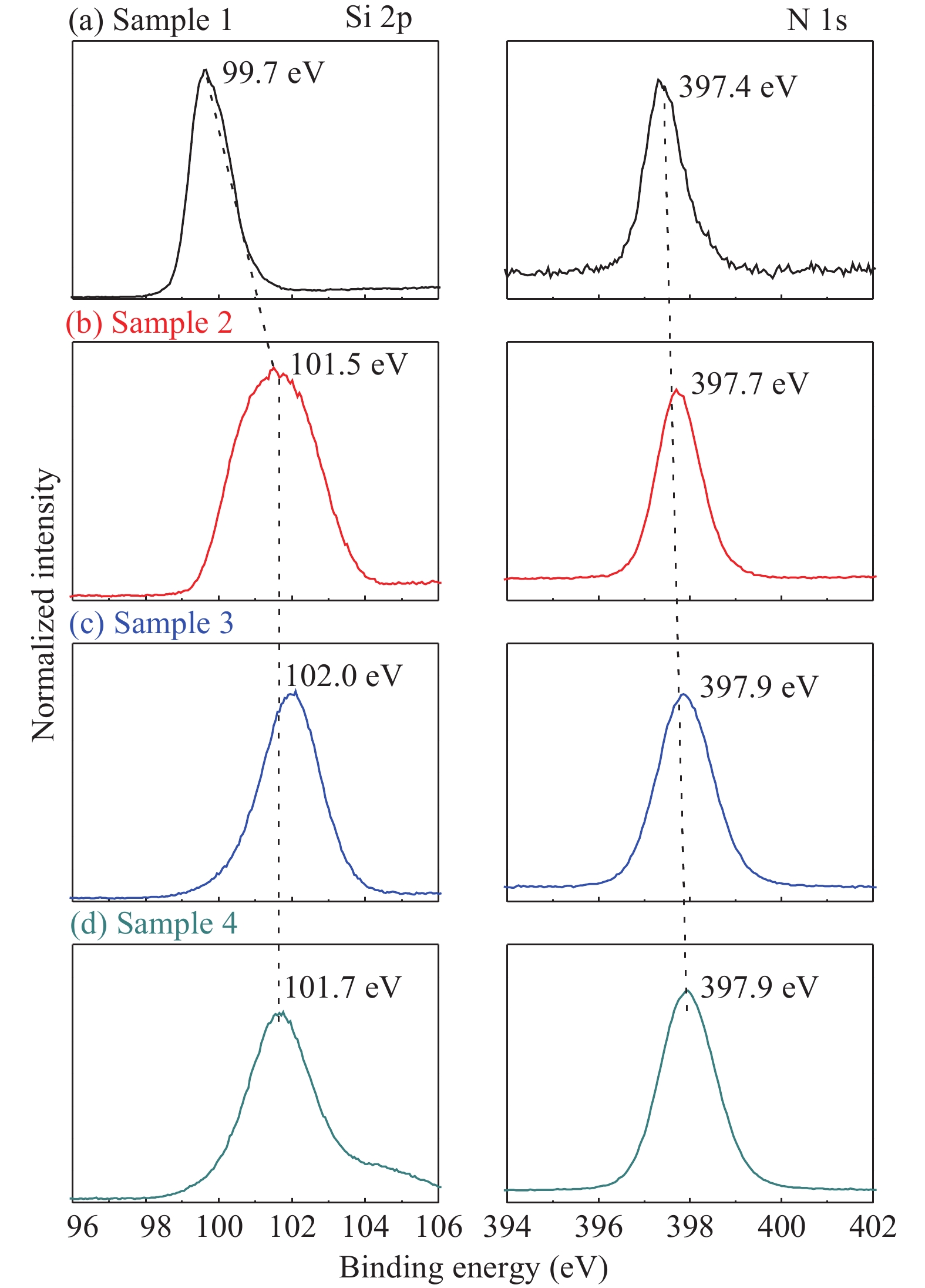
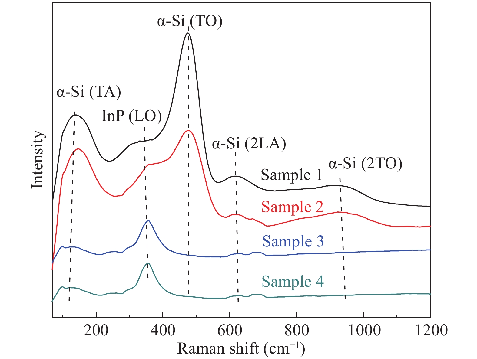
The surface and optical properties of silicon nitride samples with different compositions were investigated. The samples were deposited on InP by inductively coupled plasma chemical vapor deposition using different NH3 flow rates. Atomic force microscopy measurements show that the surface roughness is increased for the samples with both low and high NH3 flow rates. By optimization, when the NH3 flow rate is 6 sccm, a smooth surface with RMS roughness of 0.74 nm over a 5 × 5 μm2 area has been achieved. X-ray photoelectron spectroscopy measurements reveal the Si/N ratio of the samples as a function of NH3 flow rate. It is found that amorphous silicon is dominant in the samples with low NH3 flow rates, which is also proved in Raman measurements. The bonding energies of the Si and N atoms have been extracted and analyzed. Results show that the bonding states of Si atoms transfer from Si0 to Si+4 as the NH3 flow rate increases.
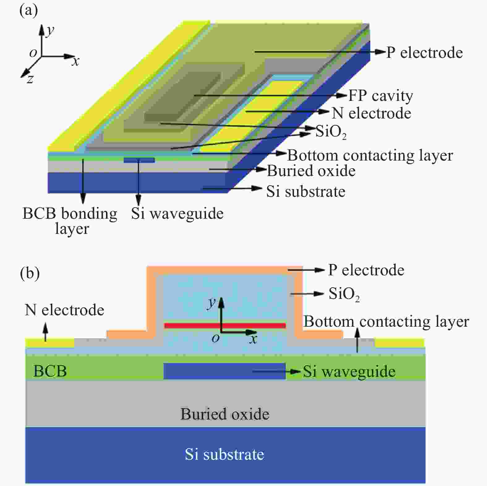
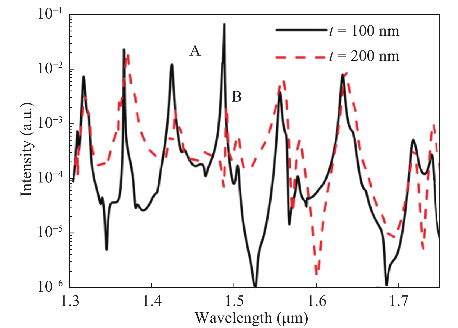
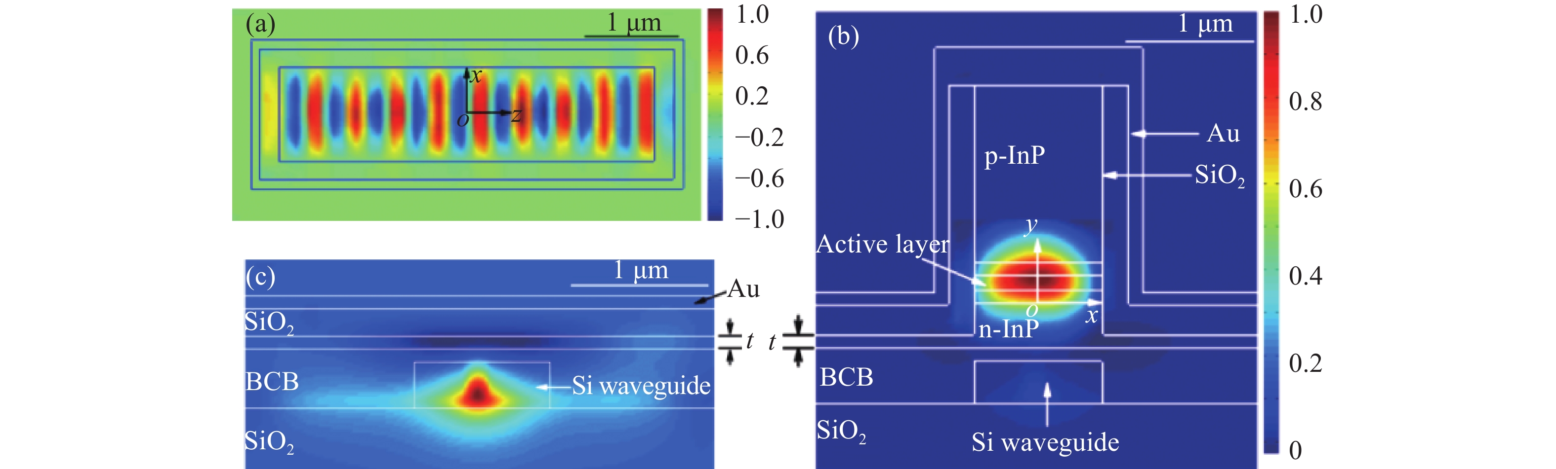
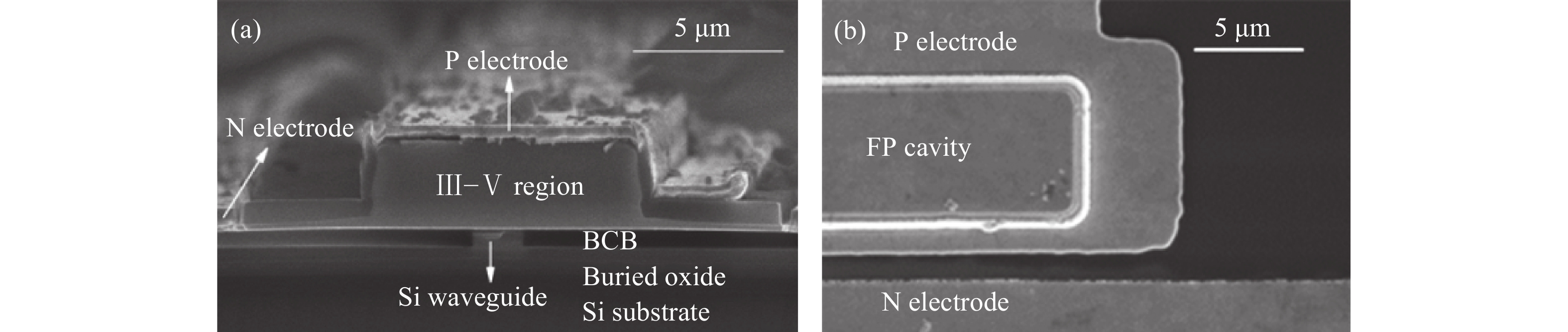
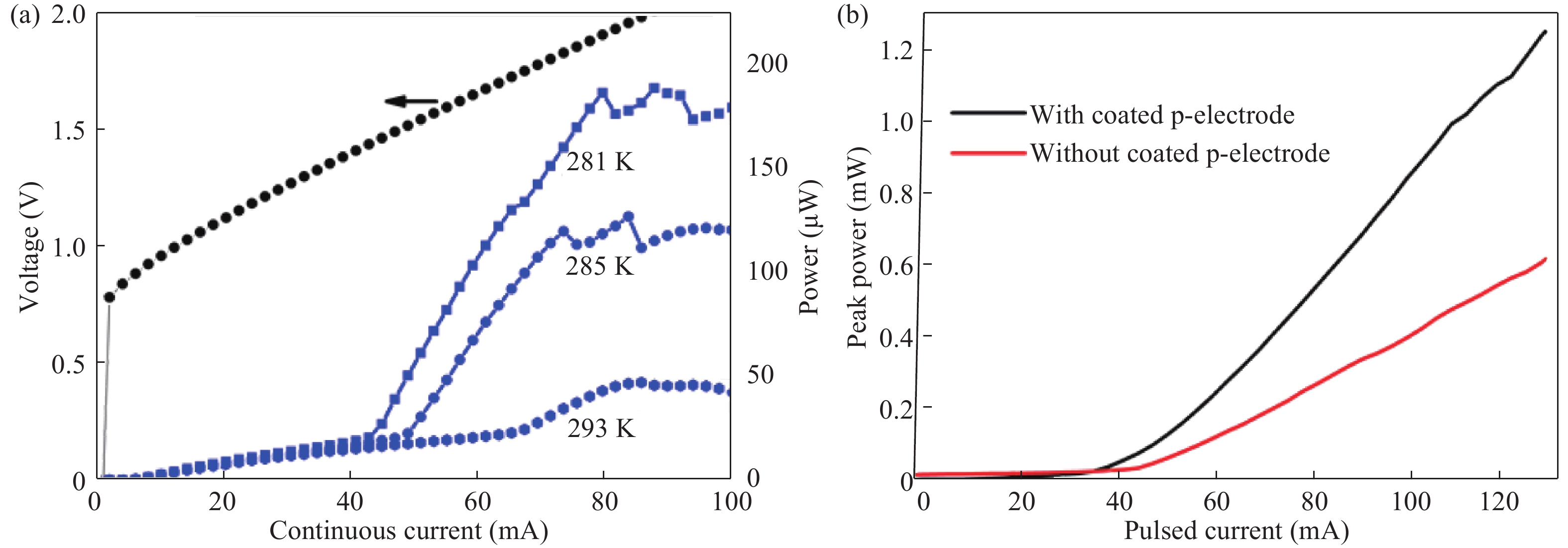
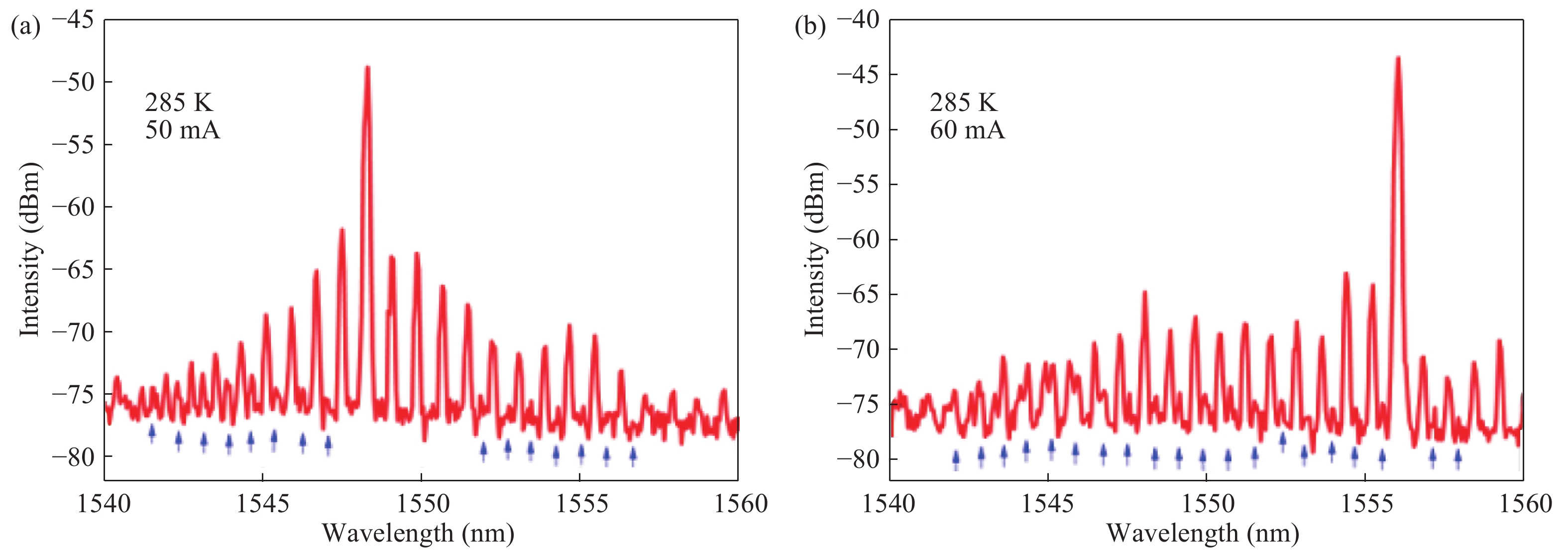
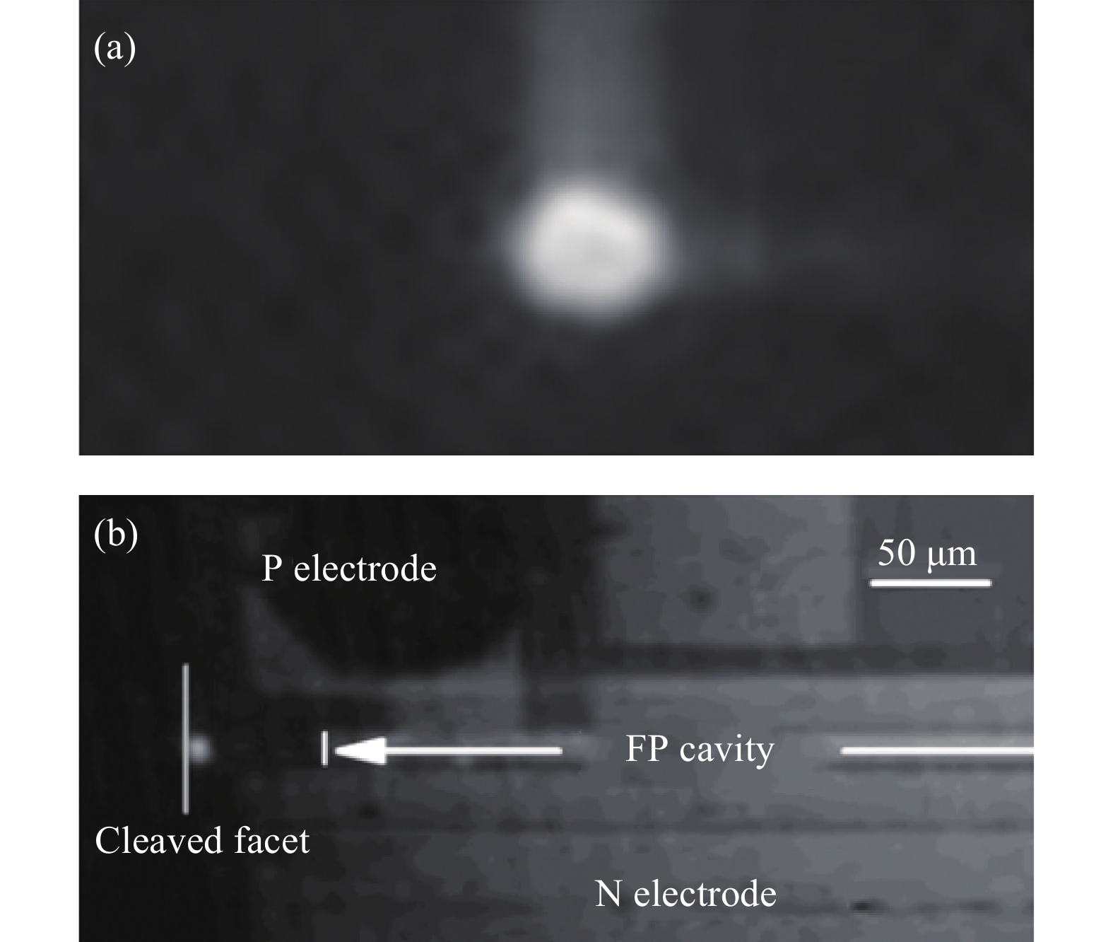
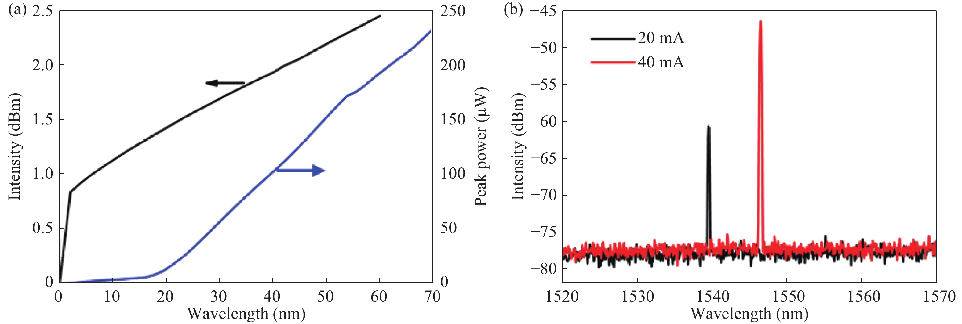
We have proposed and demonstrated hybrid AlGaInAs/Si Fabry–Pérot (FP) lasers, with the FP cavity facet covered by the p-electrode metal for enhancing mode confinement. Continuous-wave lasing is obtained at room temperature with a threshold current of 45 mA for the hybrid FP laser with a cavity length of 415 μm and a width of 7 μm. Near-field optical microscope images indicate an efficient output emission from the underneath evanescently-coupled silicon waveguide. Furthermore, single-mode lasing with a side-mode suppression-ratio of 29 dB and a threshold current of 16 mA is realized for the 150 μm-long hybrid FP laser.

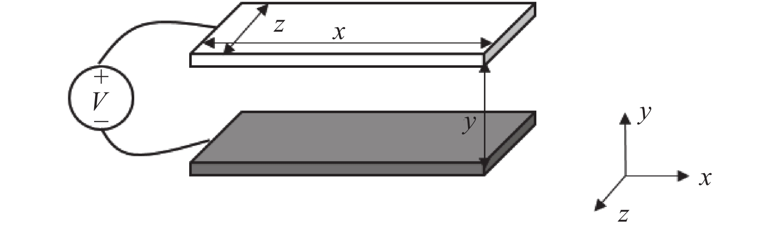
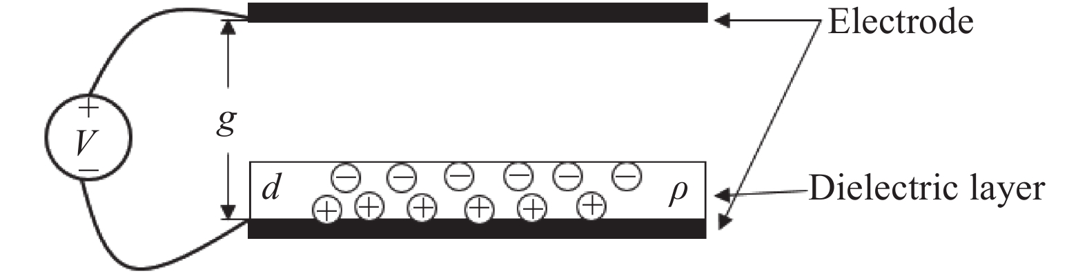
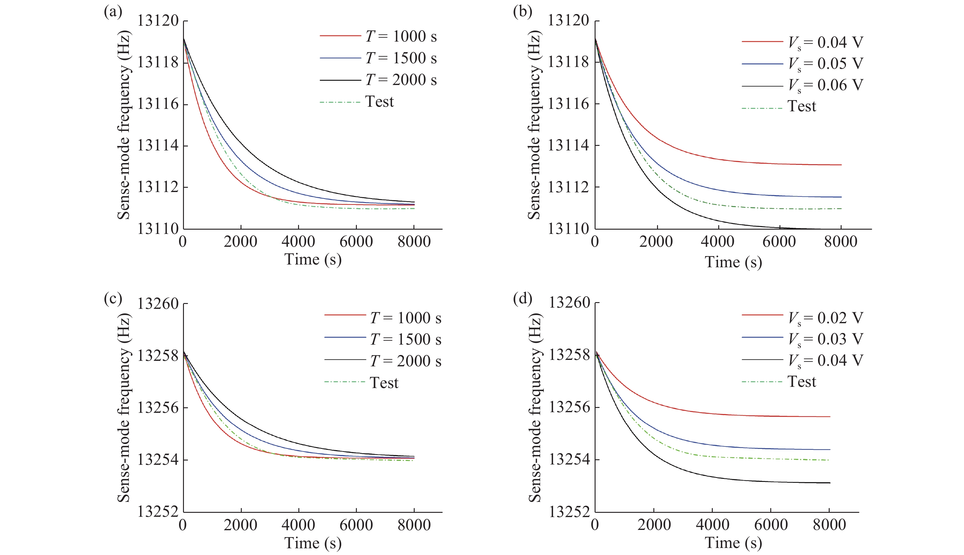
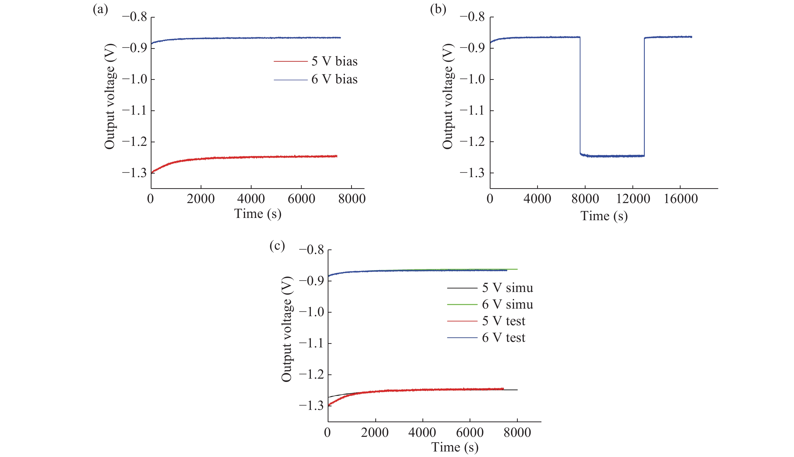
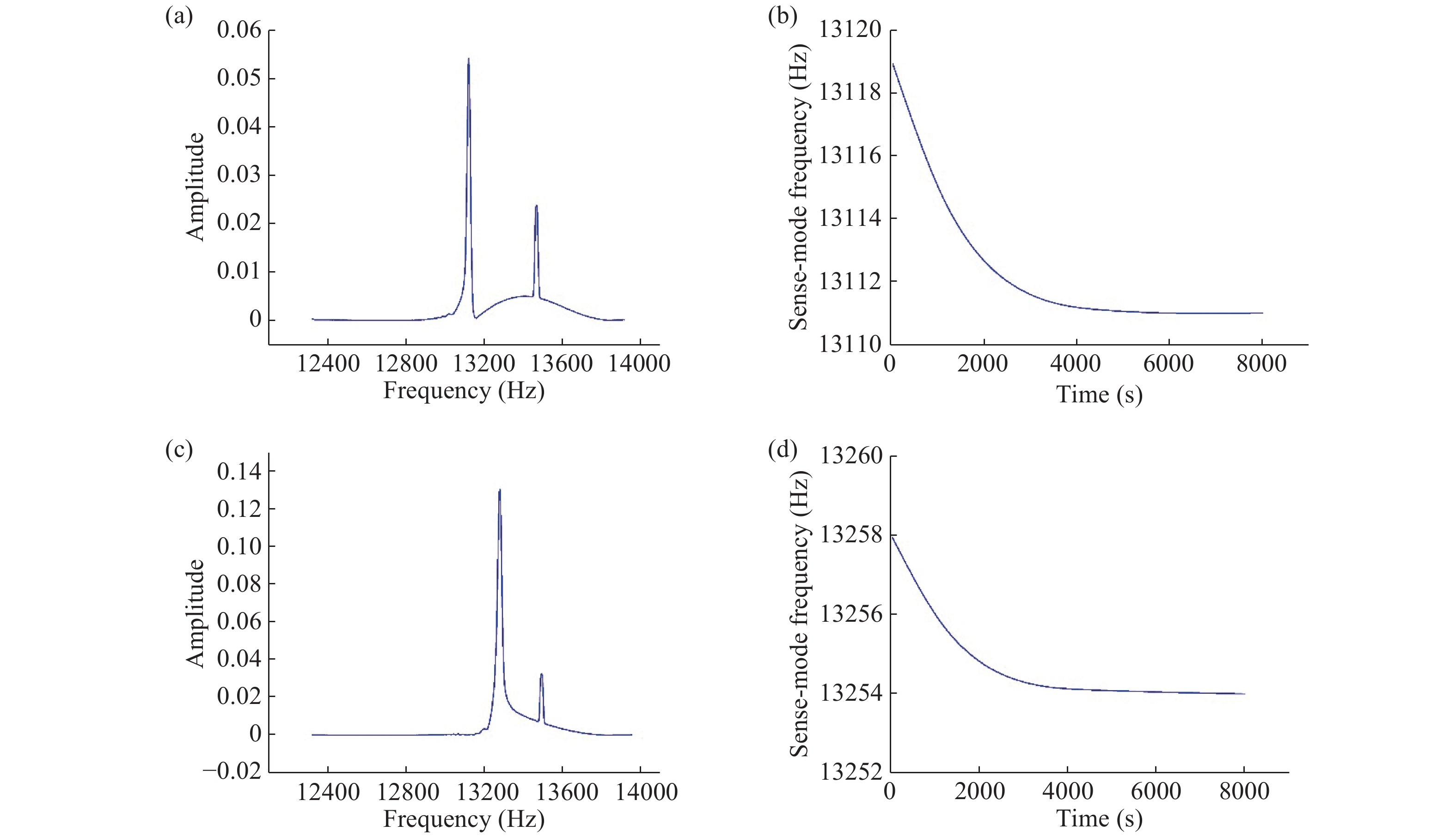
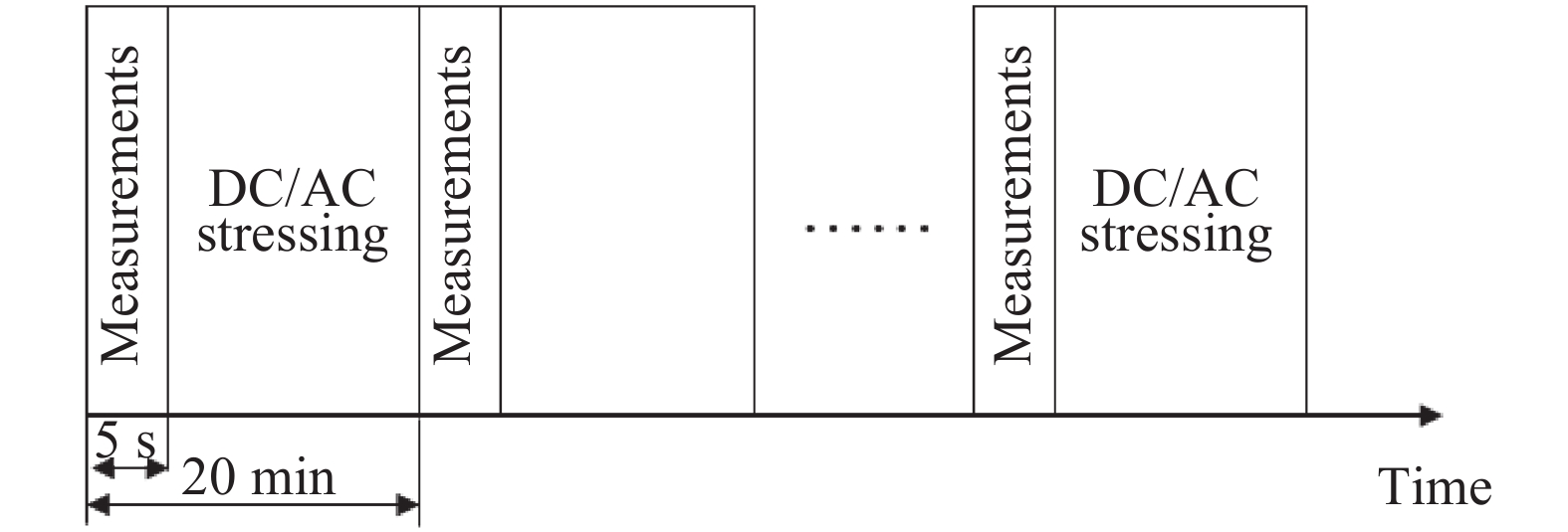
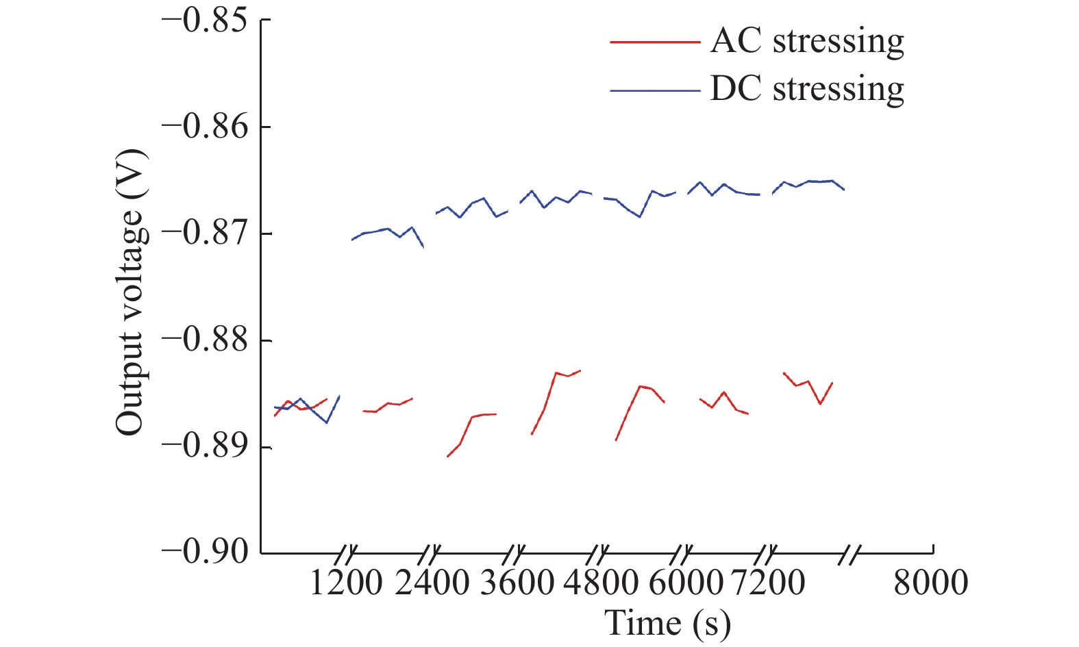
Output voltage drifting was observed in MEMS gyroscopes. Other than the quadrature error, frequency mismatch and quality factor, the dielectric parasitic charge was thought to be a major determinant. We studied the mechanism and variation of the parasitic charge in the MEMS gyroscopes, and analyzed the effect of the parasitic charge on the output stability. This phenomenon was extremely obvious in the Pyrex encapsulated MEMS gyroscopes. Due to the DC voltage required for the electrostatic actuation, the parasitic charge in the dielectric layer would accumulate and induce a residual voltage. This voltage had an impact on the resonant frequency of the gyroscopes, so as to affect the output stability. The theoretical studies were also confirmed by our experimental results. It was shown that the parasitic charge was harmful to the output stability of MEMS gyroscopes.
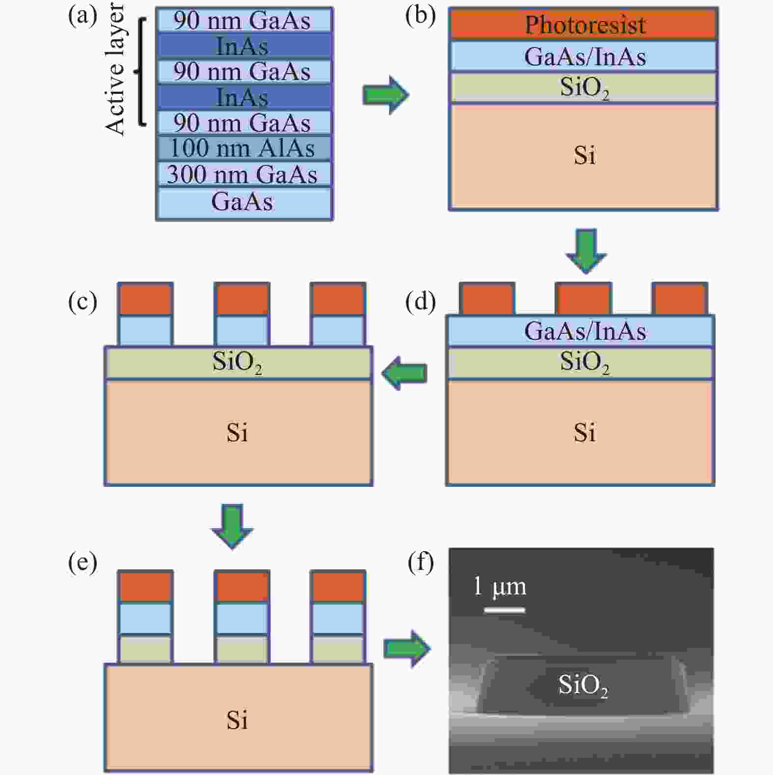
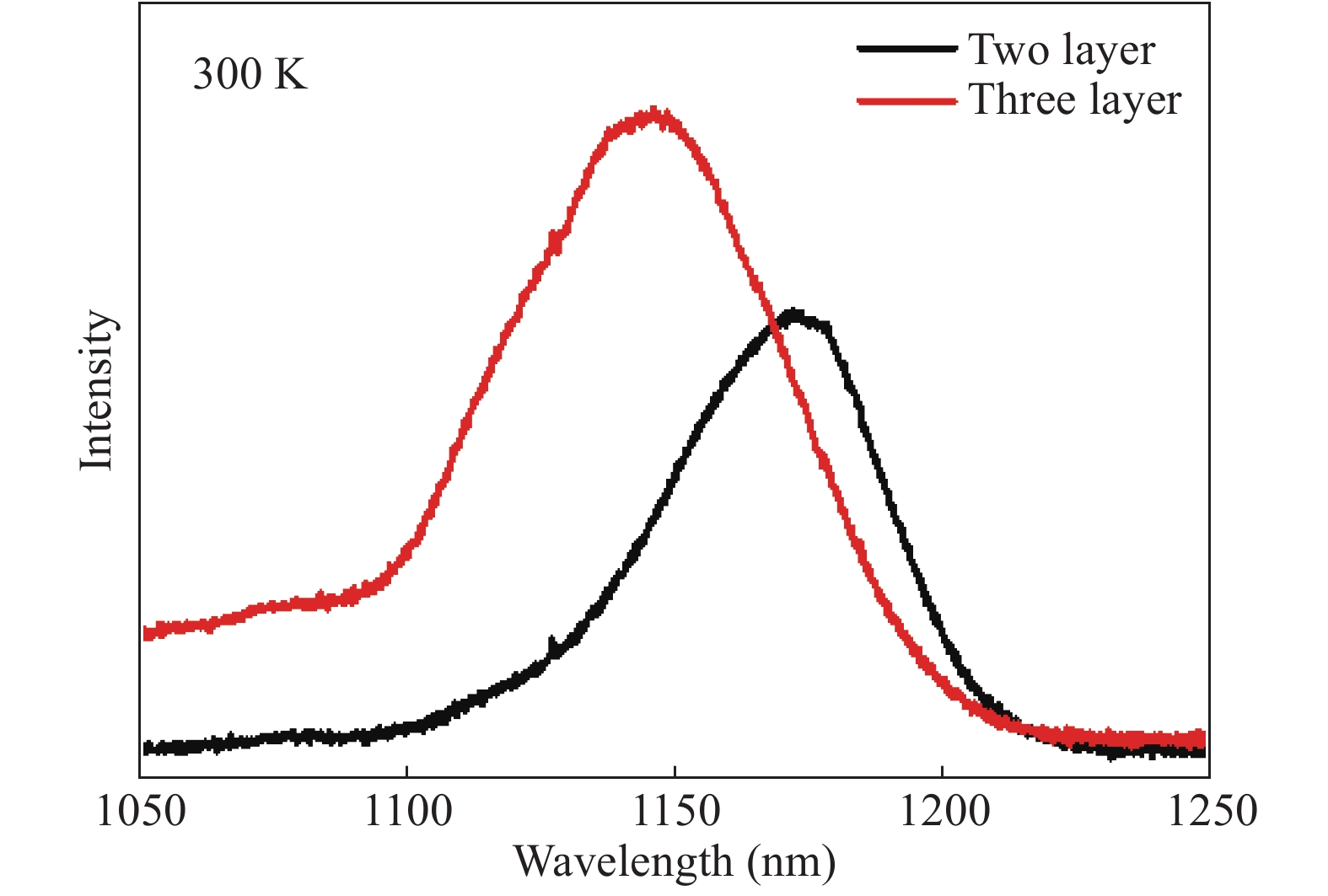
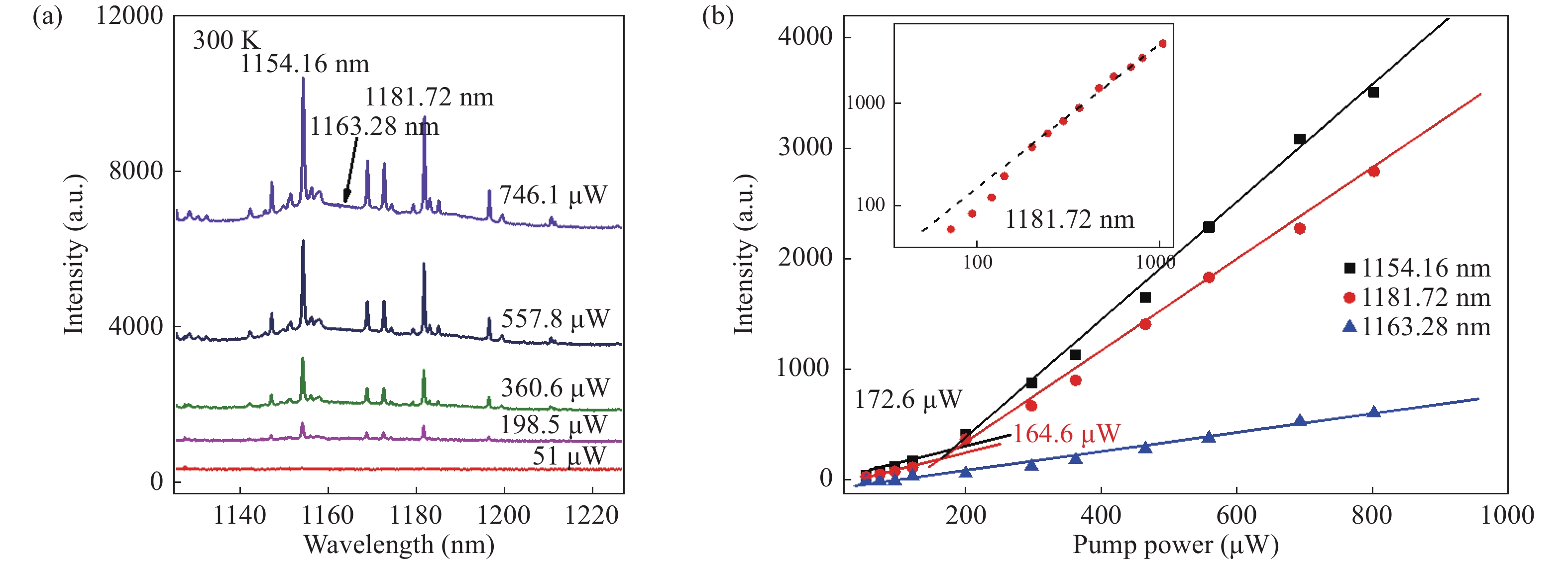
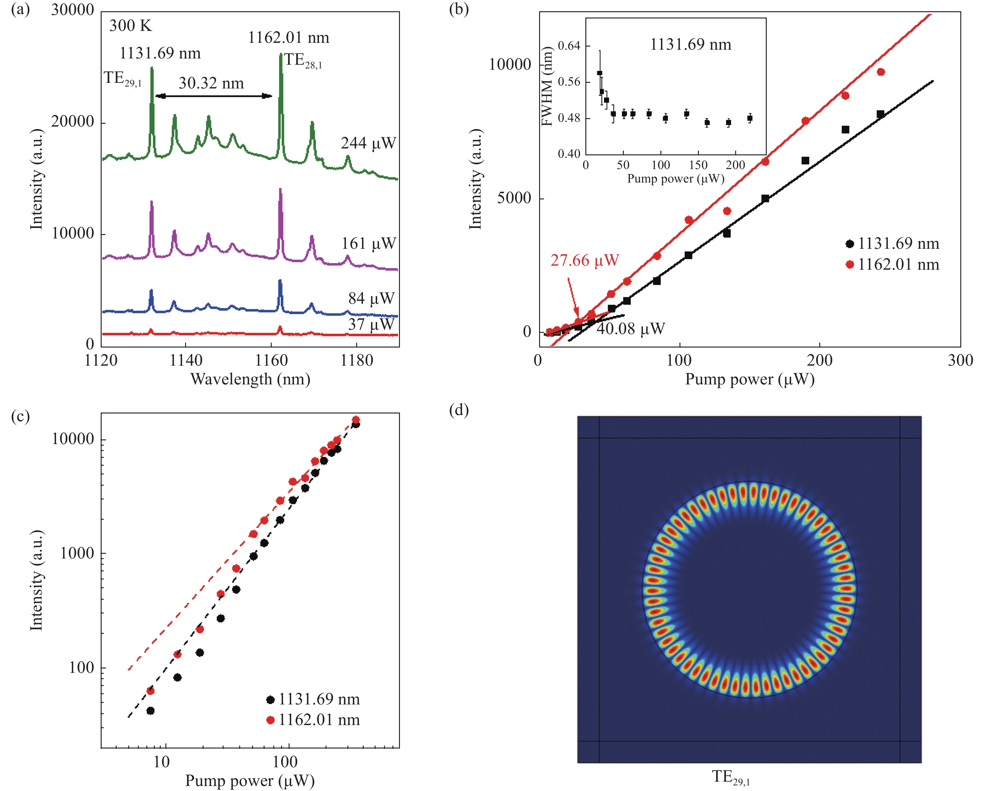
We report on room temperature continuous-wave optically pumped InAs/GaAs quantum dot whispering gallery mode microdisk lasers, heterogeneously integrated on silica/silicon chips. The microdisks are fabricated by photolithography and inductively coupled plasma etching. The lasing wavelength is approximately 1200 nm and the obtained lowest laser threshold is approximately 28 μW. The experimental results show an approach of possible integrated III–V optical active materials on silica/silicon chip for low threshold WGM microdisk lasers.
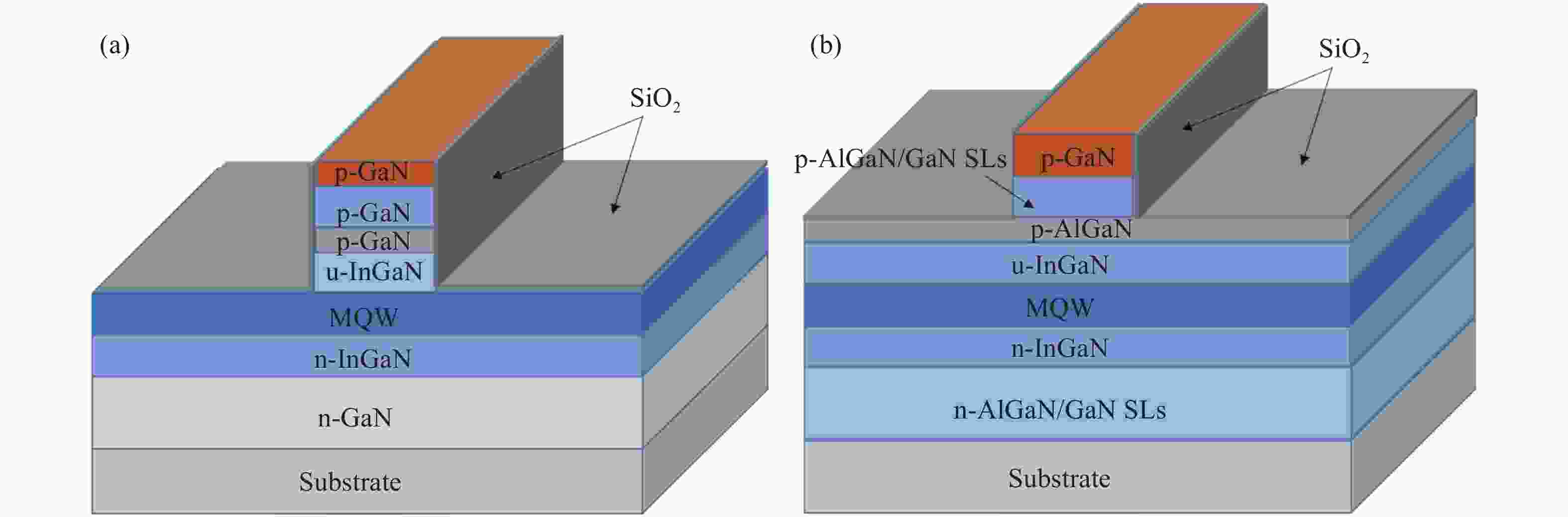
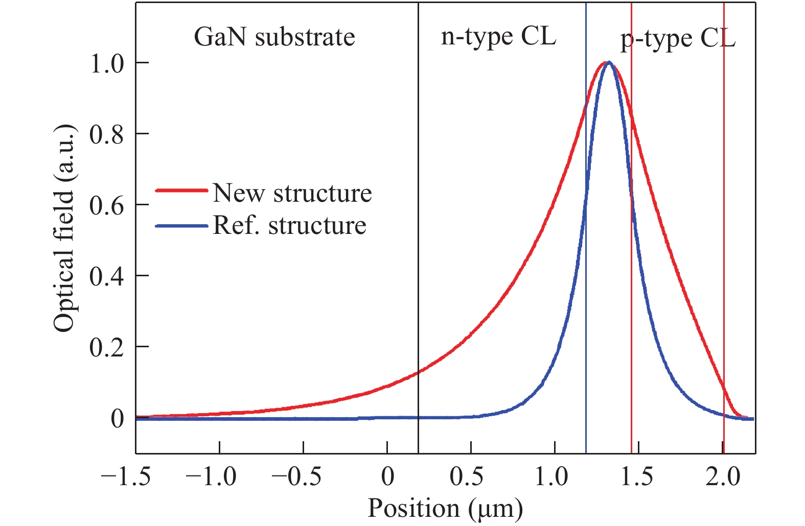
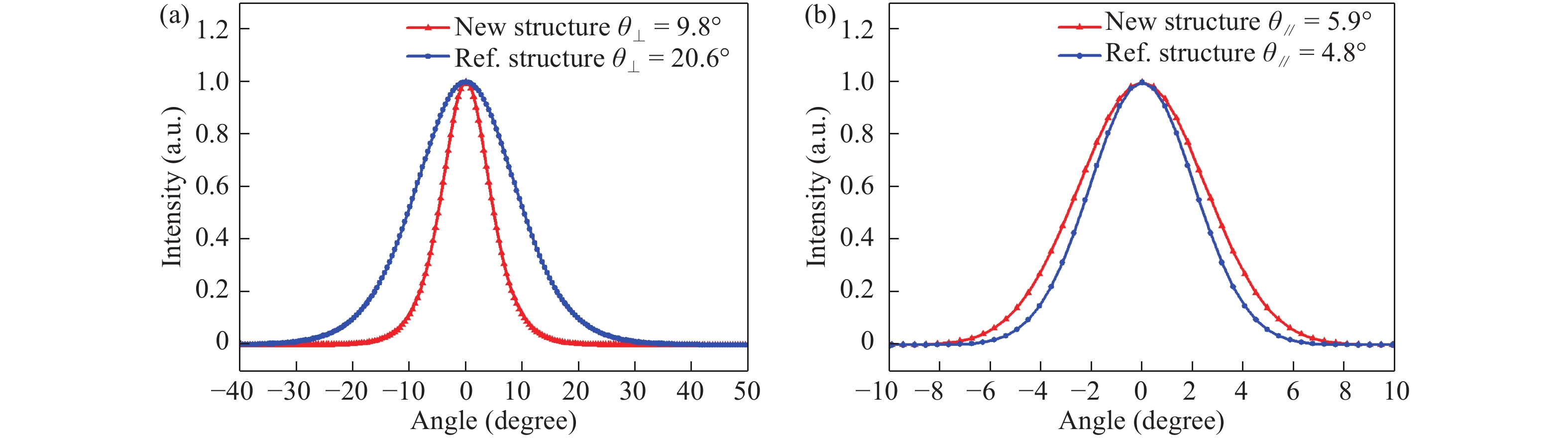
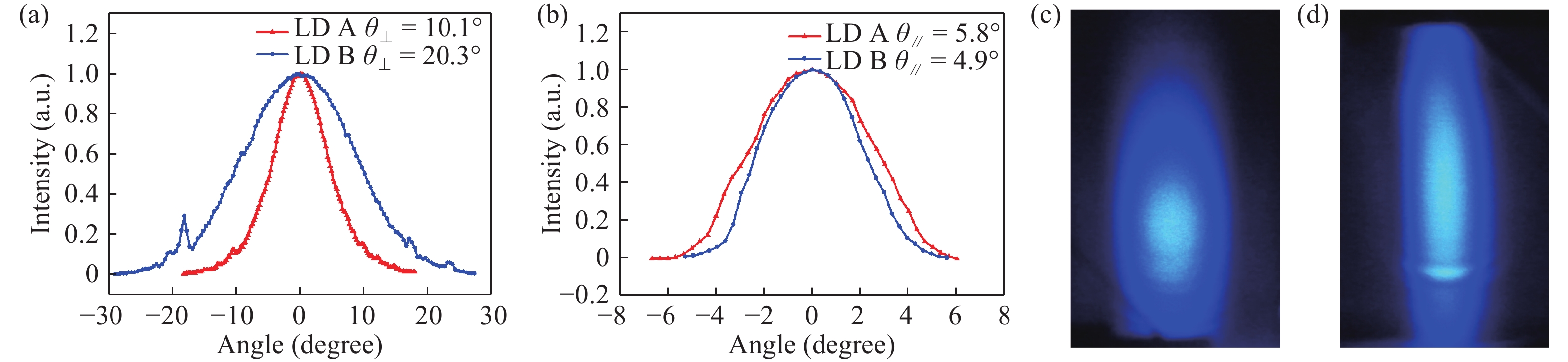
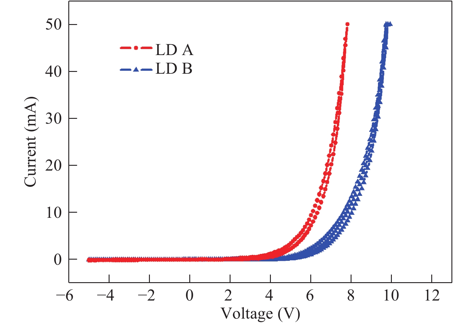
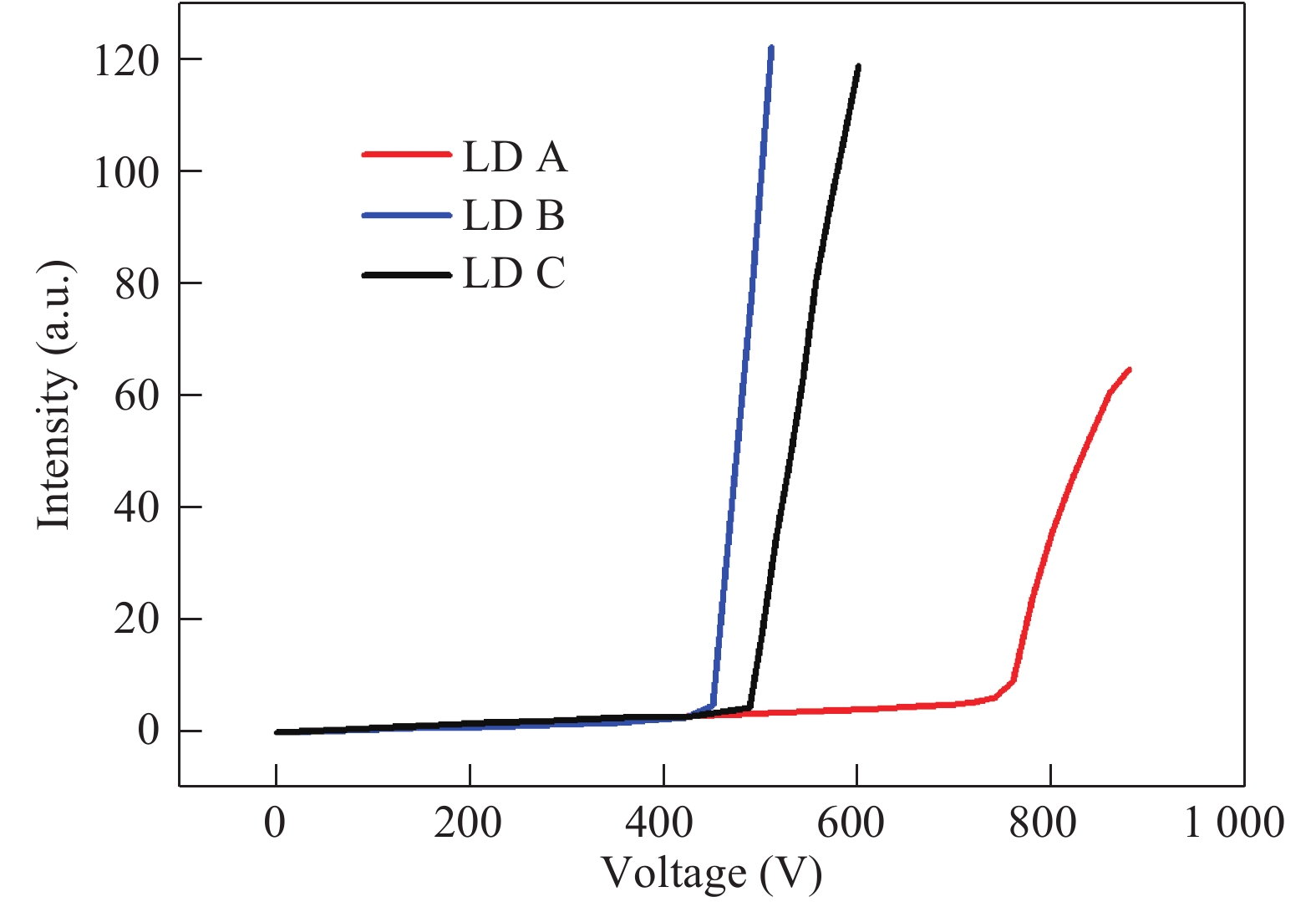
c-plane GaN-based blue laser diodes (LDs) were fabricated with Al-free cladding layers (CLs) and deepened etching depth of mesa structure, so the aspect ratio of the far-field pattern (FFP) of the laser beam can be reduced to as low as 1.7, which is nearly the same as conventional AlGaInP-based red LDs. By using GaN CLs, the radiation angle of the laser beam θ⊥ is only 10.1° in the direction perpendicular to the junction plane. After forming a deeply etched mesa, the beam divergence angle parallel to the junction plane of FFP, θ//, increases from 4.9° to 5.8°. After using the modified structure, the operation voltage of LD is effectively reduced by 2 V at an injection current of 50 mA, but the threshold current value increases. The etching damage may be one of the main reasons responsible for the increase of the threshold current.
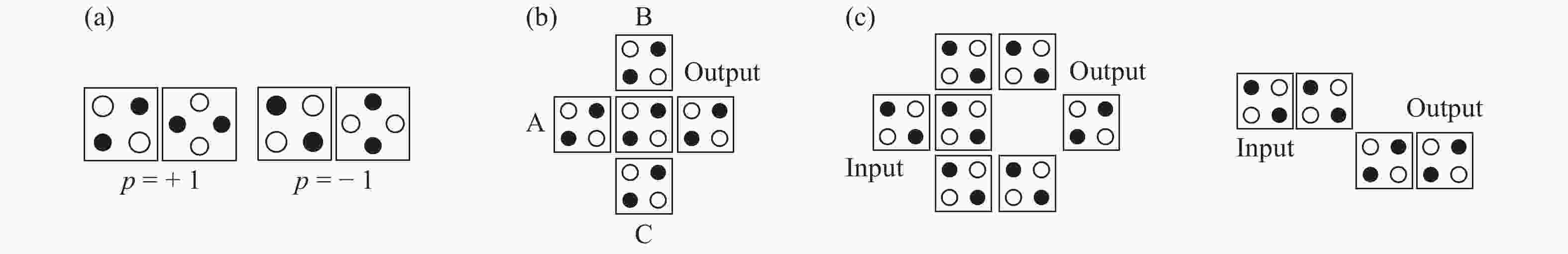
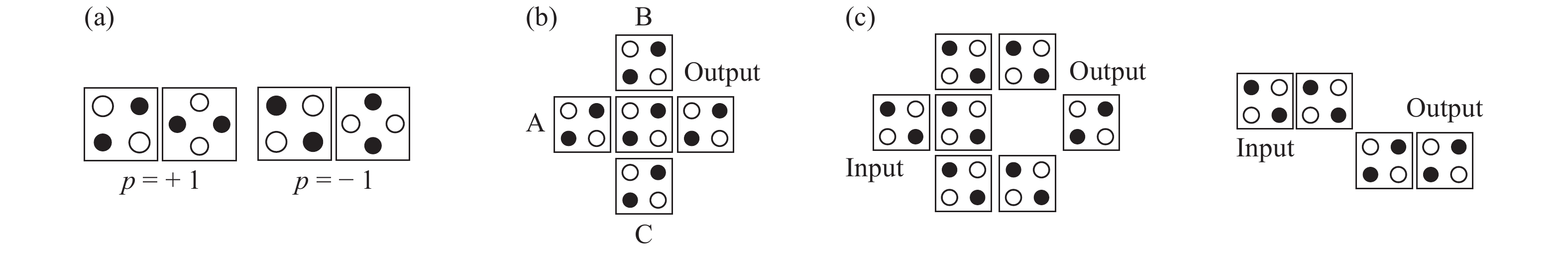
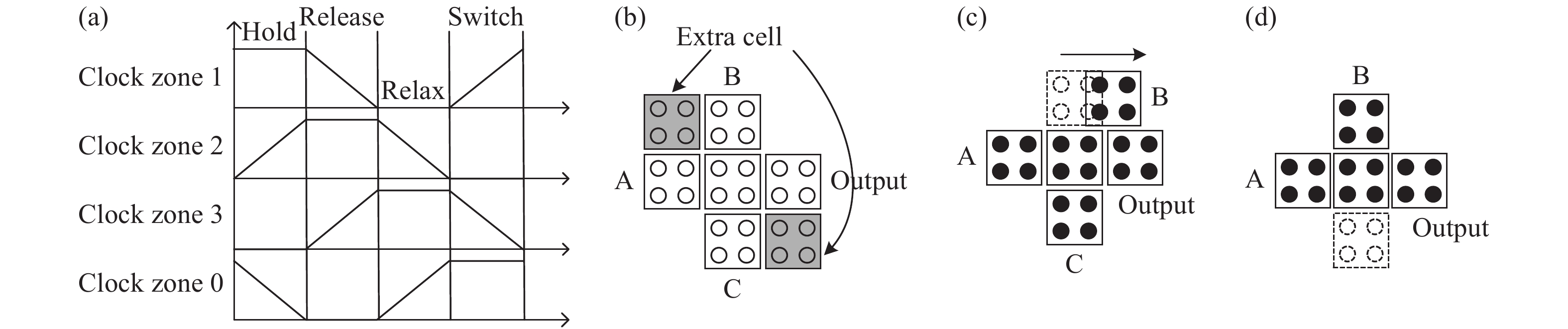
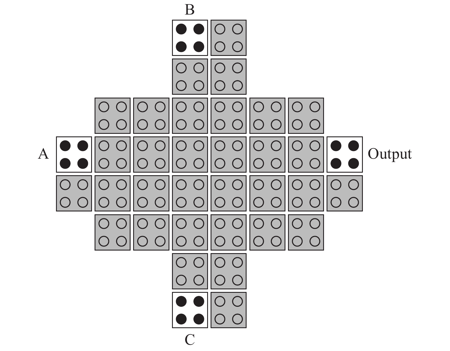
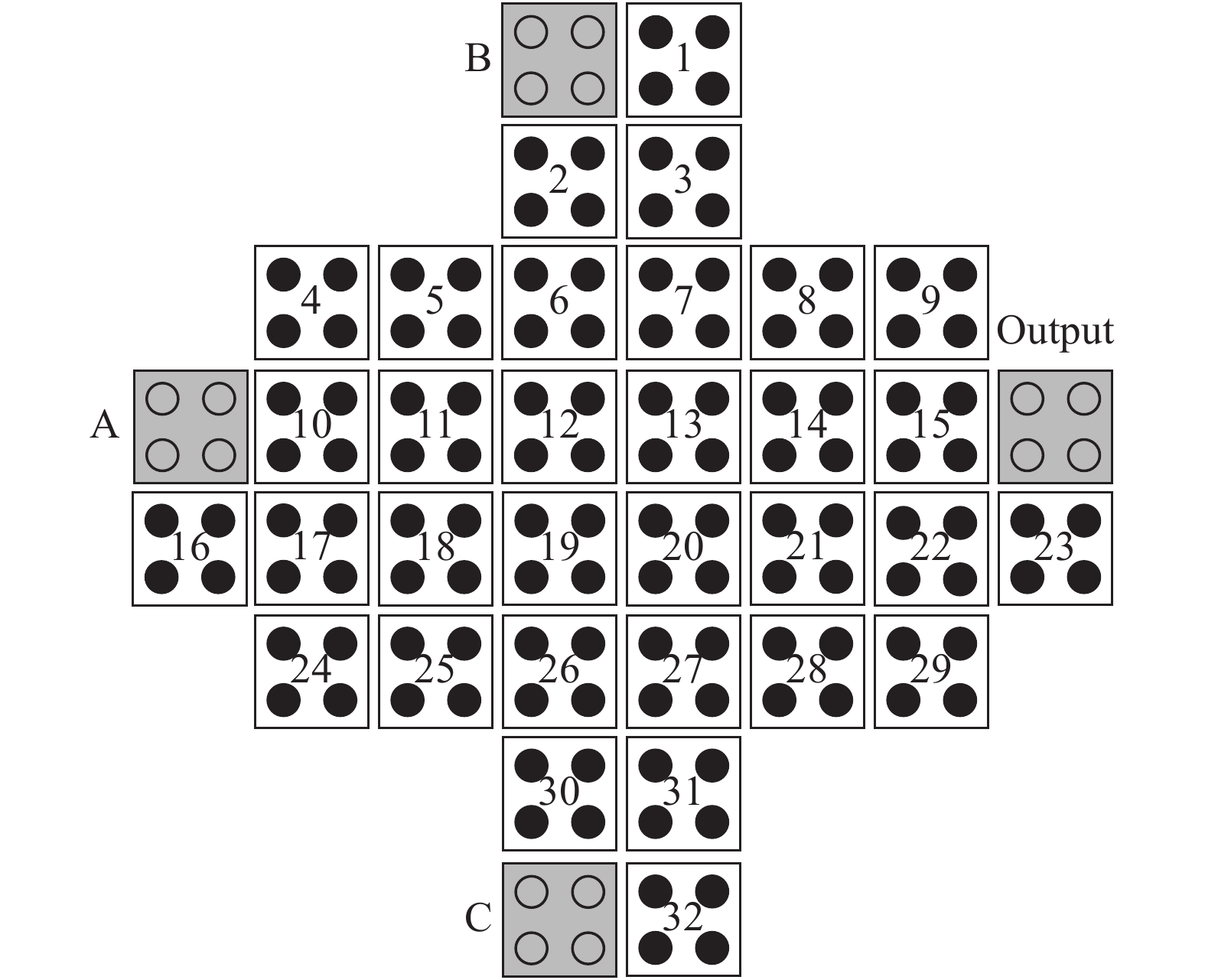
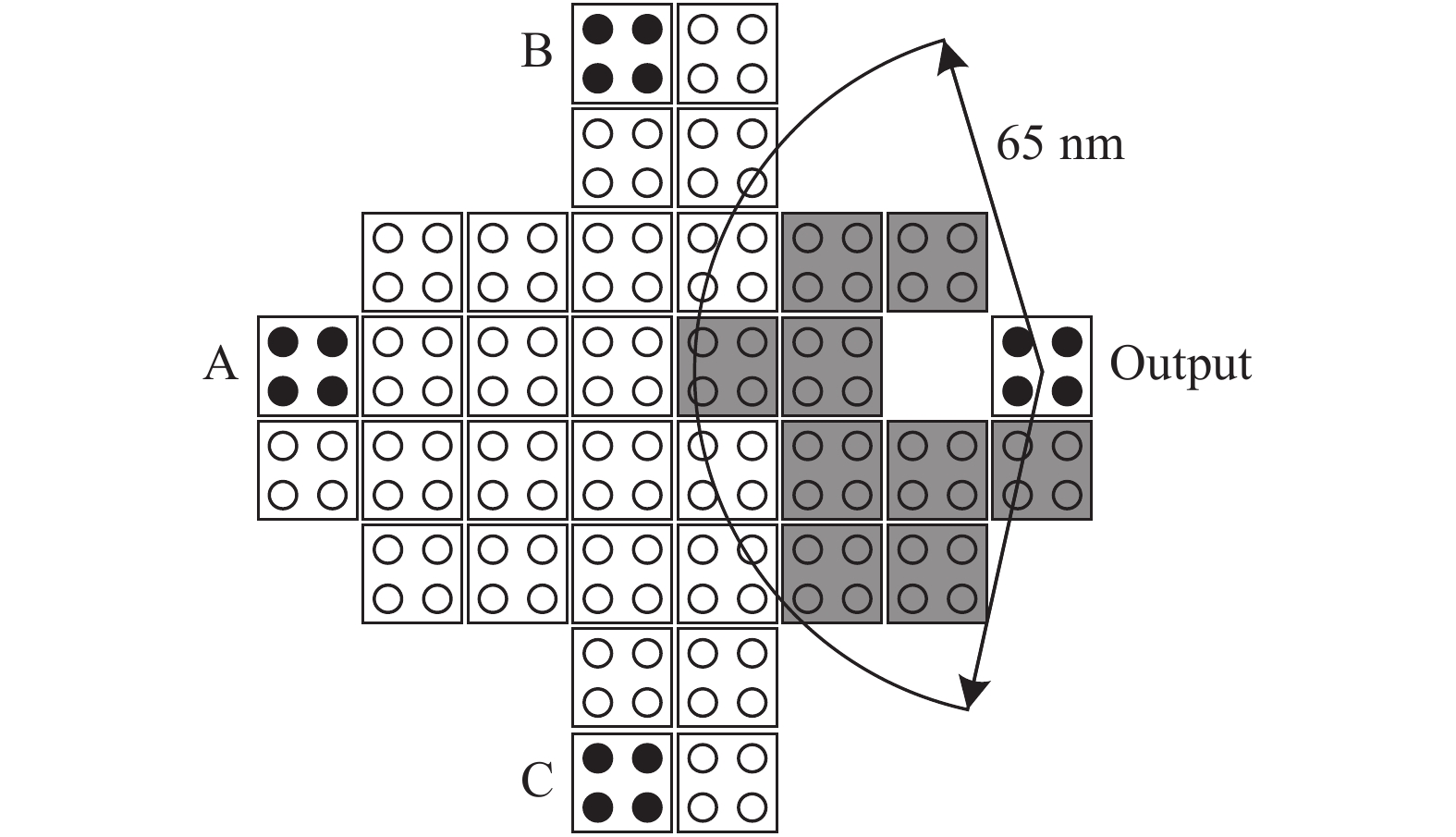
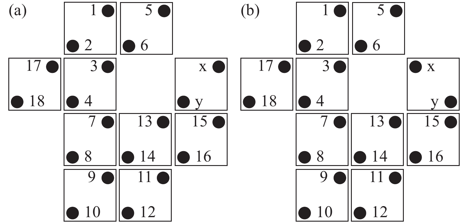
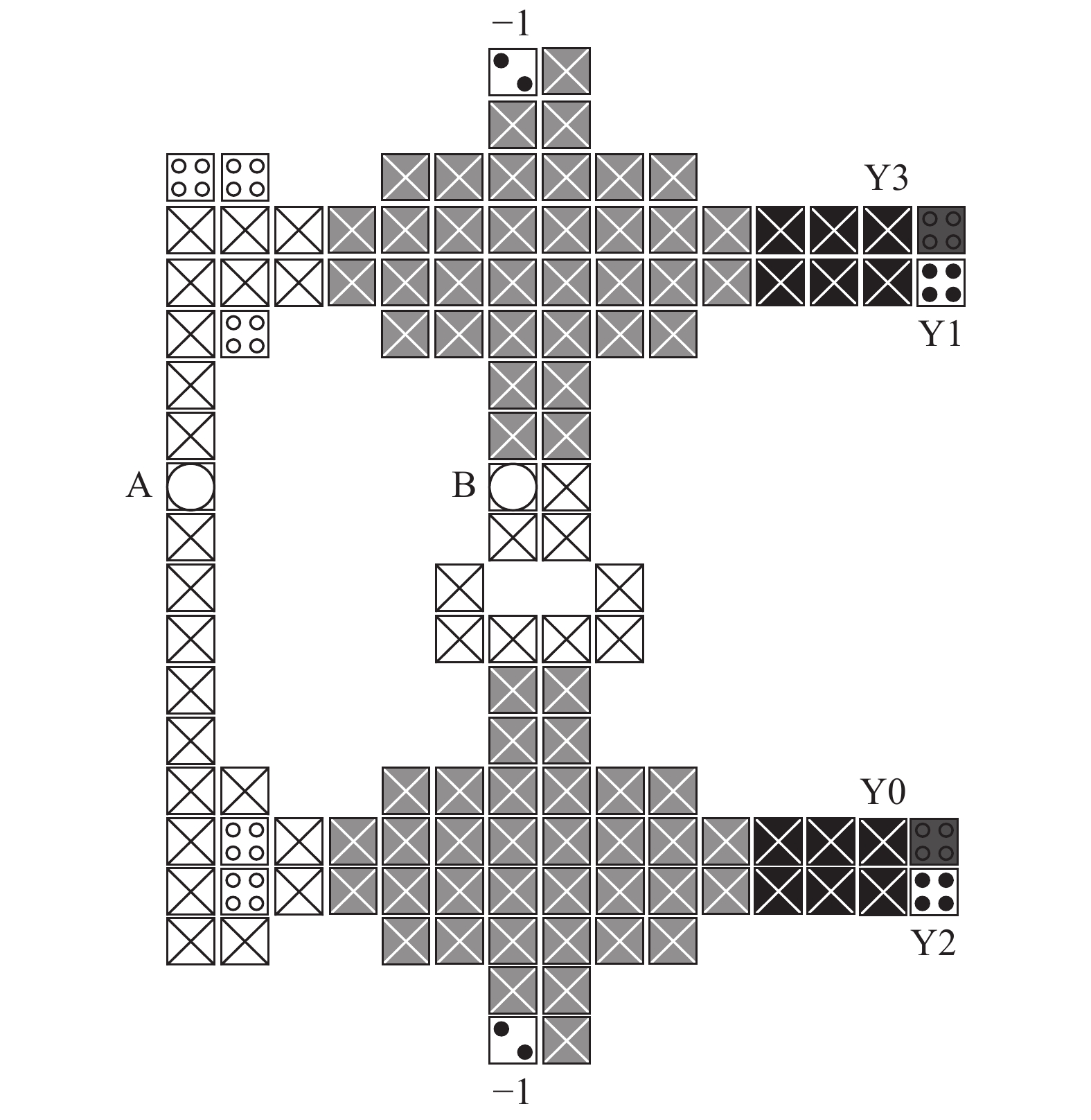
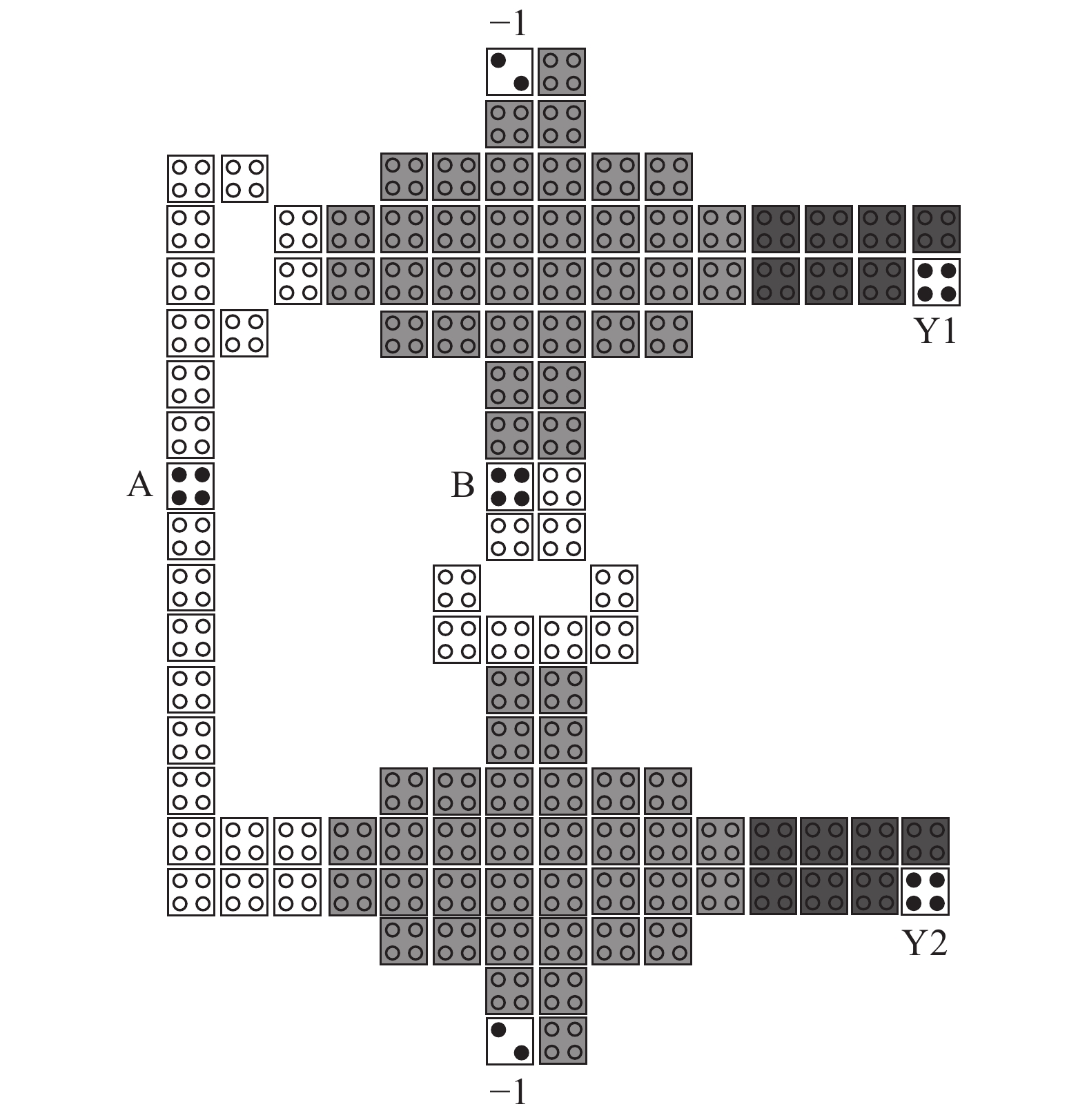
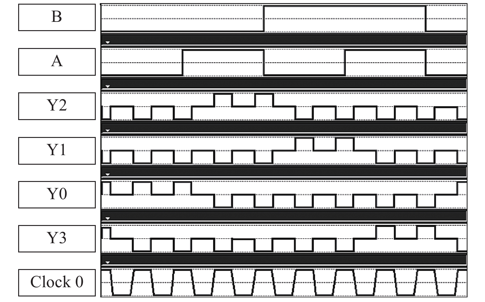
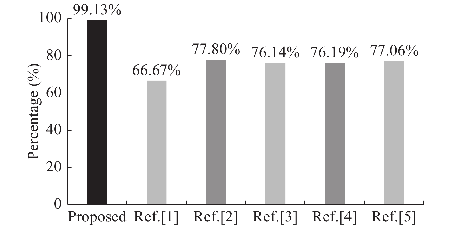
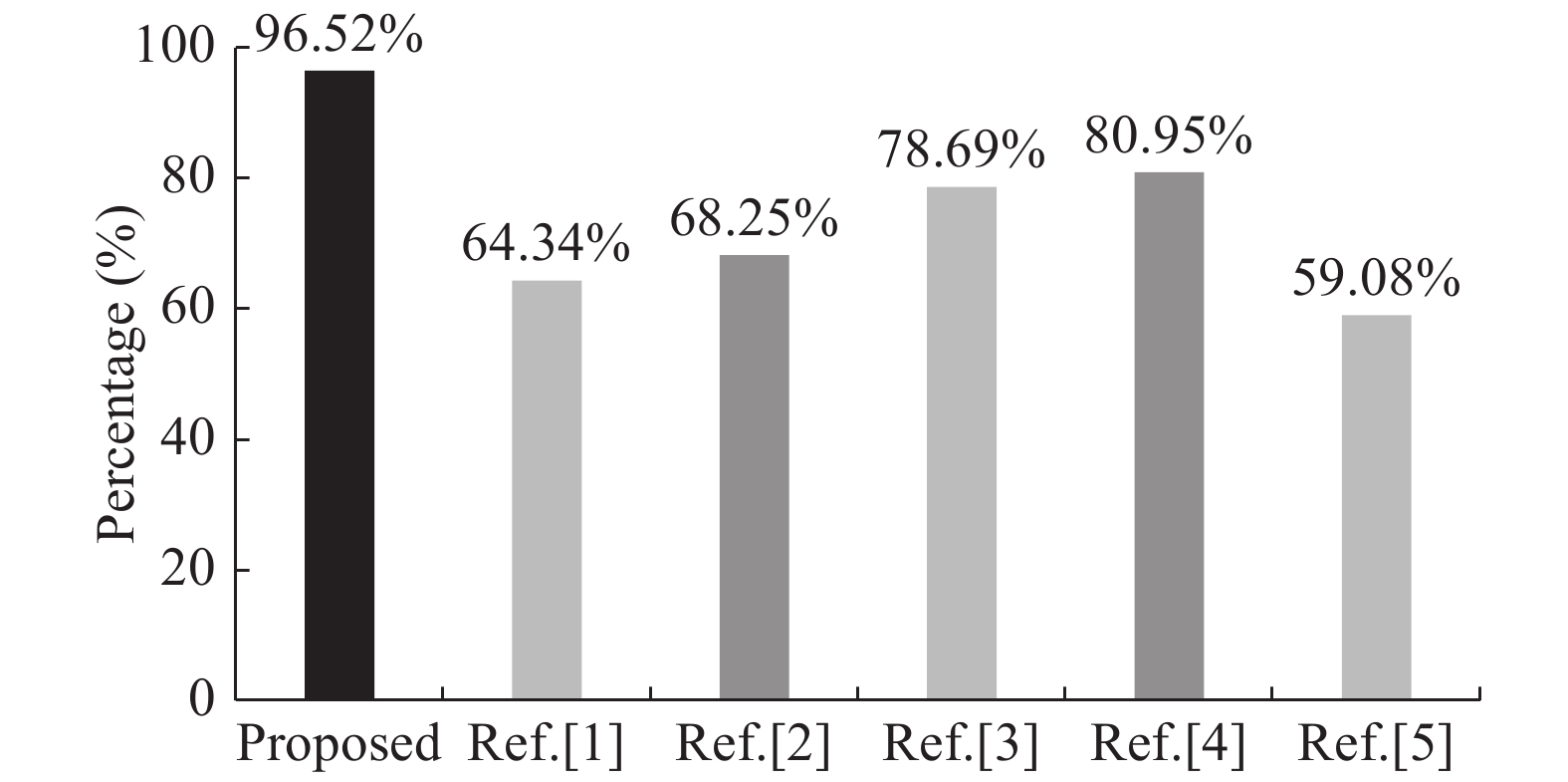
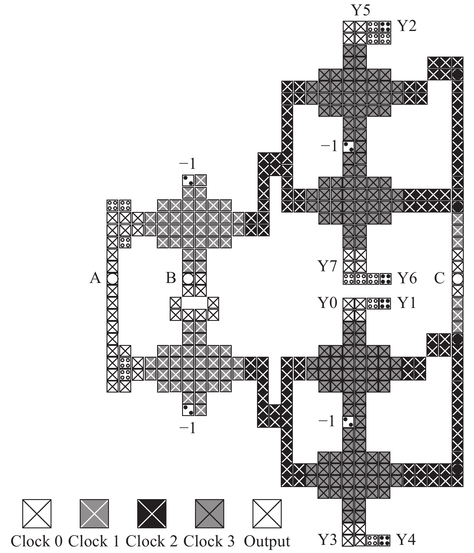
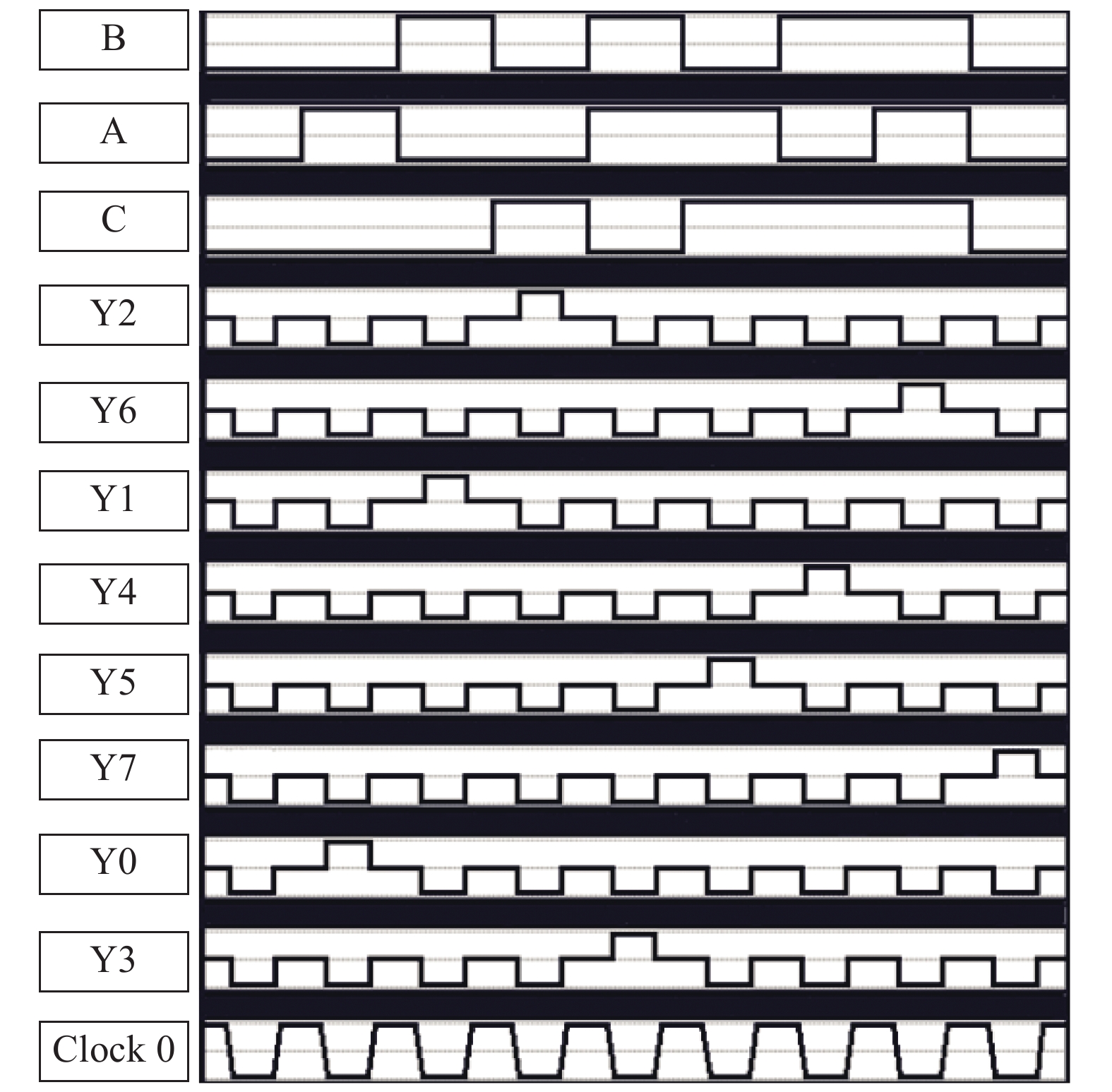
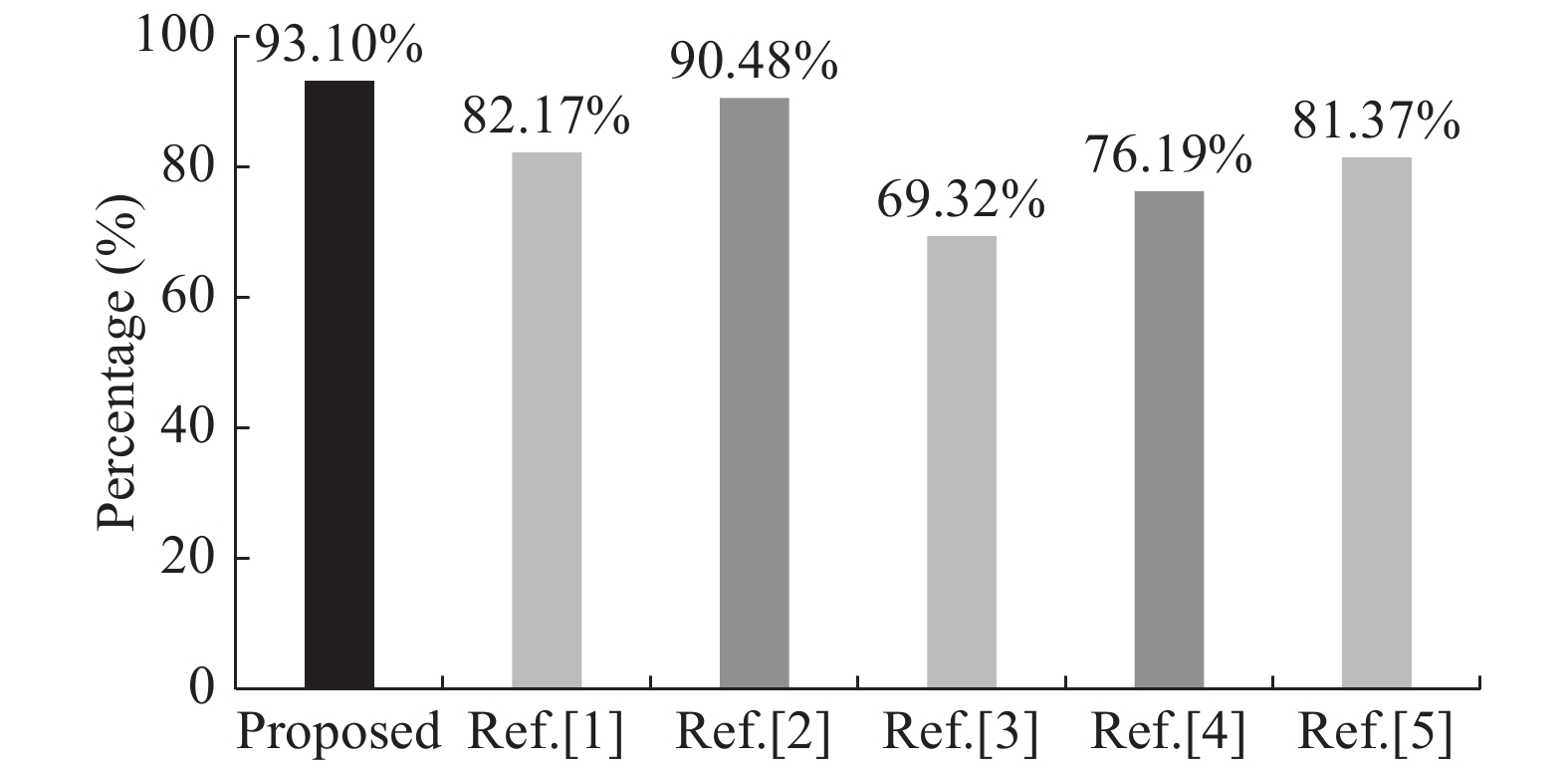
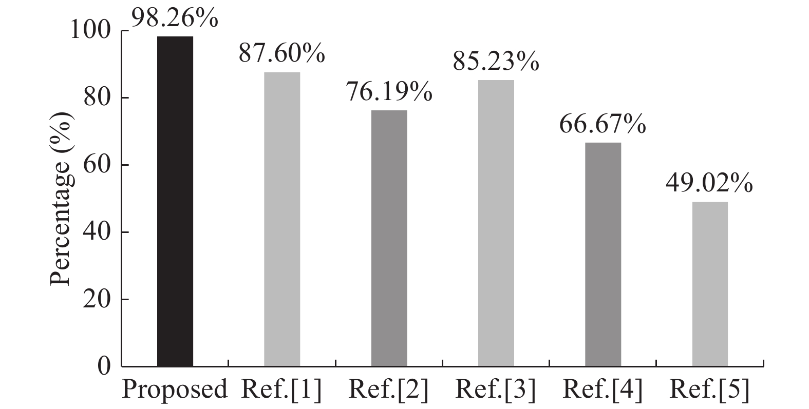
Quantum-dot cellular automata (QCA) is increasingly valued by researchers because of its nanoscale size and very low power consumption. However, in the manufacture of nanoscale devices prone to various forms of defects, which will affect the subsequent circuits design. Therefore, fault-tolerant QCA architectures have become a new research direction. The purpose of this paper is to build a novel fault-tolerant three-input majority gate based on normal cells. Compared with the previous structures, the majority gate shows high fault tolerance under single-cell and double-cell omission defects. In order to examine the functionality of the proposed structure, some physical proofs under single cell missing defects are provided. Besides, two new fault-tolerant decoders are constructed based on the proposed majority gate. In order to fully demonstrate the performance of the proposed decoder, the previous decoders were thoroughly compared in terms of fault tolerance, area and delay. The result shows that the proposed design has a good fault tolerance characteristic, while the performance in other aspects is also quite good.
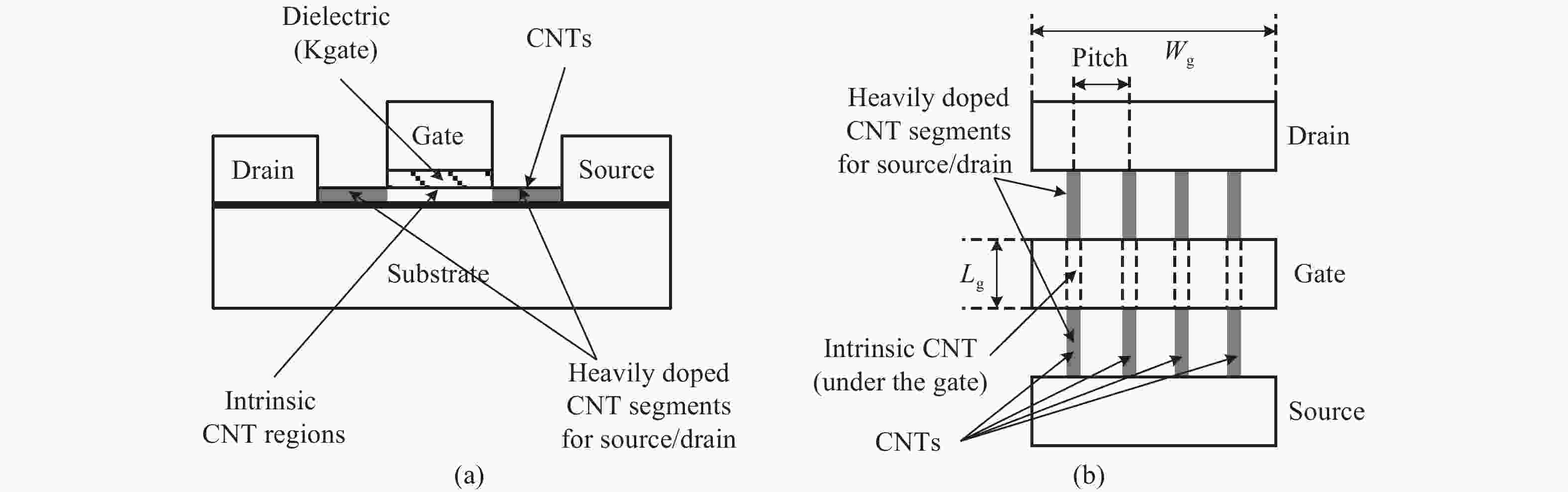
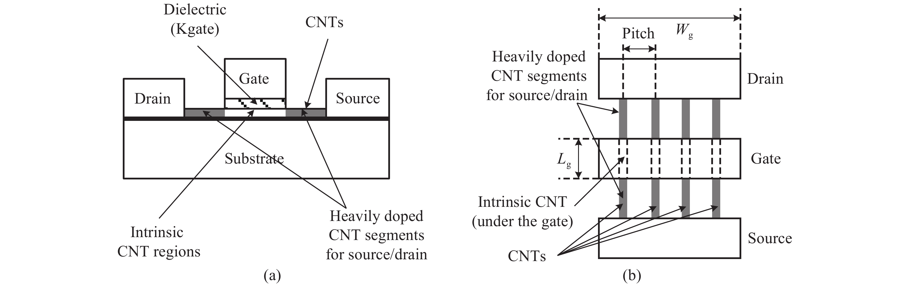
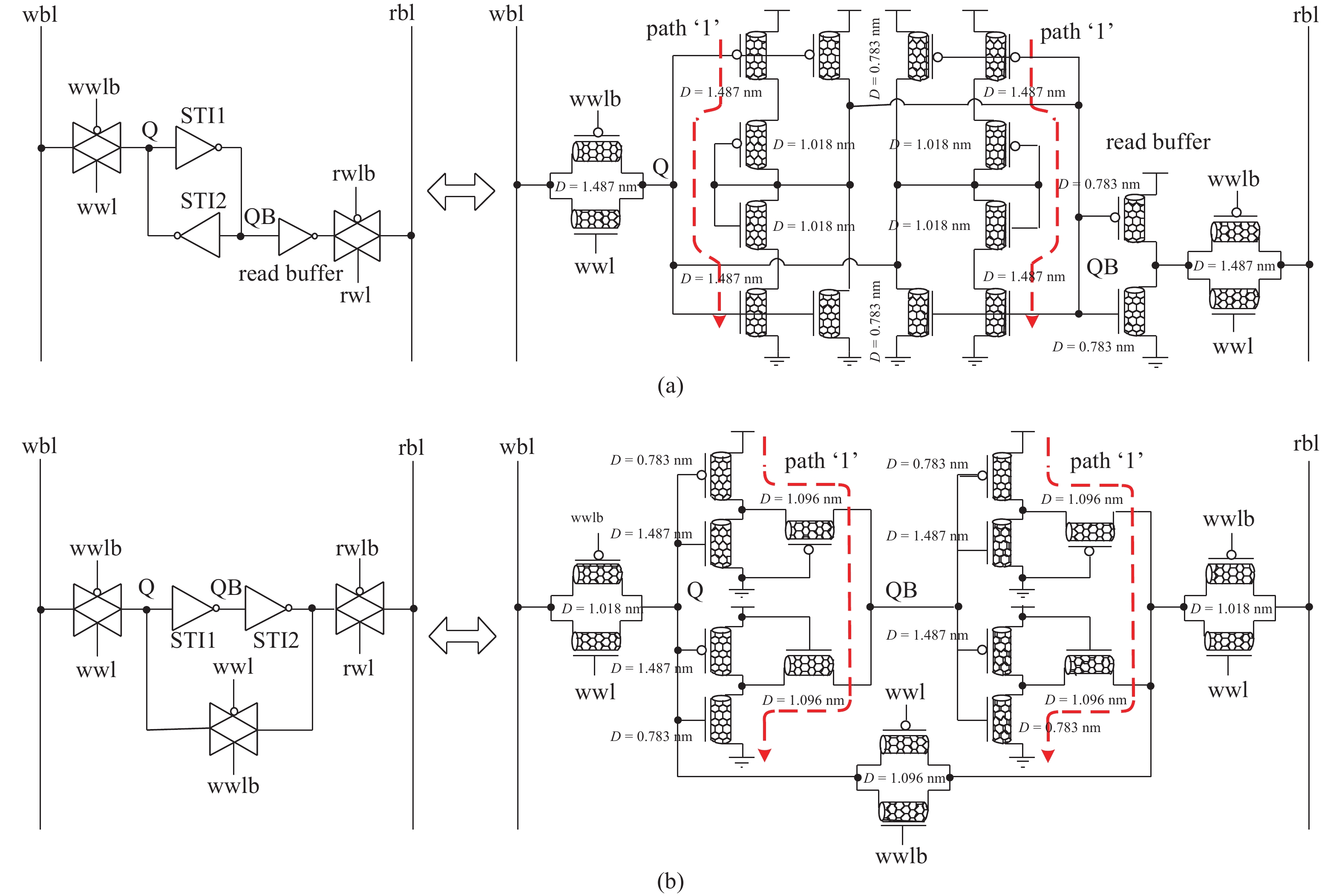
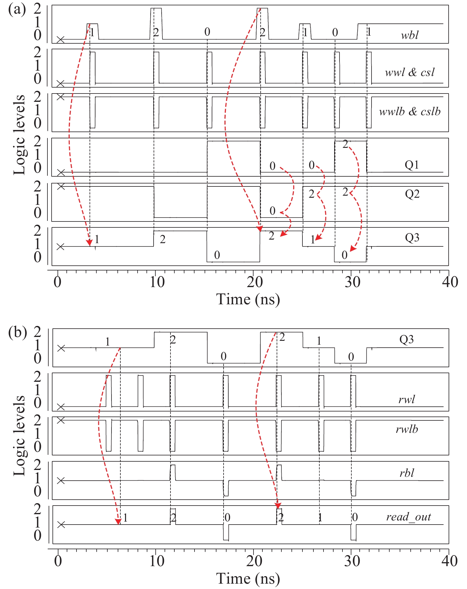
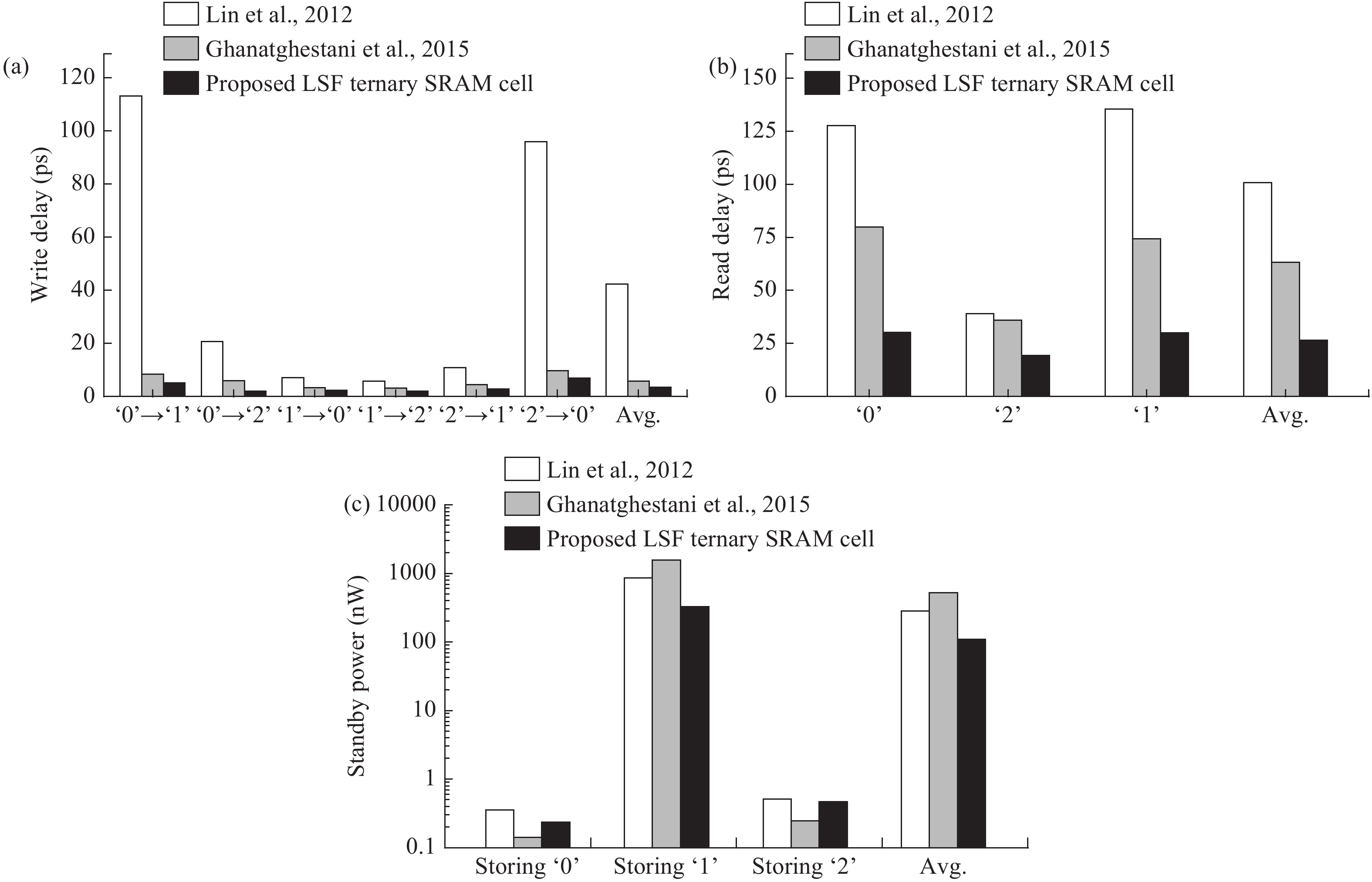
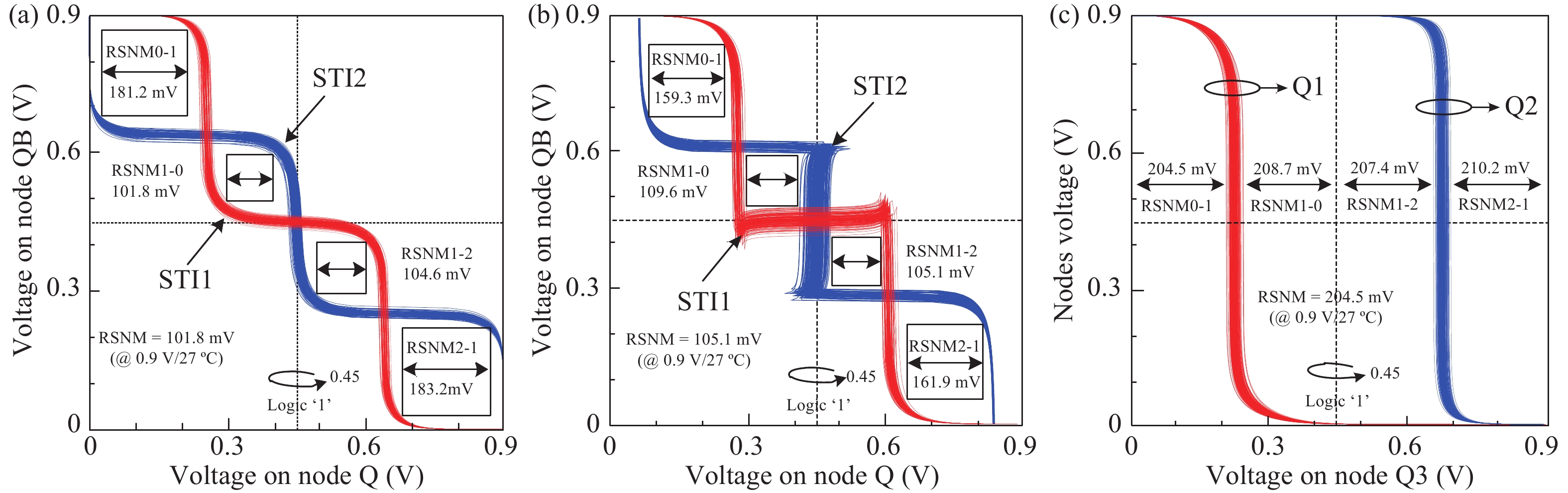
Power dissipation, speed and stability are the most important parameters for multiple-valued SRAM design. To reduce the power consumption and further improve the performance of the ternary SRAM cell, we propose a low standby-power fast ternary SRAM cell based on carbon nanotube field effect transistors (CNFETs). The performance is simulated in terms of three criteria including standby-power, delay (write and read) and stability (RSNM). Compared to the novel ternary SRAM cell, our results show that the average standby-power, write and read delay of the proposed cell are reduced by 78.1%, 39.6% and 58.2%, respectively. In addition, the RSNM under process variations is 2.01× and 1.95× of the conventional and novel ternary SRAM cells, respectively.
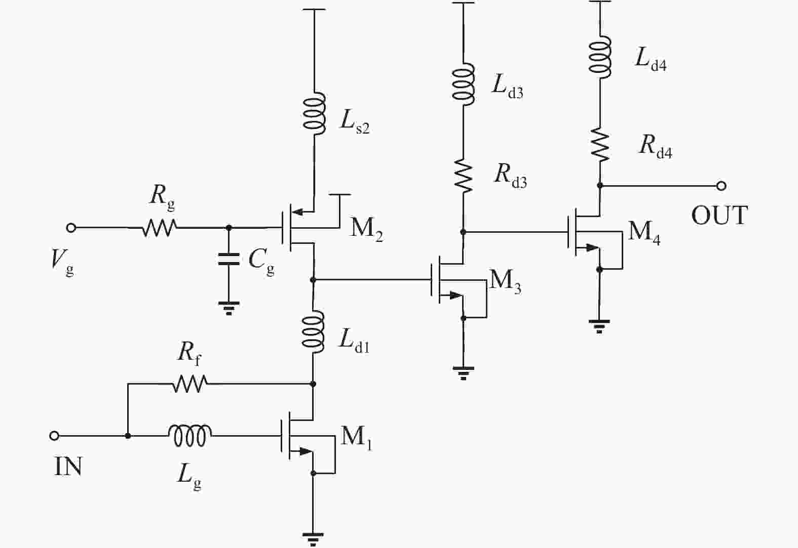
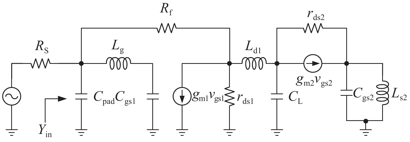
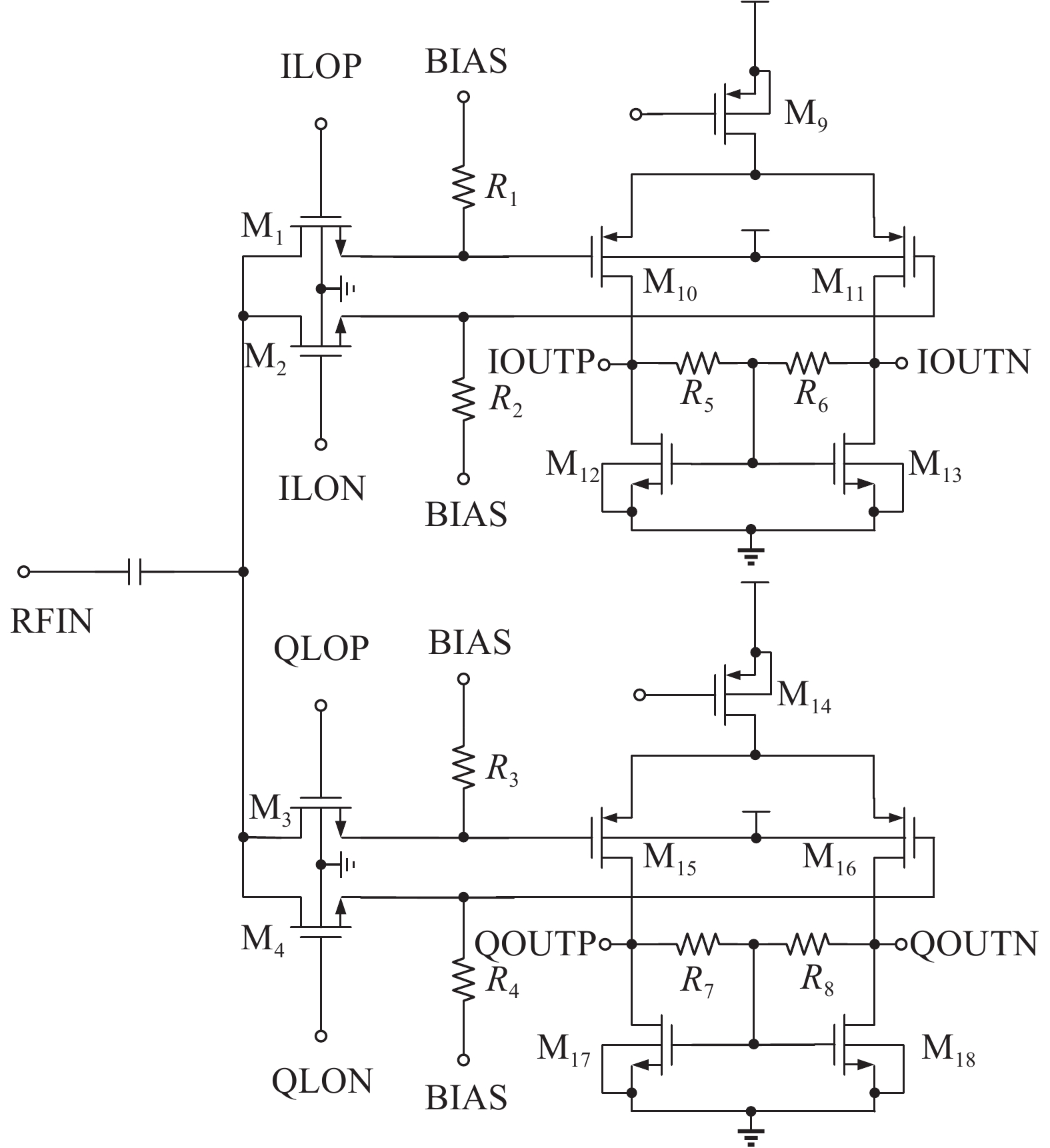
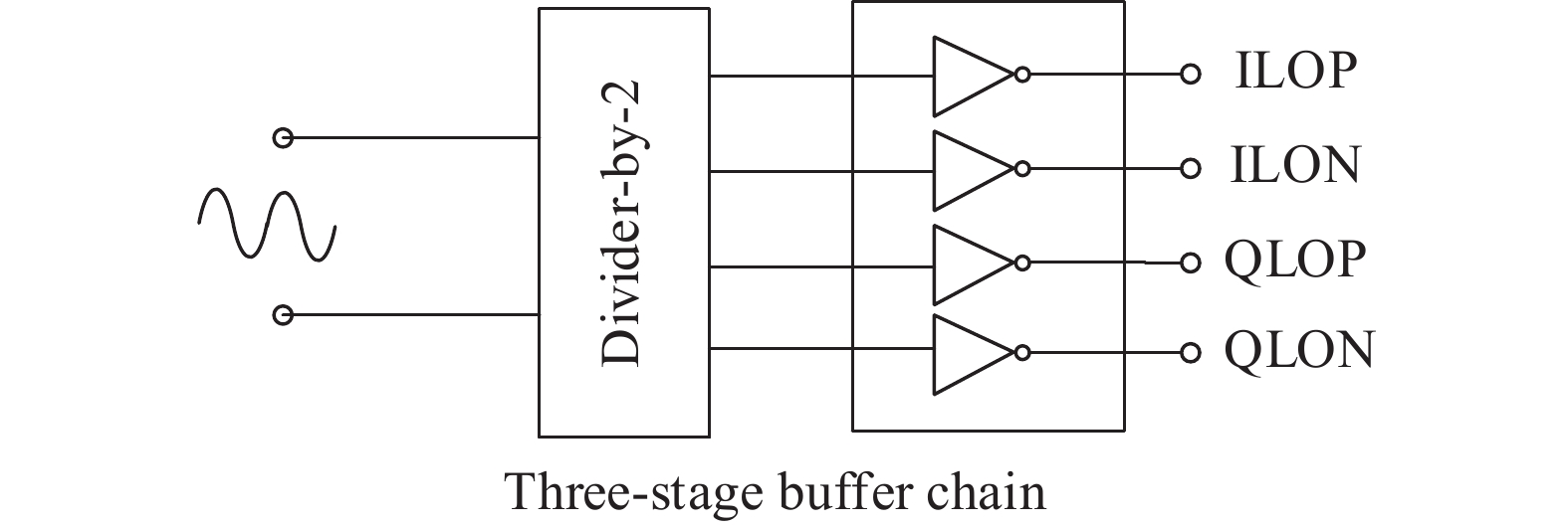
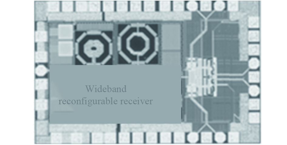
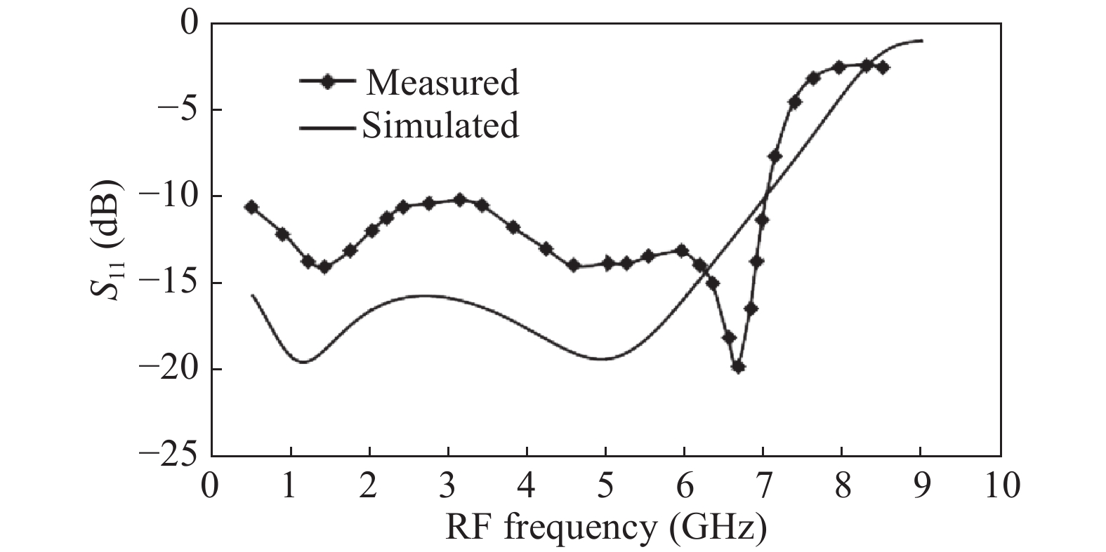
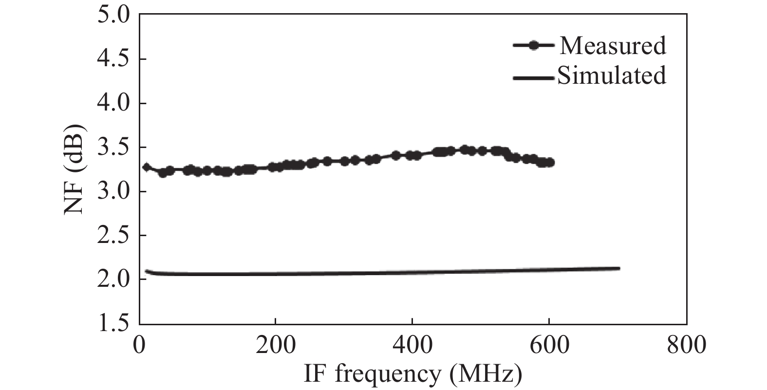
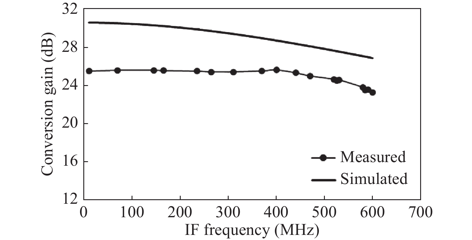
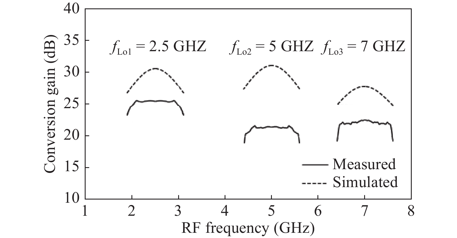
A 0.7–7 GHz wideband RF receiver front-end SoC is designed using the CMOS process. The front-end is composed of two main blocks: a single-ended wideband low noise amplifier (LNA) and an in-phase/quadrature (I/Q) voltage-driven passive mixer with IF amplifiers. Based on a self-biased resistive negative feedback topology, the LNA adopts shunt-peaking inductors and a gate inductor to boost the bandwidth. The passive down-conversion mixer includes two parts: passive switches and IF amplifiers. The measurement results show that the front-end works well at different LO frequencies, and this chip is reconfigurable among 0.7 to 7 GHz by tuning the LO frequency. The measured results under 2.5-GHz LO frequency show that the front-end SoC achieves a maximum conversion gain of 26 dB, a minimum noise figure (NF) of 3.2 dB, with an IF bandwidth of greater than 500 MHz. The chip area is 1.67 × 1.08 mm2.

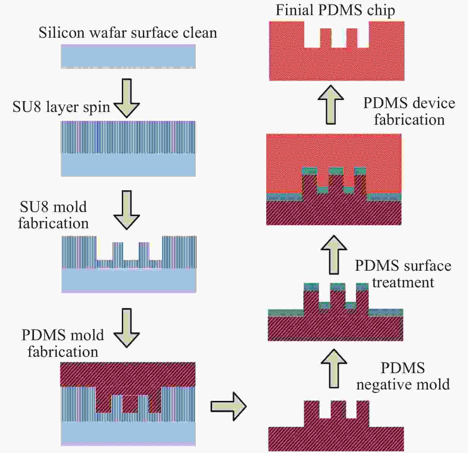
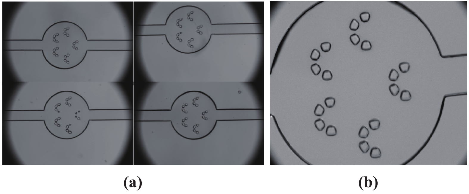
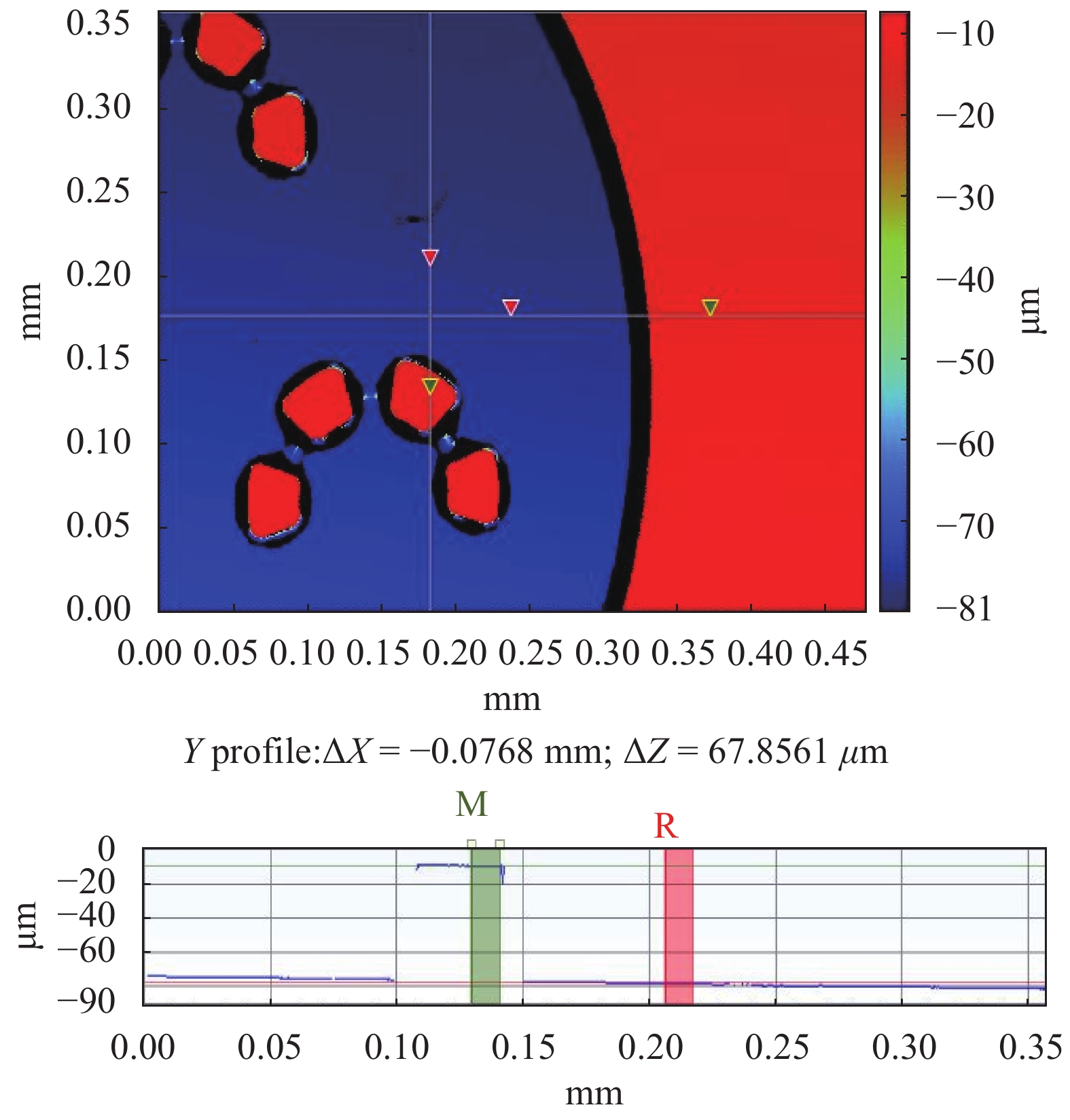
High aspect ratio units are necessary parts of complex microstructures in microfluidic devices. Some methods that are available to achieve a high aspect ratio require expensive materials or complex chemical processes; for other methods it is difficult to reach simple high aspect ratio structures, which need supporting structures. The paper presents a simple and cheap two-step Polydimethylsioxane (PDMS) transferring process to get high aspect ratio single pillars, which only requires covering the PDMS mold with a Brij@52 surface solution after getting a relative PDMS mold based on an SU8 mold. The experimental results demonstrate the method efficiency and effectiveness.
.jpg)


