


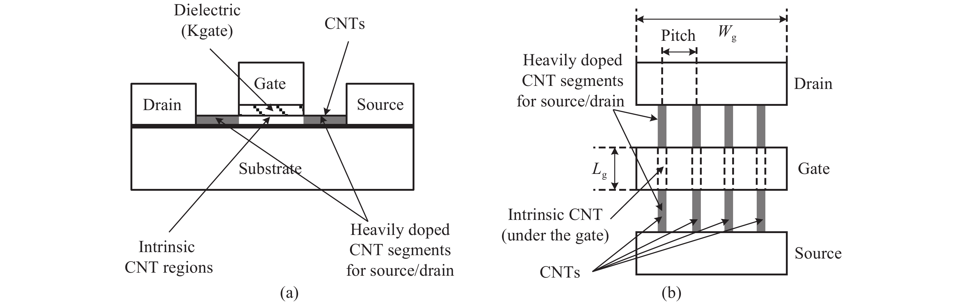
Fig. 1.
Schematic diagrams of a typical carbon nanotube transistor. (a) Cross sectional view. (b) Top view.
SEMICONDUCTOR INTEGRATED CIRCUITS
Gang Li1, Pengjun Wang1, 2, , Yaopeng Kang1 and Yuejun Zhang1
Corresponding author: Pengjun Wang, Email: wangpengjun@nbu.edu.cn
Abstract: Power dissipation, speed and stability are the most important parameters for multiple-valued SRAM design. To reduce the power consumption and further improve the performance of the ternary SRAM cell, we propose a low standby-power fast ternary SRAM cell based on carbon nanotube field effect transistors (CNFETs). The performance is simulated in terms of three criteria including standby-power, delay (write and read) and stability (RSNM). Compared to the novel ternary SRAM cell, our results show that the average standby-power, write and read delay of the proposed cell are reduced by 78.1%, 39.6% and 58.2%, respectively. In addition, the RSNM under process variations is 2.01× and 1.95× of the conventional and novel ternary SRAM cells, respectively.
Keywords: CNFETs, ternary SRAM cell, low standby-power, high stability
| [1] |
Cho G, Lombardi F. Design and process variation analysis of CNTFET-based ternary memory cells. Integr VLSI J, 2011, 54(C): 97
|
| [2] |
Kamar Z, Nepal K. Noise margin-optimized ternary CMOS SRAM delay and sizing characteristics. IEEE International Midwest Symposium on Circuits and Systems (MWSCAS), 2010: 801
|
| [3] |
Zhang Y J, Wang P J, Xiong B Y, et al. Design of a high information-density multiple valued 2-read 1-write register file. IEICE Electron Express, 2012, 9(11): 958 doi: 10.1587/elex.9.958
|
| [4] |
Appenzeller J. Carbon nanotubes for high-performance electronics—progress and prospect. Proc IEEE, 2008, 96(2): 201 doi: 10.1109/JPROC.2007.911051
|
| [5] |
Lin Y M, Appenzeller J, Knoch J, et al. High performance carbon nanotube field-effect transistor with tunable polarities. IEEE Trans Nanotechnol, 2005, 4(5): 481 doi: 10.1109/TNANO.2005.851427
|
| [6] |
Qiu C, Zhang Z, Xiao M, et al. Scaling carbon nanotube complementary transistors to 5-nm gate lengths. Science, 2017, 355(6322): 271 doi: 10.1126/science.aaj1628
|
| [7] |
You K, Nepal K. Design of a ternary static memory cell using carbon nanotube-based transistors. IET Micro & Nano Lett, 2011, 6(6): 381
|
| [8] |
Lin S, Kim Y B, Lombardi F. Design of a ternary memory cell using CNTFETs. IEEE Trans Nanotechnol, 2012, 11(5): 1019 doi: 10.1109/TNANO.2012.2211614
|
| [9] |
Ghanatghestani M M, Pedram H, Ghavami B. Design of a low-standby power and high-speed ternary memory cell based on carbon nanotube field-effect transistor. J Comput Theor Nanosci, 2015, 12(12): 5457 doi: 10.1166/jctn.2015.4546
|
| [10] |
Ebrahim A, Abdolreza D. A novel design of low power and high read stability ternary SRAM (T-SRAM), memory based on the modified gate diffusion input (m-GDI) method in nanotechnology. Microelectron J, 2016, 58: 44 doi: 10.1016/j.mejo.2016.10.009
|
| [11] |
Shin K, Choi W, Park J. Half-select free and bit-line sharing 9T SRAM for reliable supply voltage scaling. IEEE Trans Circ Syst I, 2017, 64(8): 2036
|
| [12] |
Deng J, Wong H S P. A compact SPICE model for carbon-nanotube field effect transistors including nonidealities and its application-part II: model of the intrinsic channel region. IEEE Trans Electron Devices, 2007, 54(12): 3186 doi: 10.1109/TED.2007.909030
|
| [13] |
Tabrizchi S, Azimi N, Navi K. A novel ternary half adder and multiplier based on carbon nanotube field effect transistors. Front Inform Technol Electron Eng, 2017, 18(3): 423 doi: 10.1631/FITEE.1500366
|
| [14] |
Prabhu C M R, Singh A K. Low-power fast (LPF) SRAM cell for write/read operation. IEICE Electron Express, 2011, 8(18): 1473 doi: 10.1587/elex.8.1473
|
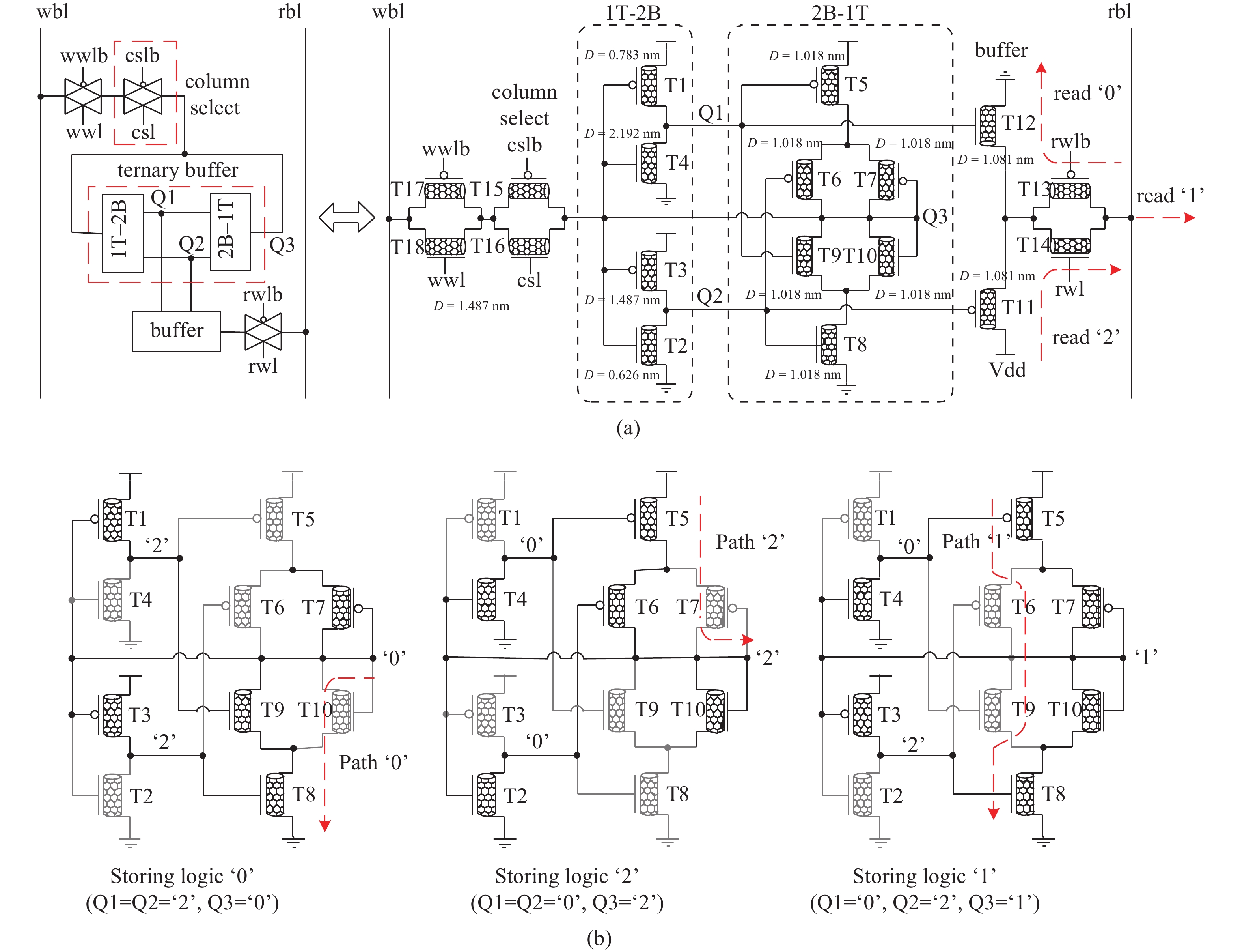
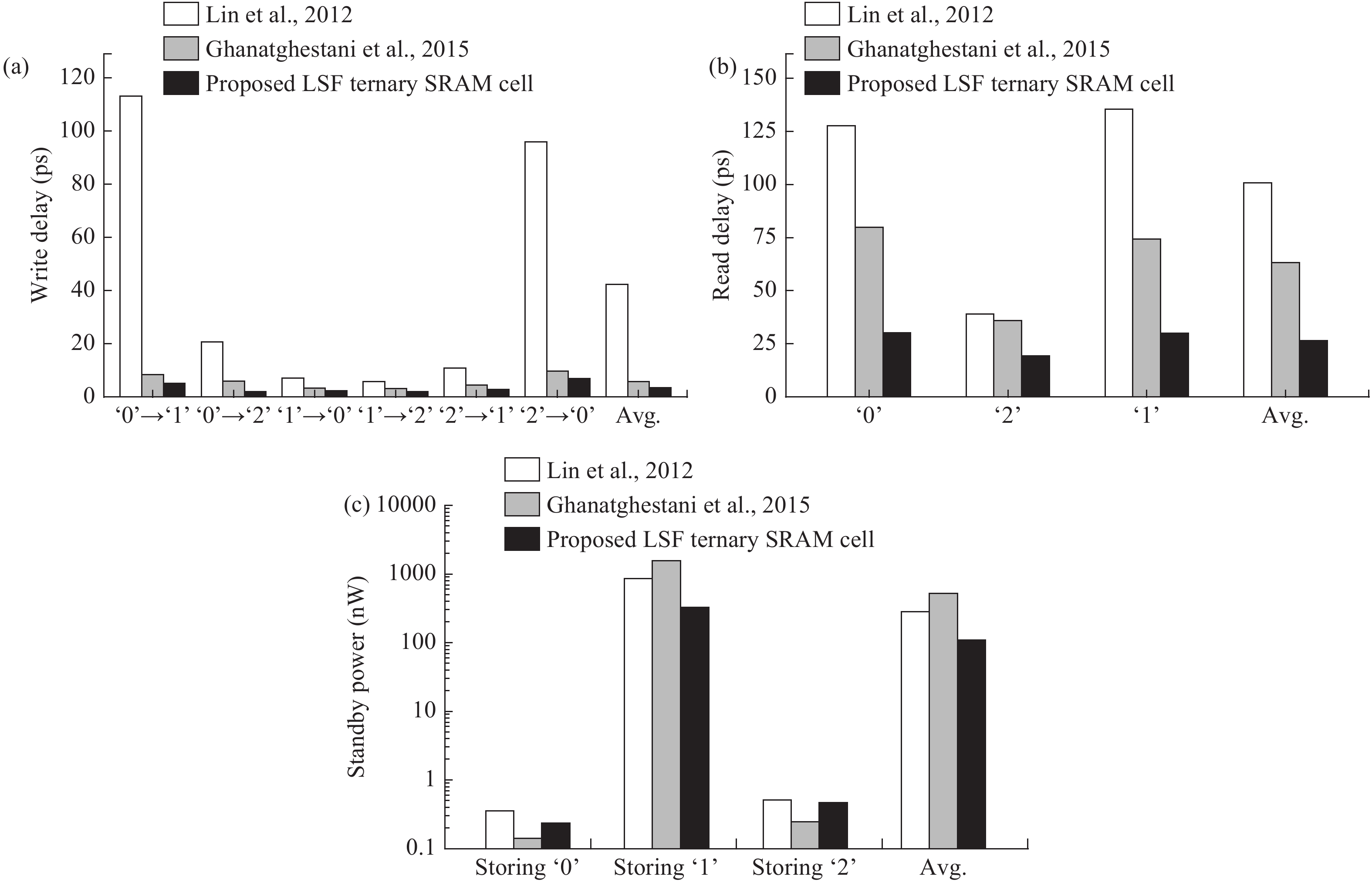
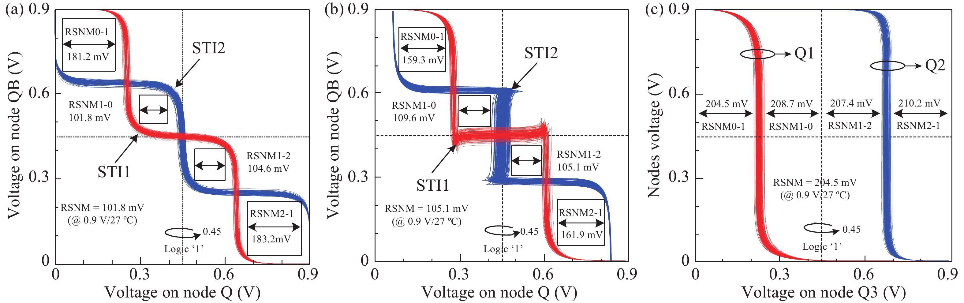
Table 1. Logic symbols and truth table of the 1T-2B and 2B-1T.
| Logic symbol | 1T-2B | 2B-1T | |||||||
| Ternary | Binary | Binary | Ternary | ||||||
| Voltage level (V) | Logic level | Q3 | Q1 | Q2 | Q1 | Q2 | Q3 | ||
| 0 | 0 | 0 | 2 | 2 | 2 | 2 | 0 | ||
| 0.45 | 1 | 1 | 0 | 2 | 0 | 2 | 1 | ||
| 0.9 | 2 | 2 | 0 | 0 | 0 | 0 | 2 | ||
 DownLoad: CSV
Table 2. The important device parameters of the CNFET model.
| Parameter | Value | |
| Physical channel length | 32 nm | |
| Mean free path in the intrinsic CNT | 100 nm | |
| Length of doped CNT drain-side region | 32 nm | |
| Length of doped CNT source-side region | 32 nm | |
| Mean free path in p+/n+ doped CNT | 15 nm | |
| Distance between the lefts of two adjacent CNTs within the same gate | ≤ 30 nm | |
| Sub-lithographic pitch | 4 nm | |
| Thickness of high-k top gate dielectric | 4 nm | |
| Dielectric constant of high-k top gate dielectric material (HfO2) | 16 | |
| Dielectric constant of substrate (SiO2) | 4 | |
| Coupling cap between the channel region and the substrate (SiO2) | 40 aF/μm | |
| Fermi level of the doped S/D CNT | 6 eV | |
| Work function of S/D metal contacts | 4.6 eV | |
| CNT work function | 4.5 eV |
DownLoad: CSV
Table 3. Simulation results and comparisons with other related works.
| Parameter | Ref. [14] | Ref. [2] | Ref. [8] | Ref. [9] | Proposed | ||
| Technology (nm) | CMOS 120 | CMOS 180 | CNFET 32 | CNFET 32 | CNFET 32 | ||
| Logic type | Binary | Binary | Ternary | Ternary | Ternary | Ternary | |
| Supply voltage (V) | 1.2 | 1.2 | 1.8 | 0.9 | 0.9 | 0.9 | |
| Number of transistors | 6 | 11 | 10 | 18 | 18 | 18 | |
| Write delay (ps) | ‘0’→‘1’ | × | × | 840 | 113.10 | 8.49 | 5.19 |
| ‘0’→‘2’ | 111 | 60 | 650 | 20.64 | 5.94 | 2.05 | |
| ‘1’→‘0’ | × | × | 120 | 7.19 | 3.39 | 2.44 | |
| ‘1’→‘2’ | × | × | 570 | 5.85 | 3.14 | 1.99 | |
| ‘2’→‘0’ | 111 | 60 | 160 | 10.90 | 4.54 | 2.78 | |
| ‘2’→‘1’ | × | × | 1230 | 95.91 | 9.82 | 6.89 | |
| Avg. | 111 | 60 | 595 | 42.27 | 5.89 | 3.56 | |
| Read delay (ps) | ‘0’ | 80 | 85 | 200 | 127.60 | 79.75 | 30.20 |
| ‘1’ | × | × | 3900 | 39.00 | 35.85 | 19.38 | |
| ‘2’ | 80 | 14 | 165 | 135.30 | 74.25 | 30.10 | |
| Avg. | 80 | 49.5 | 14 212 | 100.63 | 63.28 | 26.44 | |
| Standby-power (nW) | ‘0’ | N/A | N/A | N/A | 0.3515 | 0.1359 | 0.2334 |
| ‘1’ | N/A | N/A | N/A | 828.7 | 1495.5 | 326.9 | |
| ‘2’ | N/A | N/A | N/A | 0.5104 | 0.2425 | 0.4538 | |
| Avg. | N/A | N/A | N/A | 276.5 | 498.6 | 109.2 | |
| RSNM (mV) | 195* | 395* | N/A | 101.8 | 105.1 | 204.5 | |
| Read-disturb problem | Yes | No | Yes | No | Yes | No | |
| Half-select problem | Yes | Yes | Yes | Yes | Yes | No | |
| ×−Not exist; N/A−Not available; * Simulated without process variations. | |||||||
DownLoad: CSV
| [1] |
Cho G, Lombardi F. Design and process variation analysis of CNTFET-based ternary memory cells. Integr VLSI J, 2011, 54(C): 97
|
| [2] |
Kamar Z, Nepal K. Noise margin-optimized ternary CMOS SRAM delay and sizing characteristics. IEEE International Midwest Symposium on Circuits and Systems (MWSCAS), 2010: 801
|
| [3] |
Zhang Y J, Wang P J, Xiong B Y, et al. Design of a high information-density multiple valued 2-read 1-write register file. IEICE Electron Express, 2012, 9(11): 958 doi: 10.1587/elex.9.958
|
| [4] |
Appenzeller J. Carbon nanotubes for high-performance electronics—progress and prospect. Proc IEEE, 2008, 96(2): 201 doi: 10.1109/JPROC.2007.911051
|
| [5] |
Lin Y M, Appenzeller J, Knoch J, et al. High performance carbon nanotube field-effect transistor with tunable polarities. IEEE Trans Nanotechnol, 2005, 4(5): 481 doi: 10.1109/TNANO.2005.851427
|
| [6] |
Qiu C, Zhang Z, Xiao M, et al. Scaling carbon nanotube complementary transistors to 5-nm gate lengths. Science, 2017, 355(6322): 271 doi: 10.1126/science.aaj1628
|
| [7] |
You K, Nepal K. Design of a ternary static memory cell using carbon nanotube-based transistors. IET Micro & Nano Lett, 2011, 6(6): 381
|
| [8] |
Lin S, Kim Y B, Lombardi F. Design of a ternary memory cell using CNTFETs. IEEE Trans Nanotechnol, 2012, 11(5): 1019 doi: 10.1109/TNANO.2012.2211614
|
| [9] |
Ghanatghestani M M, Pedram H, Ghavami B. Design of a low-standby power and high-speed ternary memory cell based on carbon nanotube field-effect transistor. J Comput Theor Nanosci, 2015, 12(12): 5457 doi: 10.1166/jctn.2015.4546
|
| [10] |
Ebrahim A, Abdolreza D. A novel design of low power and high read stability ternary SRAM (T-SRAM), memory based on the modified gate diffusion input (m-GDI) method in nanotechnology. Microelectron J, 2016, 58: 44 doi: 10.1016/j.mejo.2016.10.009
|
| [11] |
Shin K, Choi W, Park J. Half-select free and bit-line sharing 9T SRAM for reliable supply voltage scaling. IEEE Trans Circ Syst I, 2017, 64(8): 2036
|
| [12] |
Deng J, Wong H S P. A compact SPICE model for carbon-nanotube field effect transistors including nonidealities and its application-part II: model of the intrinsic channel region. IEEE Trans Electron Devices, 2007, 54(12): 3186 doi: 10.1109/TED.2007.909030
|
| [13] |
Tabrizchi S, Azimi N, Navi K. A novel ternary half adder and multiplier based on carbon nanotube field effect transistors. Front Inform Technol Electron Eng, 2017, 18(3): 423 doi: 10.1631/FITEE.1500366
|
| [14] |
Prabhu C M R, Singh A K. Low-power fast (LPF) SRAM cell for write/read operation. IEICE Electron Express, 2011, 8(18): 1473 doi: 10.1587/elex.8.1473
|


Article views: 5082 Times PDF downloads: 104 Times Cited by: 0 Times
Received: 15 November 2017 Revised: 06 February 2018 Online: Uncorrected proof: 20 April 2018Accepted Manuscript: 23 April 2018Published: 09 August 2018
| Citation: |
Gang Li, Pengjun Wang, Yaopeng Kang, Yuejun Zhang. A low standby-power fast carbon nanotube ternary SRAM cell with improved stability[J]. Journal of Semiconductors, 2018, 39(8): 085002. doi: 10.1088/1674-4926/39/8/085002
****
G Li, P J Wang, Y P Kang, Y J Zhang, A low standby-power fast carbon nanotube ternary SRAM cell with improved stability[J]. J. Semicond., 2018, 39(8): 085002. doi: 10.1088/1674-4926/39/8/085002.

|
| [1] |
Cho G, Lombardi F. Design and process variation analysis of CNTFET-based ternary memory cells. Integr VLSI J, 2011, 54(C): 97
|
| [2] |
Kamar Z, Nepal K. Noise margin-optimized ternary CMOS SRAM delay and sizing characteristics. IEEE International Midwest Symposium on Circuits and Systems (MWSCAS), 2010: 801
|
| [3] |
Zhang Y J, Wang P J, Xiong B Y, et al. Design of a high information-density multiple valued 2-read 1-write register file. IEICE Electron Express, 2012, 9(11): 958 doi: 10.1587/elex.9.958
|
| [4] |
Appenzeller J. Carbon nanotubes for high-performance electronics—progress and prospect. Proc IEEE, 2008, 96(2): 201 doi: 10.1109/JPROC.2007.911051
|
| [5] |
Lin Y M, Appenzeller J, Knoch J, et al. High performance carbon nanotube field-effect transistor with tunable polarities. IEEE Trans Nanotechnol, 2005, 4(5): 481 doi: 10.1109/TNANO.2005.851427
|
| [6] |
Qiu C, Zhang Z, Xiao M, et al. Scaling carbon nanotube complementary transistors to 5-nm gate lengths. Science, 2017, 355(6322): 271 doi: 10.1126/science.aaj1628
|
| [7] |
You K, Nepal K. Design of a ternary static memory cell using carbon nanotube-based transistors. IET Micro & Nano Lett, 2011, 6(6): 381
|
| [8] |
Lin S, Kim Y B, Lombardi F. Design of a ternary memory cell using CNTFETs. IEEE Trans Nanotechnol, 2012, 11(5): 1019 doi: 10.1109/TNANO.2012.2211614
|
| [9] |
Ghanatghestani M M, Pedram H, Ghavami B. Design of a low-standby power and high-speed ternary memory cell based on carbon nanotube field-effect transistor. J Comput Theor Nanosci, 2015, 12(12): 5457 doi: 10.1166/jctn.2015.4546
|
| [10] |
Ebrahim A, Abdolreza D. A novel design of low power and high read stability ternary SRAM (T-SRAM), memory based on the modified gate diffusion input (m-GDI) method in nanotechnology. Microelectron J, 2016, 58: 44 doi: 10.1016/j.mejo.2016.10.009
|
| [11] |
Shin K, Choi W, Park J. Half-select free and bit-line sharing 9T SRAM for reliable supply voltage scaling. IEEE Trans Circ Syst I, 2017, 64(8): 2036
|
| [12] |
Deng J, Wong H S P. A compact SPICE model for carbon-nanotube field effect transistors including nonidealities and its application-part II: model of the intrinsic channel region. IEEE Trans Electron Devices, 2007, 54(12): 3186 doi: 10.1109/TED.2007.909030
|
| [13] |
Tabrizchi S, Azimi N, Navi K. A novel ternary half adder and multiplier based on carbon nanotube field effect transistors. Front Inform Technol Electron Eng, 2017, 18(3): 423 doi: 10.1631/FITEE.1500366
|
| [14] |
Prabhu C M R, Singh A K. Low-power fast (LPF) SRAM cell for write/read operation. IEICE Electron Express, 2011, 8(18): 1473 doi: 10.1587/elex.8.1473
|

 WeChat ID
Journal of Semiconductors © 2017 All Rights Reserved 京ICP备05085259号-2


