


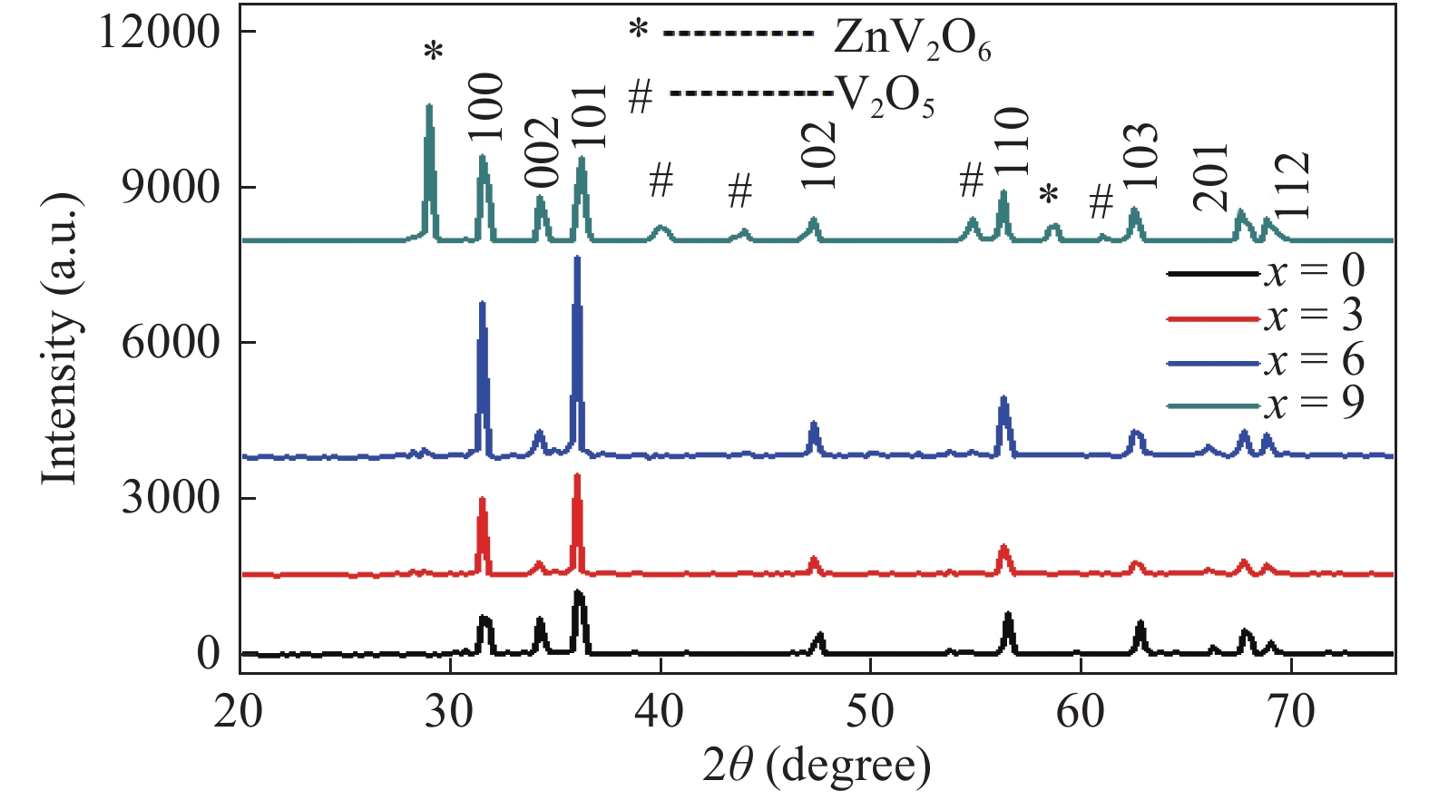
Fig. 1.
(Color online) X-ray diffraction (XRD) patterns of (ZnO)1−x(V2O5)x composite.
SEMICONDUCTOR PHYSICS
Amjid Iqbal, Arshad Mahmood, Q. Raza, A. Shah, Rashad Rashid, Zahid Ali, A. Malik and U. Aziz
Corresponding author: Amjid Iqbal, E-mail address: Amjid821@gmail.com
Abstract: This paper demonstrates the structural, vibrational and photoluminescence characteristics of (ZnO)1−x(V2O5)x (x = 0, 3, 6 and 9 mol%) composites semiconductor synthesized by using the solid state reaction method. X-ray diffraction (XRD) studies show that (ZnO)1−x(V2O5)x composites have the poly crystalline wurtzite structure of hexagonal ZnO. It is found from the XRD results that the lattice constants and the crystallite size increase while the dislocation density decreases with increase in doping concentration. The existence of E1 (TO) and E2 (high) Raman modes show that the ZnO still preserve wurtzite structure after doping vanadium oxide, which is in agreement with XRD results. Room temperature photoluminescence (PL) exhibit near band edge and broad deep level emission while indicating the suppression of deep level emission with the incorporation of V2O5 up to a certain concentration (x < 9). Moreover, the optical band gap increase with doping, which is accompanied by the blue shift of the NBE emission.
Keywords: Raman modes, dislocation density, band edge emission, (ZnO)1−x(V2O5)x, luminescence
| [1] |
Look D C. Recent advances in ZnO materials and devices. Mater Sci Eng B, 2001, 80(1–3): 383 doi: 10.1016/S0921-5107(00)00604-8
|
| [2] |
Lee S Y, Shim E S, Kang H S, et al. Fabrication of ZnO thin film diode using laser annealing. Thin Solid Films, 2005, 473(1): 31 doi: 10.1016/j.tsf.2004.06.194
|
| [3] |
Wang Z L, Kong X Y, Ding Y, et al. Semiconducting and piezoelectric oxide nanostructures induced by polar surface. Adv Funct Mater, 2004, 14: 943 doi: 10.1002/(ISSN)1616-3028
|
| [4] |
Harima H. Raman studies on spintronics materials based on wide band gap semiconductors. J Phys: Conden Matter, 2004, 16: S5653 doi: 10.1088/0953-8984/16/48/023
|
| [5] |
Könenkamp R, Word R C, Schlegel C. Verical nano wire light emitting diode. Appl Phys Lett, 2004, 85(24): 6004 doi: 10.1063/1.1836873
|
| [6] |
Faiz M, Tabet N, Mekki A, et al. X-ray absorption near edge structure investigation of vanadium doped ZnO thin films. Thin Solid Films, 2006, 515(4): 1377 doi: 10.1016/j.tsf.2006.03.044
|
| [7] |
Karamat S, Rawat R S, Lee P, et al. Structural, compositional and magnetic characterization of bulk V2O5 doped ZnO system. Appl Surf Sci, 2010, 256(8): 2309 doi: 10.1016/j.apsusc.2009.09.039
|
| [8] |
Koleva M E, Atanasov P A, Nedialkov N N, et al. Role of vanadium contents in zno thin films grown by pulse laser deposition. Appl Surf Sci, 2007, 254(4): 1228 doi: 10.1016/j.apsusc.2007.07.180
|
| [9] |
Tahir N, Hussain S T, Usman M, et al. Effect of vanadium doping on structural, magnetic and optical properties of ZnO nanoparticle. Appl Surf Sci, 2009, 255(20): 8506 doi: 10.1016/j.apsusc.2009.06.003
|
| [10] |
Slama R, Ghribi F, Houas A, et al. Visible photocatalytic properties of vanadium doped zinc oxide aerogel nanopowder. Thin Solid Films, 2011, 519(17): 5792 doi: 10.1016/j.tsf.2010.12.197
|
| [11] |
Mir L E, El Ghoul J, Alaya S, et al. Synthesis and luminescence properties of vanadium-doped nanosized zinc oxide aerogel. Physica B, 2008, 403(10/11): 1770
|
| [12] |
Mir L E, Ayadi Z B, Saadoun M, et al. Optical, electrical and magnetic properties of transparent, n-type conductive Zn0.90−xV0.10AlxO thin films elaborated from aerogel nanoparticles. Phys Stat Sol, 2007, 204: 3266 doi: 10.1002/pssa.v204:10
|
| [13] |
Wang L, Meng L, Teixeira V, et al. Structural and optical properties of ZnO:V thin films with different doping concentration. Thin Solid Film, 2009, 517(13): 3721 doi: 10.1016/j.tsf.2008.12.043
|
| [14] |
Saeki H, Tobata H, Kawai T. Magnetic and electric properties of vanadium doped ZnO films. Solid State Commun, 2001, 120(11): 439 doi: 10.1016/S0038-1098(01)00400-8
|
| [15] |
Krithiga R, Chandrasekaran G. Synthesis, structural and optical properties of vanadium doped ZnO nanograins. J Cryst Growth, 2011, 311(21): 610
|
| [16] |
Wei L, Zhang L T, Zhang Y, et al. Enhanced ultraviolet photoluminescence from V doped zno thin films by sol gel process. Phys Status Solidi A, 2007, 204(7): 2426 doi: 10.1002/pssa.v204:7
|
| [17] |
Cullity B D, Stock S R. Elements of X-ray diffraction. 3rd ed. Addison Wesley Publishing Company, Inc., USA, 2001
|
| [18] |
Rickerby D S, Jones A M, Bellamy B A. X-ray diffraction studies of physically vapour-deposited coatings. Surf Coat Technol, 1989, 37(1): 111 doi: 10.1016/0257-8972(89)90124-2
|
| [19] |
Chikoidze E, Dumont Y, Omard F J, et al. ZnO:Mn as a member II–VI:Mn family. Appl Phy A, 2007, 88(1): 167 doi: 10.1007/s00339-007-3947-3
|
| [20] |
Cullity B D. Elements of X-ray diffraction. 2nd ed. Addison Wesley, 1978: 102
|
| [21] |
Williamson G K, Smallman R E. Dislocation densities in some annealed and cold-worked metals from measurements on the X-ray debye-scherrer spectrum. Phil Mag, 1956, 1(1): 34 doi: 10.1080/14786435608238074
|
| [22] |
Damen T C, Porto S P S, Tells B. Raman effect in ZnO. Phys Rev, 1966, 142(2): 570 doi: 10.1103/PhysRev.142.570
|
| [23] |
Lasser M L G. Symmetry properties of the wurtzite structure. J Phys Chem Solid, 1959, 10(2/3): 229
|
| [24] |
Sudakar C, Kharel P, Lawes G, et al. Raman spectroscopic studies of oxygen defects in Co doped ZnO thin films exhibiting room temperature ferromagnetisim. J Phys Condens Matter, 2007, 19(2): 026212 doi: 10.1088/0953-8984/19/2/026212
|
| [25] |
Maslar J E, Hurst W S, Vanderah T A, et al. The Raman spectra of Cr3O8 and Cr2O5. J Raman Spectrosc, 2001, 32(3): 201 doi: 10.1002/(ISSN)1097-4555
|
| [26] |
Joshi R, Kumar P, Gaur A, et al. Structural, optical and ferroelectric properties of V doped ZnO. Appl Nanosci, 2014, 4(5): 531 doi: 10.1007/s13204-013-0231-z
|
| [27] |
Khan T M, Irfan M. Studies on the complex behaviour of optical phonon modes in wurtzite (ZnO)1−x(Cr2O3)x. Appl Phys A, 2014, 117(3): 1275 doi: 10.1007/s00339-014-8518-9
|
| [28] |
Wang X J, Li H D, Fei Y J, et al. XRD and Raman study of vanadium oxide thin films deposited on fused silica by RF magnetron sputtering. Appl Surf Sci, 2001, 177(1/2): 8
|
| [29] |
Chen W, Mai L, Peng J, et al. Raman spectroscopic study of vanadium oxide nanotubes. J Solid State Chem, 2004, 177(1): 377 doi: 10.1016/S0022-4596(03)00416-X
|
| [30] |
Shan F K, Kim B I, Liu G X, et al. Blue shift of near band edge emission in Mg doped ZnO thin films and aging. J Appl Phys, 2004, 95(9): 4772 doi: 10.1063/1.1690091
|
| [31] |
Burstein E. Anomalous optical absorption limit in InSb. Phys Rev, 1954, 93(3): 632 doi: 10.1103/PhysRev.93.632
|
| [32] |
Tsang J C, Dean P J, Landsberg P T. Concentration quenching of luminescence by donar or acceptor in GaP and impurity band auger model. Phys Rev, 1968, 173(3): 814 doi: 10.1103/PhysRev.173.814
|
| [33] |
Dingle R. Luminescent transition associated with divalent impurities and green emission from semiconducting ZnO. Phys Rev Lett, 1969, 23(11): 579 doi: 10.1103/PhysRevLett.23.579
|
| [34] |
Studenikin S A, Cocivera M. Time resolved luminescence and photoconductivity of poly crystalline ZnO films. J Appl Phy, 2002, 91(8): 5060 doi: 10.1063/1.1461890
|
| [35] |
Shan F K, Shin B C, Kim S C, et al. Optical property and aging effect of ZnO thin films. J Kor Phys Soc, 2003, 42(31): 1174
|
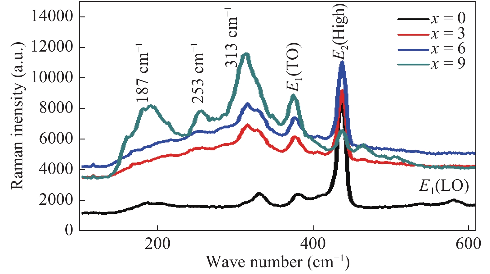
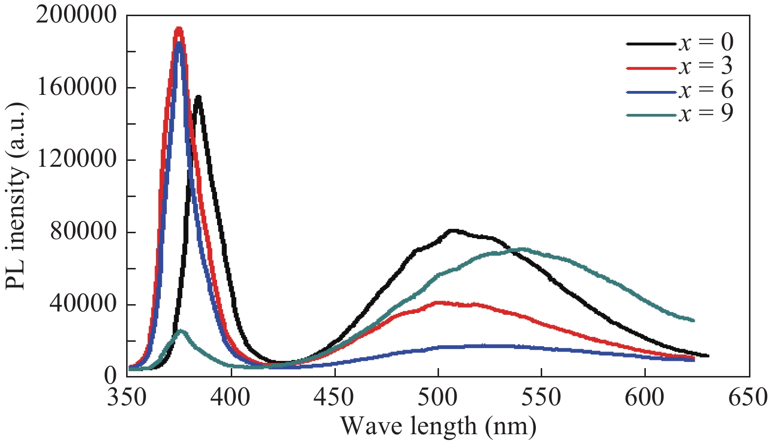
Table 1. Lattice parameters for different samples.
| S. No | V2O5 composition
(mol%) |
Lattice constant c
(nm) |
Lattice constant a
(nm) |
Grain size
(nm) |
Dislocation density
δ (10−3 nm−2) |
| 1 | 0 | 0.5219822 | 0.3262389 | 24.8756 | 1.6 |
| 2 | 3 | 0.5230075 | 0.3268797 | 26.15097 | 1.4 |
| 3 | 6 | 0.5249813 | 0.3281133 | 31.2996 | 1.021 |
| 4 | 9 | 0.523047 | 0.3269044 | 22.2252 | 2.024 |
 DownLoad: CSV
| [1] |
Look D C. Recent advances in ZnO materials and devices. Mater Sci Eng B, 2001, 80(1–3): 383 doi: 10.1016/S0921-5107(00)00604-8
|
| [2] |
Lee S Y, Shim E S, Kang H S, et al. Fabrication of ZnO thin film diode using laser annealing. Thin Solid Films, 2005, 473(1): 31 doi: 10.1016/j.tsf.2004.06.194
|
| [3] |
Wang Z L, Kong X Y, Ding Y, et al. Semiconducting and piezoelectric oxide nanostructures induced by polar surface. Adv Funct Mater, 2004, 14: 943 doi: 10.1002/(ISSN)1616-3028
|
| [4] |
Harima H. Raman studies on spintronics materials based on wide band gap semiconductors. J Phys: Conden Matter, 2004, 16: S5653 doi: 10.1088/0953-8984/16/48/023
|
| [5] |
Könenkamp R, Word R C, Schlegel C. Verical nano wire light emitting diode. Appl Phys Lett, 2004, 85(24): 6004 doi: 10.1063/1.1836873
|
| [6] |
Faiz M, Tabet N, Mekki A, et al. X-ray absorption near edge structure investigation of vanadium doped ZnO thin films. Thin Solid Films, 2006, 515(4): 1377 doi: 10.1016/j.tsf.2006.03.044
|
| [7] |
Karamat S, Rawat R S, Lee P, et al. Structural, compositional and magnetic characterization of bulk V2O5 doped ZnO system. Appl Surf Sci, 2010, 256(8): 2309 doi: 10.1016/j.apsusc.2009.09.039
|
| [8] |
Koleva M E, Atanasov P A, Nedialkov N N, et al. Role of vanadium contents in zno thin films grown by pulse laser deposition. Appl Surf Sci, 2007, 254(4): 1228 doi: 10.1016/j.apsusc.2007.07.180
|
| [9] |
Tahir N, Hussain S T, Usman M, et al. Effect of vanadium doping on structural, magnetic and optical properties of ZnO nanoparticle. Appl Surf Sci, 2009, 255(20): 8506 doi: 10.1016/j.apsusc.2009.06.003
|
| [10] |
Slama R, Ghribi F, Houas A, et al. Visible photocatalytic properties of vanadium doped zinc oxide aerogel nanopowder. Thin Solid Films, 2011, 519(17): 5792 doi: 10.1016/j.tsf.2010.12.197
|
| [11] |
Mir L E, El Ghoul J, Alaya S, et al. Synthesis and luminescence properties of vanadium-doped nanosized zinc oxide aerogel. Physica B, 2008, 403(10/11): 1770
|
| [12] |
Mir L E, Ayadi Z B, Saadoun M, et al. Optical, electrical and magnetic properties of transparent, n-type conductive Zn0.90−xV0.10AlxO thin films elaborated from aerogel nanoparticles. Phys Stat Sol, 2007, 204: 3266 doi: 10.1002/pssa.v204:10
|
| [13] |
Wang L, Meng L, Teixeira V, et al. Structural and optical properties of ZnO:V thin films with different doping concentration. Thin Solid Film, 2009, 517(13): 3721 doi: 10.1016/j.tsf.2008.12.043
|
| [14] |
Saeki H, Tobata H, Kawai T. Magnetic and electric properties of vanadium doped ZnO films. Solid State Commun, 2001, 120(11): 439 doi: 10.1016/S0038-1098(01)00400-8
|
| [15] |
Krithiga R, Chandrasekaran G. Synthesis, structural and optical properties of vanadium doped ZnO nanograins. J Cryst Growth, 2011, 311(21): 610
|
| [16] |
Wei L, Zhang L T, Zhang Y, et al. Enhanced ultraviolet photoluminescence from V doped zno thin films by sol gel process. Phys Status Solidi A, 2007, 204(7): 2426 doi: 10.1002/pssa.v204:7
|
| [17] |
Cullity B D, Stock S R. Elements of X-ray diffraction. 3rd ed. Addison Wesley Publishing Company, Inc., USA, 2001
|
| [18] |
Rickerby D S, Jones A M, Bellamy B A. X-ray diffraction studies of physically vapour-deposited coatings. Surf Coat Technol, 1989, 37(1): 111 doi: 10.1016/0257-8972(89)90124-2
|
| [19] |
Chikoidze E, Dumont Y, Omard F J, et al. ZnO:Mn as a member II–VI:Mn family. Appl Phy A, 2007, 88(1): 167 doi: 10.1007/s00339-007-3947-3
|
| [20] |
Cullity B D. Elements of X-ray diffraction. 2nd ed. Addison Wesley, 1978: 102
|
| [21] |
Williamson G K, Smallman R E. Dislocation densities in some annealed and cold-worked metals from measurements on the X-ray debye-scherrer spectrum. Phil Mag, 1956, 1(1): 34 doi: 10.1080/14786435608238074
|
| [22] |
Damen T C, Porto S P S, Tells B. Raman effect in ZnO. Phys Rev, 1966, 142(2): 570 doi: 10.1103/PhysRev.142.570
|
| [23] |
Lasser M L G. Symmetry properties of the wurtzite structure. J Phys Chem Solid, 1959, 10(2/3): 229
|
| [24] |
Sudakar C, Kharel P, Lawes G, et al. Raman spectroscopic studies of oxygen defects in Co doped ZnO thin films exhibiting room temperature ferromagnetisim. J Phys Condens Matter, 2007, 19(2): 026212 doi: 10.1088/0953-8984/19/2/026212
|
| [25] |
Maslar J E, Hurst W S, Vanderah T A, et al. The Raman spectra of Cr3O8 and Cr2O5. J Raman Spectrosc, 2001, 32(3): 201 doi: 10.1002/(ISSN)1097-4555
|
| [26] |
Joshi R, Kumar P, Gaur A, et al. Structural, optical and ferroelectric properties of V doped ZnO. Appl Nanosci, 2014, 4(5): 531 doi: 10.1007/s13204-013-0231-z
|
| [27] |
Khan T M, Irfan M. Studies on the complex behaviour of optical phonon modes in wurtzite (ZnO)1−x(Cr2O3)x. Appl Phys A, 2014, 117(3): 1275 doi: 10.1007/s00339-014-8518-9
|
| [28] |
Wang X J, Li H D, Fei Y J, et al. XRD and Raman study of vanadium oxide thin films deposited on fused silica by RF magnetron sputtering. Appl Surf Sci, 2001, 177(1/2): 8
|
| [29] |
Chen W, Mai L, Peng J, et al. Raman spectroscopic study of vanadium oxide nanotubes. J Solid State Chem, 2004, 177(1): 377 doi: 10.1016/S0022-4596(03)00416-X
|
| [30] |
Shan F K, Kim B I, Liu G X, et al. Blue shift of near band edge emission in Mg doped ZnO thin films and aging. J Appl Phys, 2004, 95(9): 4772 doi: 10.1063/1.1690091
|
| [31] |
Burstein E. Anomalous optical absorption limit in InSb. Phys Rev, 1954, 93(3): 632 doi: 10.1103/PhysRev.93.632
|
| [32] |
Tsang J C, Dean P J, Landsberg P T. Concentration quenching of luminescence by donar or acceptor in GaP and impurity band auger model. Phys Rev, 1968, 173(3): 814 doi: 10.1103/PhysRev.173.814
|
| [33] |
Dingle R. Luminescent transition associated with divalent impurities and green emission from semiconducting ZnO. Phys Rev Lett, 1969, 23(11): 579 doi: 10.1103/PhysRevLett.23.579
|
| [34] |
Studenikin S A, Cocivera M. Time resolved luminescence and photoconductivity of poly crystalline ZnO films. J Appl Phy, 2002, 91(8): 5060 doi: 10.1063/1.1461890
|
| [35] |
Shan F K, Shin B C, Kim S C, et al. Optical property and aging effect of ZnO thin films. J Kor Phys Soc, 2003, 42(31): 1174
|


Article views: 4872 Times PDF downloads: 66 Times Cited by: 0 Times
Received: 30 October 2017 Revised: 12 January 2018 Online: Uncorrected proof: 17 April 2018Accepted Manuscript: 23 April 2018Published: 09 August 2018
| Citation: |
Amjid Iqbal, Arshad Mahmood, Q. Raza, A. Shah, Rashad Rashid, Zahid Ali, A. Malik, U. Aziz. Photoluminescence and structural analysis of wurtzite (ZnO)1−x(V2O5)x composite[J]. Journal of Semiconductors, 2018, 39(8): 082002. doi: 10.1088/1674-4926/39/8/082002
****
A Iqbal, A Mahmood, Q. Raza, A Shah, R Rashid, Z Ali, A Malik, U Aziz, Photoluminescence and structural analysis of wurtzite (ZnO)1−x(V2O5)x composite[J]. J. Semicond., 2018, 39(8): 082002. doi: 10.1088/1674-4926/39/8/082002.

|
| [1] |
Look D C. Recent advances in ZnO materials and devices. Mater Sci Eng B, 2001, 80(1–3): 383 doi: 10.1016/S0921-5107(00)00604-8
|
| [2] |
Lee S Y, Shim E S, Kang H S, et al. Fabrication of ZnO thin film diode using laser annealing. Thin Solid Films, 2005, 473(1): 31 doi: 10.1016/j.tsf.2004.06.194
|
| [3] |
Wang Z L, Kong X Y, Ding Y, et al. Semiconducting and piezoelectric oxide nanostructures induced by polar surface. Adv Funct Mater, 2004, 14: 943 doi: 10.1002/(ISSN)1616-3028
|
| [4] |
Harima H. Raman studies on spintronics materials based on wide band gap semiconductors. J Phys: Conden Matter, 2004, 16: S5653 doi: 10.1088/0953-8984/16/48/023
|
| [5] |
Könenkamp R, Word R C, Schlegel C. Verical nano wire light emitting diode. Appl Phys Lett, 2004, 85(24): 6004 doi: 10.1063/1.1836873
|
| [6] |
Faiz M, Tabet N, Mekki A, et al. X-ray absorption near edge structure investigation of vanadium doped ZnO thin films. Thin Solid Films, 2006, 515(4): 1377 doi: 10.1016/j.tsf.2006.03.044
|
| [7] |
Karamat S, Rawat R S, Lee P, et al. Structural, compositional and magnetic characterization of bulk V2O5 doped ZnO system. Appl Surf Sci, 2010, 256(8): 2309 doi: 10.1016/j.apsusc.2009.09.039
|
| [8] |
Koleva M E, Atanasov P A, Nedialkov N N, et al. Role of vanadium contents in zno thin films grown by pulse laser deposition. Appl Surf Sci, 2007, 254(4): 1228 doi: 10.1016/j.apsusc.2007.07.180
|
| [9] |
Tahir N, Hussain S T, Usman M, et al. Effect of vanadium doping on structural, magnetic and optical properties of ZnO nanoparticle. Appl Surf Sci, 2009, 255(20): 8506 doi: 10.1016/j.apsusc.2009.06.003
|
| [10] |
Slama R, Ghribi F, Houas A, et al. Visible photocatalytic properties of vanadium doped zinc oxide aerogel nanopowder. Thin Solid Films, 2011, 519(17): 5792 doi: 10.1016/j.tsf.2010.12.197
|
| [11] |
Mir L E, El Ghoul J, Alaya S, et al. Synthesis and luminescence properties of vanadium-doped nanosized zinc oxide aerogel. Physica B, 2008, 403(10/11): 1770
|
| [12] |
Mir L E, Ayadi Z B, Saadoun M, et al. Optical, electrical and magnetic properties of transparent, n-type conductive Zn0.90−xV0.10AlxO thin films elaborated from aerogel nanoparticles. Phys Stat Sol, 2007, 204: 3266 doi: 10.1002/pssa.v204:10
|
| [13] |
Wang L, Meng L, Teixeira V, et al. Structural and optical properties of ZnO:V thin films with different doping concentration. Thin Solid Film, 2009, 517(13): 3721 doi: 10.1016/j.tsf.2008.12.043
|
| [14] |
Saeki H, Tobata H, Kawai T. Magnetic and electric properties of vanadium doped ZnO films. Solid State Commun, 2001, 120(11): 439 doi: 10.1016/S0038-1098(01)00400-8
|
| [15] |
Krithiga R, Chandrasekaran G. Synthesis, structural and optical properties of vanadium doped ZnO nanograins. J Cryst Growth, 2011, 311(21): 610
|
| [16] |
Wei L, Zhang L T, Zhang Y, et al. Enhanced ultraviolet photoluminescence from V doped zno thin films by sol gel process. Phys Status Solidi A, 2007, 204(7): 2426 doi: 10.1002/pssa.v204:7
|
| [17] |
Cullity B D, Stock S R. Elements of X-ray diffraction. 3rd ed. Addison Wesley Publishing Company, Inc., USA, 2001
|
| [18] |
Rickerby D S, Jones A M, Bellamy B A. X-ray diffraction studies of physically vapour-deposited coatings. Surf Coat Technol, 1989, 37(1): 111 doi: 10.1016/0257-8972(89)90124-2
|
| [19] |
Chikoidze E, Dumont Y, Omard F J, et al. ZnO:Mn as a member II–VI:Mn family. Appl Phy A, 2007, 88(1): 167 doi: 10.1007/s00339-007-3947-3
|
| [20] |
Cullity B D. Elements of X-ray diffraction. 2nd ed. Addison Wesley, 1978: 102
|
| [21] |
Williamson G K, Smallman R E. Dislocation densities in some annealed and cold-worked metals from measurements on the X-ray debye-scherrer spectrum. Phil Mag, 1956, 1(1): 34 doi: 10.1080/14786435608238074
|
| [22] |
Damen T C, Porto S P S, Tells B. Raman effect in ZnO. Phys Rev, 1966, 142(2): 570 doi: 10.1103/PhysRev.142.570
|
| [23] |
Lasser M L G. Symmetry properties of the wurtzite structure. J Phys Chem Solid, 1959, 10(2/3): 229
|
| [24] |
Sudakar C, Kharel P, Lawes G, et al. Raman spectroscopic studies of oxygen defects in Co doped ZnO thin films exhibiting room temperature ferromagnetisim. J Phys Condens Matter, 2007, 19(2): 026212 doi: 10.1088/0953-8984/19/2/026212
|
| [25] |
Maslar J E, Hurst W S, Vanderah T A, et al. The Raman spectra of Cr3O8 and Cr2O5. J Raman Spectrosc, 2001, 32(3): 201 doi: 10.1002/(ISSN)1097-4555
|
| [26] |
Joshi R, Kumar P, Gaur A, et al. Structural, optical and ferroelectric properties of V doped ZnO. Appl Nanosci, 2014, 4(5): 531 doi: 10.1007/s13204-013-0231-z
|
| [27] |
Khan T M, Irfan M. Studies on the complex behaviour of optical phonon modes in wurtzite (ZnO)1−x(Cr2O3)x. Appl Phys A, 2014, 117(3): 1275 doi: 10.1007/s00339-014-8518-9
|
| [28] |
Wang X J, Li H D, Fei Y J, et al. XRD and Raman study of vanadium oxide thin films deposited on fused silica by RF magnetron sputtering. Appl Surf Sci, 2001, 177(1/2): 8
|
| [29] |
Chen W, Mai L, Peng J, et al. Raman spectroscopic study of vanadium oxide nanotubes. J Solid State Chem, 2004, 177(1): 377 doi: 10.1016/S0022-4596(03)00416-X
|
| [30] |
Shan F K, Kim B I, Liu G X, et al. Blue shift of near band edge emission in Mg doped ZnO thin films and aging. J Appl Phys, 2004, 95(9): 4772 doi: 10.1063/1.1690091
|
| [31] |
Burstein E. Anomalous optical absorption limit in InSb. Phys Rev, 1954, 93(3): 632 doi: 10.1103/PhysRev.93.632
|
| [32] |
Tsang J C, Dean P J, Landsberg P T. Concentration quenching of luminescence by donar or acceptor in GaP and impurity band auger model. Phys Rev, 1968, 173(3): 814 doi: 10.1103/PhysRev.173.814
|
| [33] |
Dingle R. Luminescent transition associated with divalent impurities and green emission from semiconducting ZnO. Phys Rev Lett, 1969, 23(11): 579 doi: 10.1103/PhysRevLett.23.579
|
| [34] |
Studenikin S A, Cocivera M. Time resolved luminescence and photoconductivity of poly crystalline ZnO films. J Appl Phy, 2002, 91(8): 5060 doi: 10.1063/1.1461890
|
| [35] |
Shan F K, Shin B C, Kim S C, et al. Optical property and aging effect of ZnO thin films. J Kor Phys Soc, 2003, 42(31): 1174
|

 WeChat ID
Journal of Semiconductors © 2017 All Rights Reserved 京ICP备05085259号-2


