Loading [MathJax]/jax/output/HTML-CSS/jax.js
J. Semicond. > 2018, Volume 39 > Issue 8 > 083001

SEMICONDUCTOR MATERIALS

Band structure of monolayer of graphene, silicene and silicon-carbide including a lattice of empty or filled holes

N. Nouri and G. Rashedi

+ Author Affiliations

 Corresponding author: G. Rashedi, E-mail: rashedi@phys.ui.ac.ir

DOI: 10.1088/1674-4926/39/8/083001

PDF

Turn off MathJax

Abstract: We have developed a π -orbital tight-binding Hamiltonian model taking into account the nearest neighbors to study the effect of antidot lattices (two dimensional honeycomb lattice of atoms including holes) on the band structure of silicene and silicon carbide (SiC) sheets. We obtained that the band structure of the silicene antidot superlattice strongly depends on the size of embedded holes, and the band gap of the silicene antidot lattice increases by increasing of holes diameter. The band gap of SiC antidot lattice, except for the lattice of the small unit cell, is independent of the holes diameter and also depends on the distance between holes. We obtained that, the band gap of the SiC antidot lattice is the same as the band gap of the corresponding sheet without hole. Also, the electronic properties of the SiC antidot superlattice occupied either by carbon or by silicon atoms are investigated, numerically. Furthermore, we study the effect of occupation of graphene antidot by Si atoms and vice versa. Also, we have calculated the band structure of graphene and silicene antidot lattice filled by Si + C atoms. Finally, we compute the band structure of the SiC antidot lattice including the holes which are filled by C or by Si atoms. Really, in this paper we have generalized the method of paper[38] about graphene antidot with empty holes to the cases of filled holes by different atoms and also to the case of silicene and silicon carbide antidot lattices.

Key words: tight bindingband structureantidotgraphenesiliceneSiC

Graphene and graphene-like nanostructures such as Si and silicon carbide (SiC) nanostructures have attracted a great deal of attention of both experimentalists and theorists[19] in the current decade. They are attractive subjects because of their potential for applications in electronic and optoelectronic devices, sensors, lasers and photodetector diodes[1012]. Most of these applications are based on low-dimensional systems[10, 11]. It is well-known that, the band structures of silicene, the two-dimensional honeycomb structures of silicon atoms, as in graphene for low energies have a linear dispersion[13]. This property causes high carrier mobility ( 2.57×105 cm2 V−1s−1)[13] which makes silicene a useful material for electronic devices[1316]. But, the band structure of silicene like the band structure of graphene lacks a band gap which is an essential problem for silicene and graphene application in transistors[11, 14, 17, 18]. Thus, creating a controllable gap in silicene helps us to use it in circuits.

Recently, band gap engineering of these nanostructures has become a subject of research in the field of nanoscale electronics. So, many interesting methods have been considered for tuning and controlling the band gap of graphene and graphene-like nanostructures (silicene and SiC sheet) such as reducing the material dimensionality to one-dimensional forms like nanowires, nanoribbons and nanotubes[14, 1933], and adding the different chemical species to the main structure like hydrogenation[10, 3437]. Also, making an array of nanoscale perforations in the two-dimensional sheets (which are called antidot lattices) is another method for controlling the band gap and physical properties of graphene and graphene-like sheets. Earlier studies on antidot lattices have been done by Pedersen on a graphene sheet[38]. Pedersen using the tight-binding model obtained that, antidot lattice structure (lattice of holes) in graphene sheet is an effective way to change graphene from a gapless semimetal to gapped semiconductor structure[38]. Then in many works, effects of the holes diameter, holes geometry, lattice geometry and the separation of the holes on the band structures and band gap of graphene are investigated by DFT or tight-binding methods[3951]. Also fabrication of graphene antidots are proposed by several methods[5256].

In the present work, we use the tight-binding model to investigate the electronic properties of two different honeycomb structures including silicene and SiC antidot lattices as it is done for graphene antidot lattice in Ref. [38]. These antidot lattices are two-dimensional honeycomb sheets with holes arranged along the armchair configuration (armchair antidot lattice). In principle, in this work we compare band structure of silicene and SiC antidot lattices computed by tight-binding with the corresponding results of graphene antidot lattice[38]. Also, using the TB method we numerically study the band structure of SiC antidot lattice occupied either by carbon or by silicon atoms. In addition, we obtain the band gap of graphene antidot filled by silicon atoms and vise versa. Then, we calculate the electronic properties of graphene and silicene antidot lattices occupied by Si + C atoms. Finally, we study the effect of holes diameter and the distance between holes on the band structure of the above-mentioned antidot lattices.

The present paper is organized as follows: in Section 2 we describe the TB theory for the corresponding antidot lattice and in Section 3 we present and discuss our numerical results. Finally, we end with conclusions in Section 4.

In this section, we introduce our method of calculation and structures of our considered antidot lattices. In the case of graphene the π electrons are most interesting. This is because the π electrons are free to move in contrast to the other electrons which participate in covalent bonding and therefore they are strongly localized. So, the π electrons constitute the major contribution to the electrical and the optical properties of graphene. We know that structures of silicene and SiC nanosheets are similar to graphene sheet (two-dimensional hexagonal structure)[14, 57, 58]. So, because of these similar structures by graphene structure we can use the π -orbital tight-binding model in investigation of electronic structures of our antidot lattices as it is successfully applied for computing band structures of graphene antidot lattice in Ref. [38]. Our antidot lattice is constructed by hexagonal unit cells. These unit cells are defined by the notation {L,R} [38] where L refers to the side length of the hexagonal unit cell and R defines the radius of the hole of corresponding antidot lattices. For length scales both L and R are multiplied by lattice constant a of their corresponding sheet.

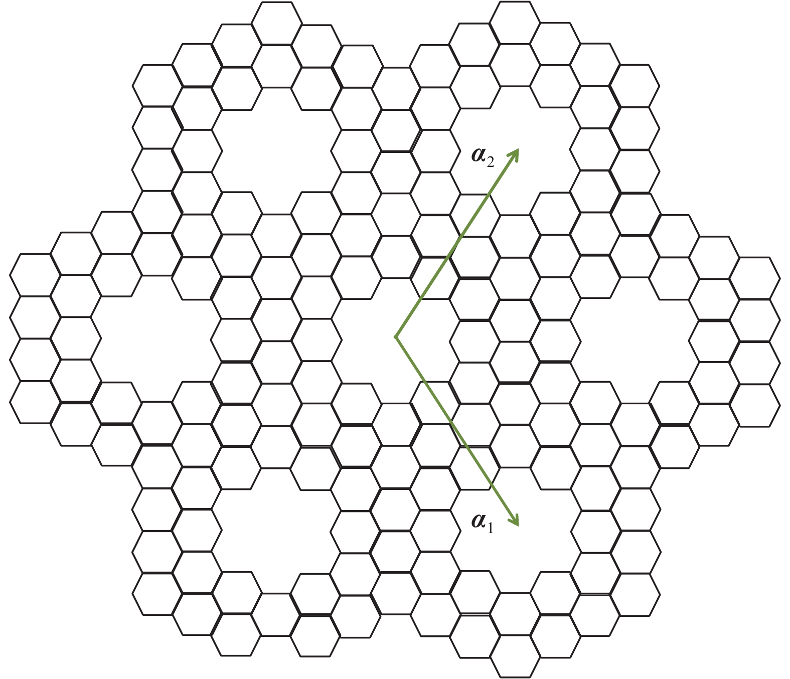
In panels (a, b, c) of Fig. 1 we represent a unit cell of silicene lattice, a unit cell of silicene antidot lattice by empty hole and a unit cell of silicene antidot lattice whose hole is filled by silicon + carbon (Si + C) atoms in direct space, respectively. In our tight-binding calculations we need to know the interaction parameters which can be obtained by experiment or by ab initio calculations. We consider l notation for bond length between two adjacent atoms of antidot lattice (Si–Si, C–C or Si–C), then l=a/3 in which a is lattice constant of graphene-like lattices. The magnitudes of the bond lengths l are 2.22 , 1.42 and 1.77 Å for Si–Si, C–C and Si–C, respectively[14, 59]. In our TB calculations we used these values of bond lengths obtained by DFT calculations for calculating the lattice constant of our proposed antidot lattices. The translation vectors of direct antidot lattice are a1=(La/2)(3,3) and a2=(La/2)(3,3) by length La . In Fig. 2 we show the translation vectors of antidot lattice {3,1} as an example. Also, the basis vectors in the reciprocal lattice are b1=2πLa(13,13) and b2=2πLa(13,13) . It should be noticed that, the Brillouin zone of silicene antidot lattice is the same as graphene antidot lattice because the unit cell of silicene antidot lattice is similar to the case of graphene antidot lattice[38]. Here as in graphene, the wave vectors k of these antidot lattices of silicene and SiC are two dimensional (monolayer). For calculations of the band structure of silicene and SiC antidot lattices, we use a nearest-neighbors ( 1NN ) tight binding model taking into account the π -orbitals. Also as mentioned in Ref. [60] we believed that the effect of relaxation for antidot silicene lattices is not so important and can be neglected. Here, in our calculations as in Ref. [58] we consider a flat monolayer of silicene and silicon carbide without buckling. For this model we write an N×N Hamiltonian for π bonds in which N is the number of atoms in a unit cell of our proposed antidot lattices. We used this model because first-principles calculations have shown that the electronic bands of silicene and SiC sheet near the fermi level are contributed by π -atomic-orbitals[14, 61] as for the case of graphene sheet[62]. So we use this model for describing the band structures of our antidot lattices. Moreover, we used two-center approximation (TCA) in order to obtain the angular dependence of energy integral of π -orbitals[63]. For simplicity we have introduced the parameters which are used in the energy integral in Table 1. Where γ0=(ppπ)1 AB is a term of energy as a hopping integral between nearest neighbor atoms in the unit cell of our antidot lattices and (E)p A(B) refers to on-site energies of π -orbital of A(B) atoms in the corresponding unit cells. Also it is remarkable that as in Refs. [14, 61, 64, 65], the overlap between π -orbitals of atoms in a unit cell can be neglected using a standard approximation for π -electron systems. Also, as in a graphene sheet we define the position vectors of the 1NN for silicene sheets as follows:

Table  1.  Two-center parameters of graphene, silicene and SiC antidot lattices related to π -orbitals of their corresponding sheets.
Parameter Graphene[61] Silicene[14] SiC[60]
(PPπ)IAB −3.033 −0.949 1.42
EAP 0 0 0
EBP 0 0 −2.85
DownLoad: CSV  | Show Table
Figure  1.  (Color online) (a) Hexagonal unit cell of a Si antidot lattice by side length 3 without any hole. Hexagonal unit cell of a Si antidot lattice with notation {3,1} by (b) empty hole and by (c) hole which is filled by silicon + carbon (Si + C) atoms instead of Si atoms. In both cases, the hole is arranged along the armchair direction. Also, the Si and C atoms are shown by blue and red points, respectively. Moreover, we show the border between regions of hole and background of unit cell with orange dash circle in which a is lattice constant.
δ(1)1=(a3,0),δ(1)2=(a23,a2),δ(1)3=(a23,a2). (1)

Then, considering the π bonds, the matrix elements of the corresponding hopping term in the Hamiltonian between A and B atoms of the unit cells are given as:

H(A,B)={γ0eik(rArB),if|rArB|l,0,else, (2)

where rA and rB are the position vectors of A and B atoms in the corresponding unit cells. We have calculated the band structure of above-mentioned antidot lattices taking into account π orbitals. Finally, we compare our numerical results of the 1NN tight binding method in an antidot lattice by empty holes with the corresponding antidot lattice by holes which are filled by other atoms (Si, C or Si + C). Furthermore, using the π -orbital model we investigate the effect of holes diameter and the size of unit cells of graphene, silicene and SiC antidot lattices (by empty holes and by filled holes by different atoms from the background) on the band structure of systems. For instance we study the band structure and band gap of SiC antidot (including holes) whose holes are filled by a two-dimensional array of Si atoms. It should be emphasized that, the physics of our considered antidot lattices are considered from their corresponding sheets by making holes on these sheets and imposing conditions along the holes environment.

We now proceed to study our numerical results obtained from the TB theory.

Here, we present the results of calculations of the band structures of silicene and SiC antidot lattices and the corresponding antidot lattices with filled holes, separately.

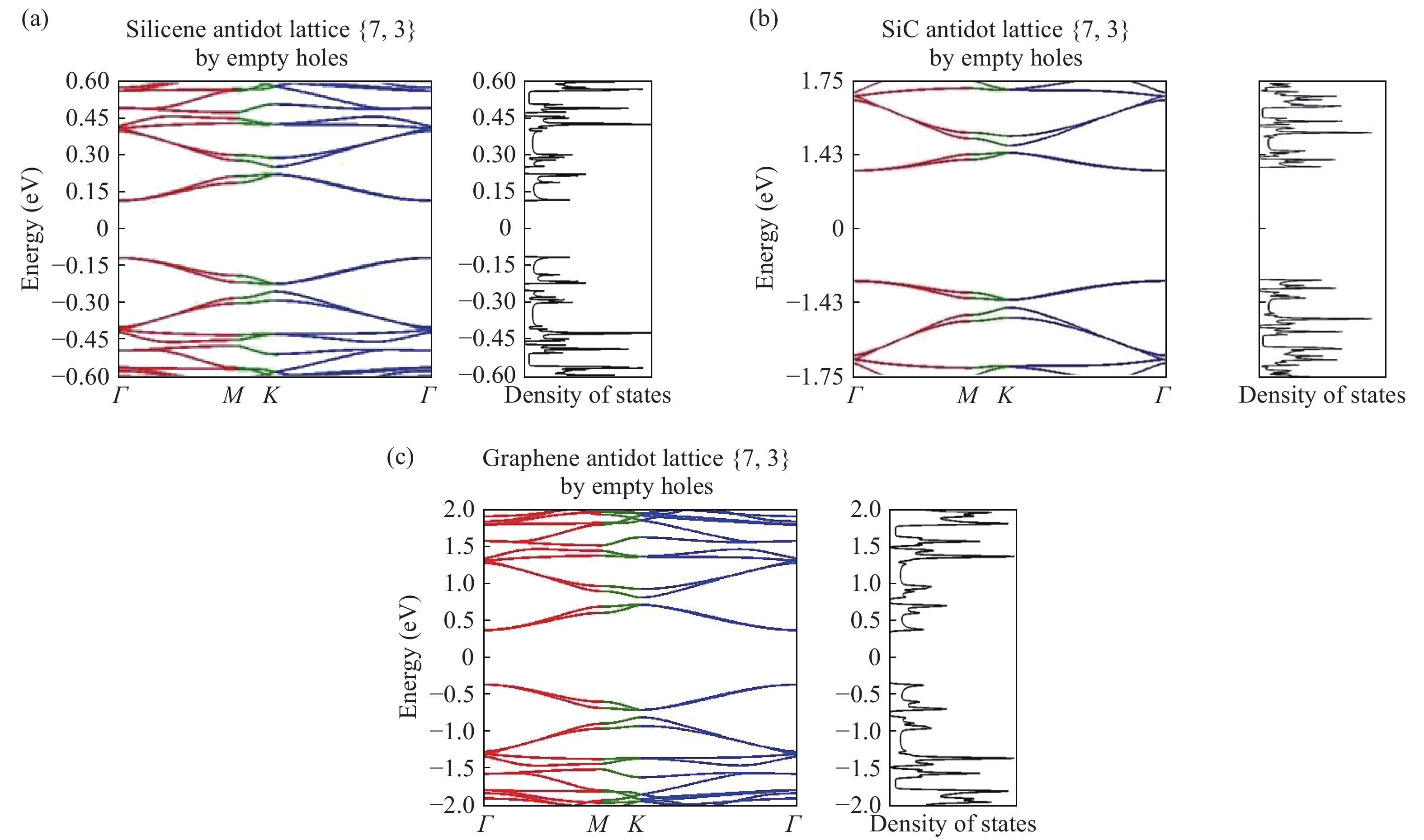
The silicene and SiC antidot lattices which are constructed by making up a triangular array of empty holes on their corresponding two-dimensional sheets, can be specified by a pair of indices {L,R} . The electronic properties of silicene and SiC antidot lattices can be described by the tight-binding approximation. In Fig. 2 we present the triangular antidot lattice {4,1} in which a1 and a2 are translation vectors of the corresponding antidot lattice. By substituting Eq. (2) and the on-site energies mentioned in Table 1 in the N×N Hamiltonian, we obtain the band structure of silicene and SiC antidot lattices using the π -orbital model. Here, N is the number of present atoms in each hexagonal unit cell by length La (a is the lattice constant of background structures) including empty circular hole by radius Ra . In our antidot lattice including N atom we removed Nhole atoms in a circular region by radius Ra from the total number of atoms ( Ntotal ) in the unit cell background. So, by solving our tight binding N×N Hamiltonian we obtain N levels of energy as energy bands. For instance, for the case of the {L,R}={4,1} configuration in Fig. 2, we have 90 levels because the number of present atoms in the antidot lattice is N=90 . In addition, the total number of atoms in the unit cell of the background sheet (without hole) and the number of removed atoms in the circular hole are Ntotal=96 and Nhole=6 , respectively. For example, we have plotted the band structures and their corresponding density of states of the silicene and SiC antidot lattices by indices {7,3} taking into account the π states in Fig. 3(a) and 3(b), respectively. We obtained that, antidot lattices with empty holes of silicene and SiC are semiconductors with a direct band gap the same as the graphene antidot lattices in Ref. [38]. Also in Fig. 3, we obtained a band gap of 0.23 eV for the silicene antidot lattice and 2.86 eV for the SiC antidot lattice with index {7,3} . By comparison of the π energy levels of the silicene antidot lattice with the corresponding ones in the graphene antidot lattice in Fig. 3(c) (also in Ref. [38]), we obtained that the band gap of silicene antidot lattice is about the third part of the corresponding graphene antidot lattice band gap. This difference is because of the differences between the bond length and hopping term for nearest neighbor atoms in silicene and graphene. Also in Figs. 3(a) and 3(c) we see that the forms of band structures of silicene and graphene antidots are similar. This is because silicene and graphene are constructed by the same group atoms of the periodic table (Si and C atoms are in IV group) in a honeycomb structure.

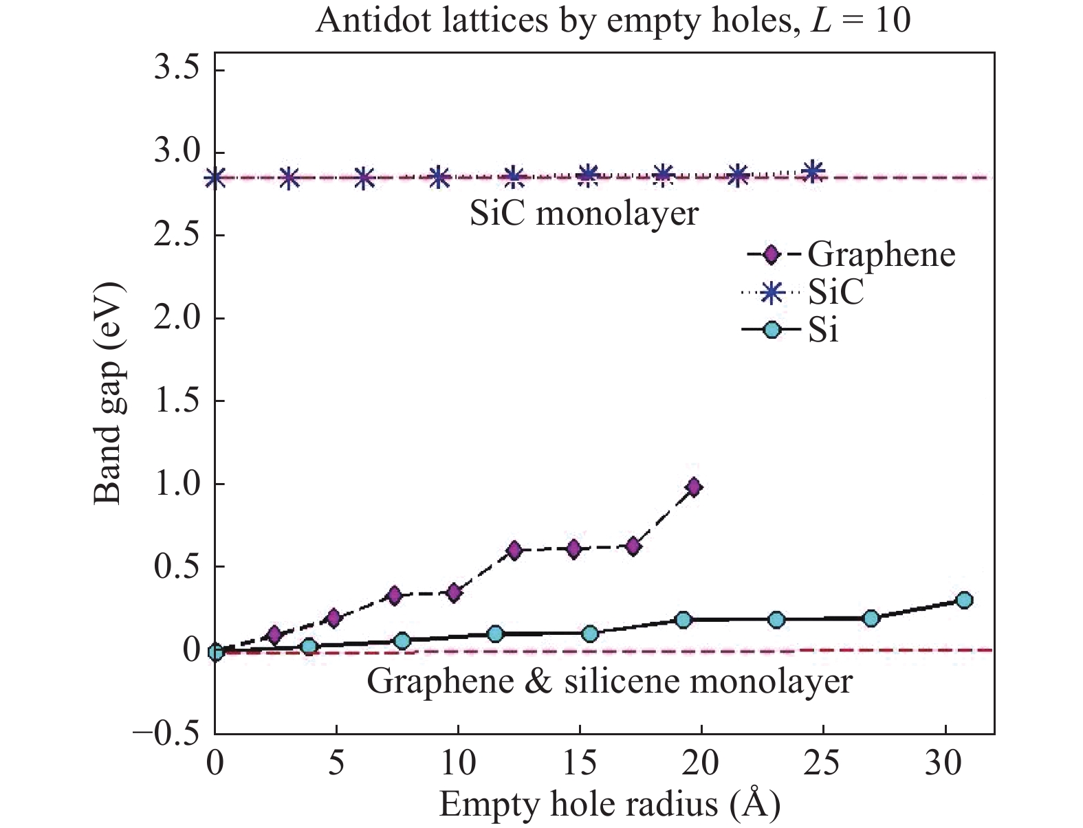
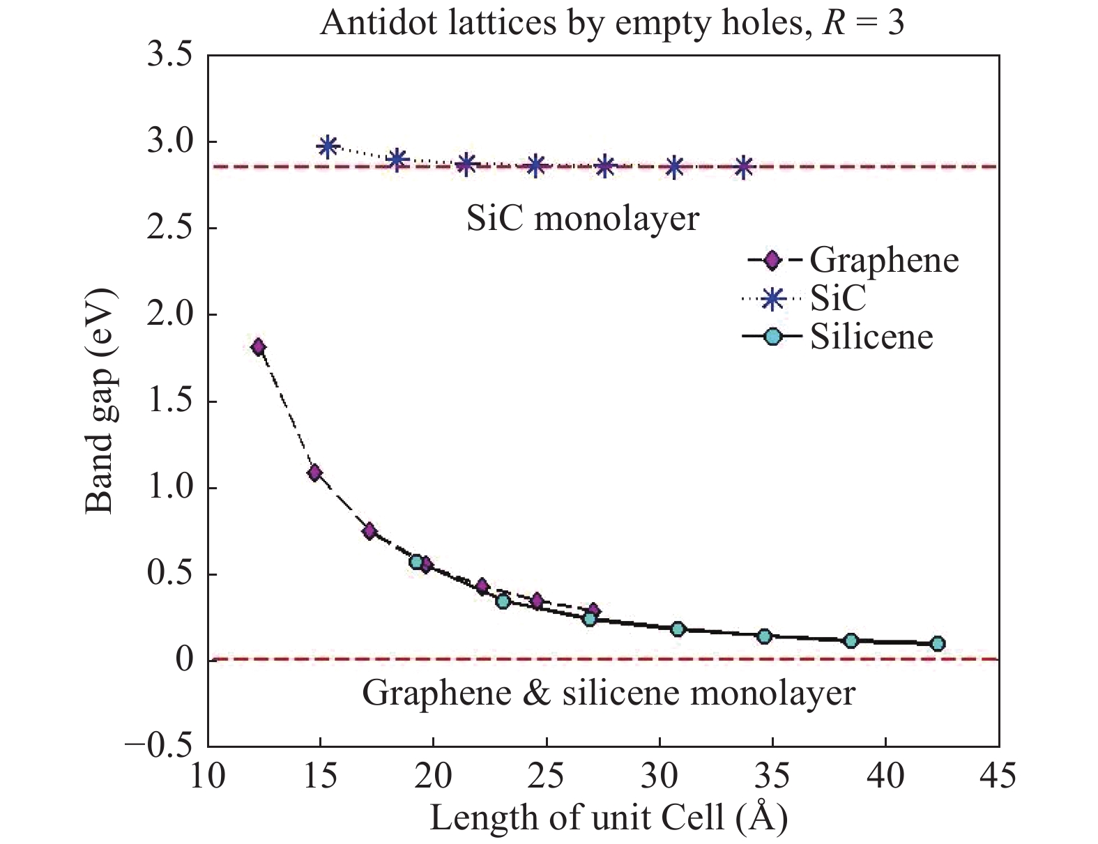
As it is seen in Fig. 3, whereas the creating of holes at the graphene and silicene sheets seriously alters (originates) their corresponding band gap, but the effect of holes on the band gap of SiC sheet is not considerable. We know that, the difference between on-site energies of different atoms in 2D structure causes the band gap, which is absent in the case of graphene sheet or silicene sheet. Thus, for graphene and silicene antidot lattice the main reason for the band gap appearance is the difference between the physics of removed atoms from the hole region and the physics of background atoms. So, we obtain that the band gap of SiC antidot lattice (with holes) is almost equal to the band gap of SiC sheet (without holes). Also in Fig. 4, the hole diameter dependence on the band gaps for graphene, silicene and SiC antidot lattices are investigated. For the silicene antidot lattice, the band gap increases by increasing of the holes diameter as obtained for the case of the graphene antidot lattice in Ref. [38]. While, for the case of SiC antidot lattice, except for the large radius their band gap is almost constant over a wide range of the hole radius. Their band gap coincides with the band gap of the corresponding sheet (2.85 eV). Also, in Fig. 5, the effect of the size of unit cell on the band gap for graphene, silicene and SiC antidot lattices has been investigated. For the silicene antidot lattice, the band gap decreases by increasing the size of unit cell (increasing the distance between holes) as obtained for the case of the graphene antidot lattice in Ref. [38]. In other words, increasing the size of unit cell equals decreasing the density of empty holes and in conclusion decreasing the gap. While, for the case of SiC antidot lattice, except for the small unit cells their band gap is almost constant (equals the band gap of SiC monolayer without hole) over a wide range of the length of unit cell. It should be noticed that simple scaling rule EgκN1/2holeNtotal stated for band gap of graphene antidot lattice with a constant κ=25 eV in Ref. [38] is correct for the band gap of the silicene antidot lattice with a constant κ=8 eV but for the SiC antidot lattice it is not accurate. This scaling rule resulted from the massless Dirac fermion behavior of graphene and silicene sheets close to the K point. We see that, our obtained proportionality constant in the scaling rule of the band gap of silicene antidot lattice ( κ=8 eV) is almost similar to the results of Ref. [60] obtained by DFT calcualtions for silicene antidot including the buckling effect ( κ=7.246 eV). So our results by tight-binding method for a flat silicene antidot lattice look similar to the corresponding results by the DFT method for a buckled silicene antidot lattice. Moreover, our calculated propor- tionality constant for silicene is less than the mentioned proportionality constant in the scaling rule of the band gap of the graphene antidot lattice mentioned in Ref. [38] ( κ=25 eV). That is because the fermi velocity of the massless Dirac fermion of silicene sheet close to the K point (105 m/s)[14] is less than the corresponding one of graphene sheet close to K point (106 m/s)[66, 67]. Here, we try to do an experimental estimate. We know that, applied limitation for lithography of graphene patterns is 10 nm[68, 69]. We consider this lithography limitation for silicene patterns because of the similar structure of silicene and graphene. Thus considering the technological restriction (10 nm limitation for lithography), the maximum number of Si atoms of Ntotal is about 1000 . Assuming Nhole=Ntotal/4 we find a band gap of 0.13 eV using the above-mentioned scaling rule. Band gap of silicene antidot lattices corresponding to lithography limits (0.13 eV) is smaller than the corresponding band gap of graphene antidot lattice (0.23 eV) mentioned in Ref. [38]. This occurs because, the bond length of C–C atoms ( 1.42 Å) of graphene is smaller than the bond length of Si–Si atoms ( 2.22 Å) of silicene. So, we obtain 900 K as thermal energy corresponding to the band gap of silicene antidot lattices (0.13 eV) in limitation of lithography. This temperature is much smaller than the thermal energy of graphene antidot lattices in limitation of lithography (3000 K). Both of temperatures are much larger than room temperature and so they can exist at the ground state at room temperature.

Figure  4.  (Color online) Band gap behavior of graphene, silicene and SiC antidot lattices by empty holes as a function of radius of empty hole. The lower and upper red dash lines show the band gap of the 2D graphene (silicene) and the band gap of SiC monolayer, respectively.
Figure  5.  (Color online) Band gap behavior of graphene, silicene and SiC antidot lattices by empty holes as a function of the length of unit cell. The lower and upper red dash lines show the band gap of the 2D graphene (silicene) and the band gap of SiC monolayer, respectively.

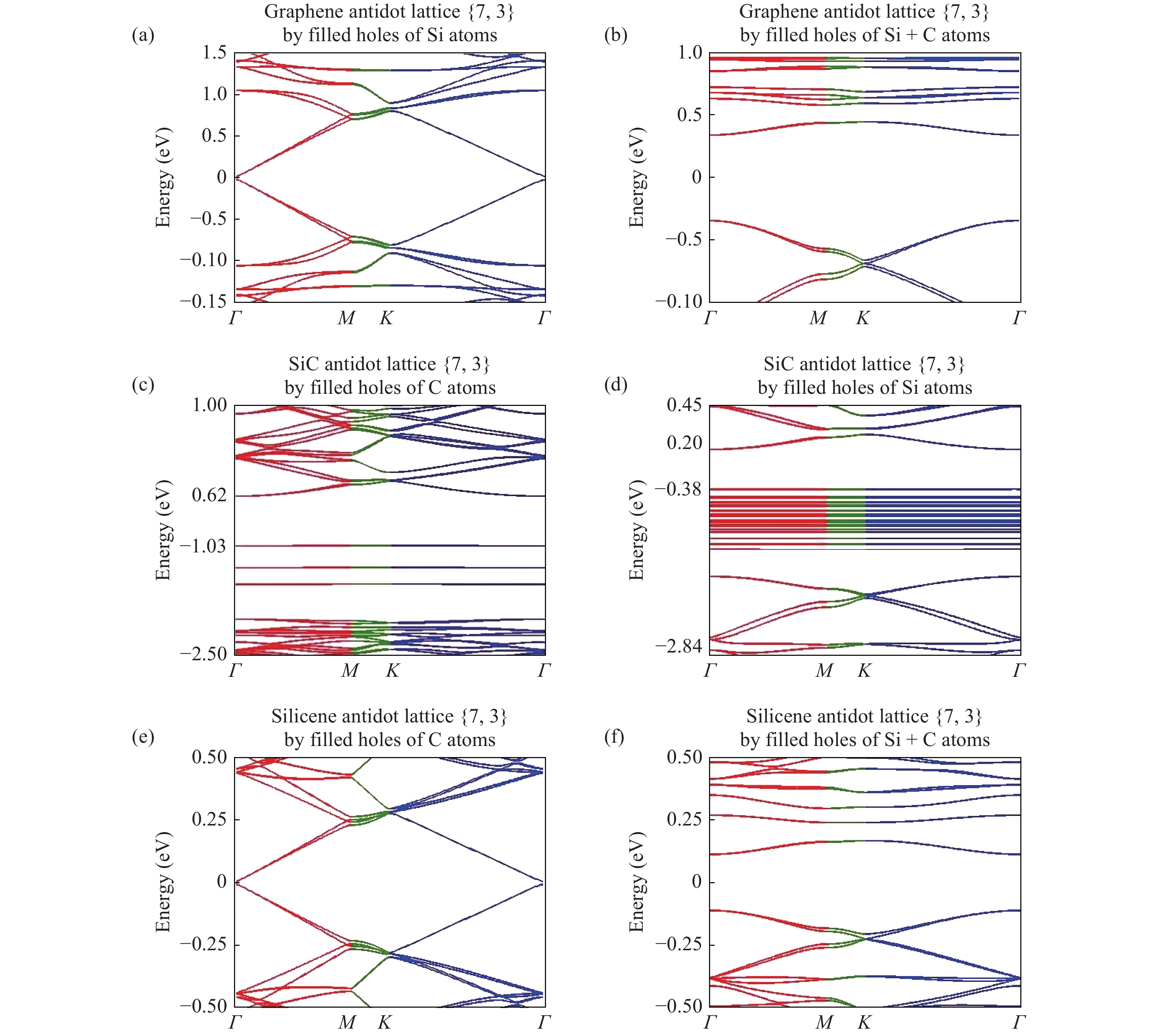
In this section using the tight-binding model taking into account the π orbitals, we obtain the band structure of the antidot lattices of graphene, silicene and SiC in which a triangular array of their corresponding holes are filled by other atoms. We study graphene antidot lattices filled by Si or Si + C atoms and silicene antidot lattices filled by C or Si + C atoms, and also SiC antidot lattices filled by Si or C atoms. For these antidot lattices we use the same notation of {L,R} in which L and R are the length of unit cells and the radius of the filled holes of the corresponding antidot lattices, respectively. Also we should emphasize that translation vectors of the corresponding antidot lattice are the same as the translation vectors presented in Fig. 2. By substituting Eqs. (2) and the on-site energies presented in Table 1 in the Hamiltonian of the corresponding antidot lattice by filled holes, we obtain the band structure of graphene, silicene and SiC antidot lattices including the triangular array of filled holes. Also it should be emphasized that here the number of corresponding levels for antidot with filled holes is N . The number of N used in the N×N Hamiltonian is the number of atoms in our hexagonal unit cell of the antidot lattice including the number of different atoms located in the hole region ( N=Nantidot-lattice+Nfilled-hole ). For example, for the case of {4, 1} configuration, we have 6 × 42 = 96 energy levels because we have N=96 atoms in our hexagonal unit cell of the antidot lattice. Also, for the case of {4,1} configuration we create a circular hole by replacing Nfilled-hole=6 atoms from the background by different type atoms. So for the case of {4,1} we have 90 of the background type atoms and also 6 different atoms in the hole region ( N=90+6 ). In Figs. 6(a)6(f) we have plotted the band structure of the graphene, silicene and SiC antidot lattices with indices {7,3} by filled holes taking into account the π -orbital states. We obtained that, antidot lattices with filled holes of C, Si and Si + C atoms are semiconductors with a direct band gap the same as their corresponding antidot lattices by empty holes.

Figure  2.  The illustration of triangular antidot lattice {4,1} in which a1 and a2 are translationvectors of the corresponding antidot lattice.

Also in Figs. 6(a) and 6(b), we obtained band gaps of 0.04 and 0.68 eV for the graphene antidot {7,3} filled by Si and Si + C atoms, respectively. Moreover in Figs. 6(c) and 6(d) we obtained the 1.65 and 0.58 eV band gaps for SiC antidot lattice {7,3} filled by C and Si atoms, respectively. Finally, in Figs. 6(e) and 6(f) we obtained the band gaps of silicene antidot lattice {7,3} filled by C and Si + C atoms. The band gaps of silicene antidot {7,3} filled by C and Si + C atoms are 0.01 eV and 0.22 eV, respectively. Also by comparing Fig. 3 with Fig. 6 we obtained that the band gaps of graphene, silicene and SiC antidot lattices by filled holes are less than the band gaps of the corresponding antidot lattices by empty holes with the same index {L,R}={7,3} .

As it is clear in Fig. 6, whereas the band gap of graphene (silicene) antidot with filled holes by Si (C) atoms is approximately the same as a complete graphene (silicene) sheet but graphene (silicene) antidot filled by Si + C atoms has a considerable band gap. Thus it is concluded that the graphene (silicene) antidot lattices including filled holes by Si (C) atoms are semimetal with almost zero band gap. Also by comparing Fig. 3(b) with Figs. 6(c) and 6(d) we obtained that, by filling of SiC antidot holes by Si or by C atoms the band gap decreases seriously. This decreasing of the band gap in SiC antidot lattice filled by C and Si atoms from 2.58 eV to energies less than 2 eV, which can be applied in electronics, occurs because of interactions between occupier atoms in the hole region with corresponding background atoms of antidot lattices. So, this decreasing of band gap is expectable. We know that, the difference of on-site energies of Si and C atoms in 2D structure of SiC sheet originates the band gap. So because on-site energies of filling atoms (C or Si) in the hole region of SiC antidot lattice are closer to on-site energies of background atoms (Si + C) as compared with the difference of on-site energies of atoms in the SiC antidot lattice by empty hole, the band gap decreases.

Figure  3.  (Color online) Band structures and their corresponding density of states of (a) silicene and (b) SiC antidot lattice that are obtained from the π -orbital model. These band structures are compared with (c) our reproduced band structures of graphene antidot lattice which is resulted by Pedersen et al. (Ref. [38]).
Figure  6.  (Color online) Band structures of graphene, silicene and SiC antidot lattices by filled holes of C or Si or Si + C atoms that were obtained from the π -orbital model.

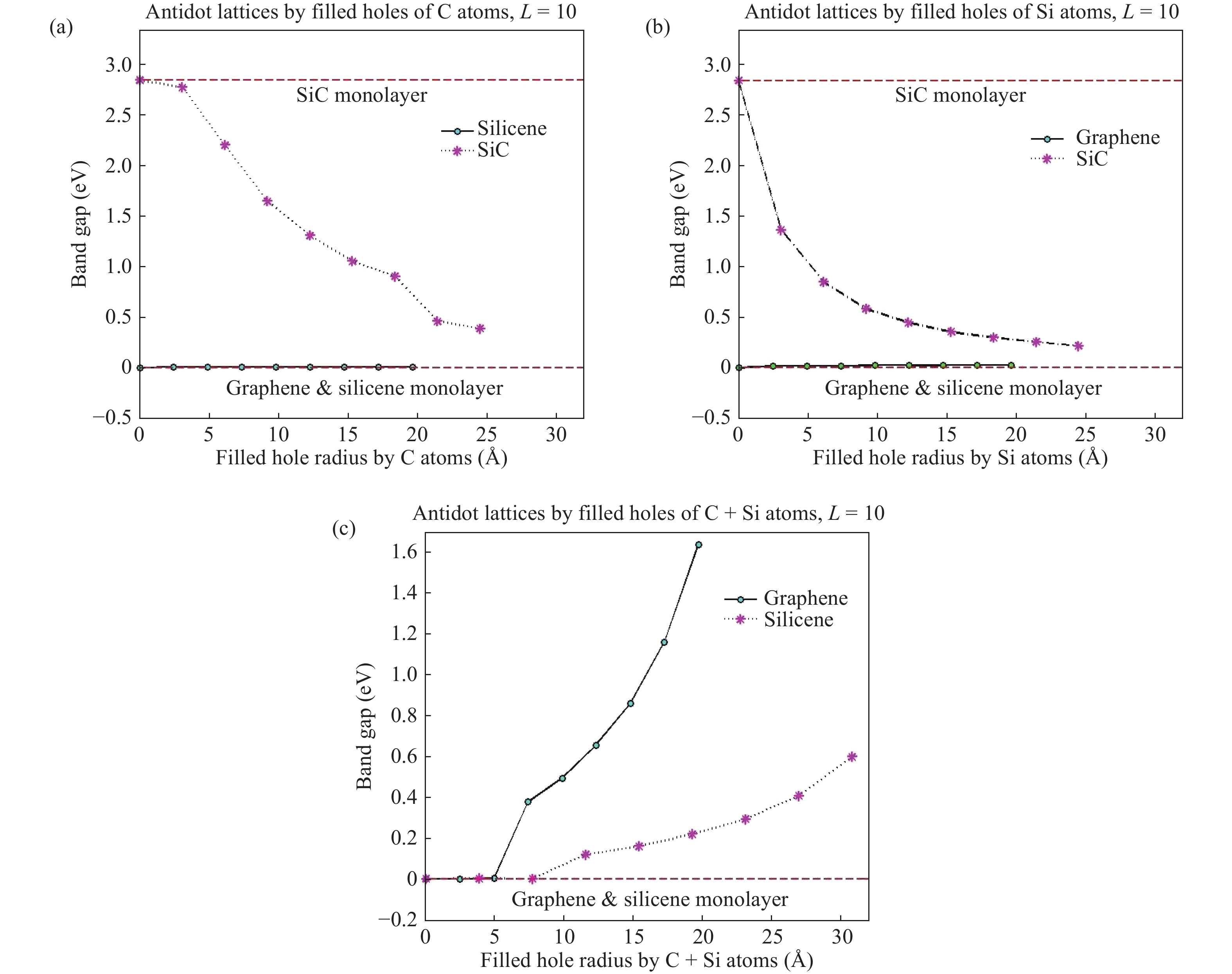
Also in Figs. 7(a)7(c), the dependence of band gaps on the holes diameter for graphene, silicene and SiC antidot lattices with filled holes are plotted. For SiC antidot lattice with holes filled by Si or C atoms, the band gap decreases by increasing of the hole diameter. As it is expected in the limit of R the band gap of SiC antidot lattice including the holes filled by Si or C atoms disappears and tends to the band gap of silicene or graphene sheet. This occurs because the number of C–C (Si–Si) bonds are more than the Si–C bonds and physics of the corresponding SiC antidot lattices approaches to the physics of graphene (silicene) 2D sheet. Also, we obtained a scaling rule for the band gap of the corresponding antidot lattices of SiC with holes filled by C or Si atoms as the following:

Eg(SiC - antidot){5.61(NholeNtotal)27.06(NholeNtotal)+2.63,filled by C,6.83(NholeNtotal)26.8(NholeNtotal)+1.67,filled by Si. (3)

These formulas are obtained by fitting and scaling numerically. In our obtained formulas for the effect of filled holes in SiC antidot (SiC monolayer including holes filled by C or by Si atoms), on the band gap energy we have a superposition of linear and parabolic terms. We think, the linear term is the result of the gapless part (graphene or silicene) in the hole region and the parabolic part comes from the SiC background part which is semiconducting with a finite gap. In addition in Figs. 7(a) and 7(b) we see that, by increasing the radius of holes of SiC antidot which are filled by C or by Si atoms the band gap decreases and finally tends to zero for sufficiently great holes. This is understandable, because by increasing the gapless part in the hole region the effect of the remainder of the gapped part of the antidot disappears and the gap suppresses. On the other hand in panel (c) of Fig. 7 we see that, for the case of graphene (silicene) antidot lattices with holes filled by Si + C atoms, by increasing the radius of filled hole the band gap increases. As it is expected in the limit of R the band gap of graphene (silicene) antidot including holes filled by Si + C atoms coincides with the band gap of the SiC sheet (2.85 eV). This occurs because the number of C–Si bonds are more than C–C (Si–Si) bonds and the physics of the corresponding graphene (silicene) antidot lattices tends to SiC sheet. Using the fitting of numerical results we obtain a formula for the energy gap of graphene antidot in terms of the radius of filled hole by Si + C atoms as following :

Figure  7.  (Color online) Band gap behavior of graphene, silicene and SiC antidot lattices by filled holes as a function of radius of filled holes by C, Si or Si + C atoms. The lower and upper red dash lines show the band gap of the 2D graphene (silicene) and the band gap of SiC monolayer, respectively.
Eg(graphene-antidot)0.09(NholeNtotal)2+2.15(NholeNtotal)+0.02. (4)

Also, in this gap equation we see a competition between the linear term for the gapless part with the parabolic part for the gapped one. In addition we should emphasize that the physics of our combined-system consisting of filled holes and background parts is more or less the result of the superposition of properties of two different parts. But this is not accurate because of the quantum mechanical interference effect in the system. So, the band gap of the combined system is not equal to the superposition of band gaps of two consisting parts of the system, exactly.

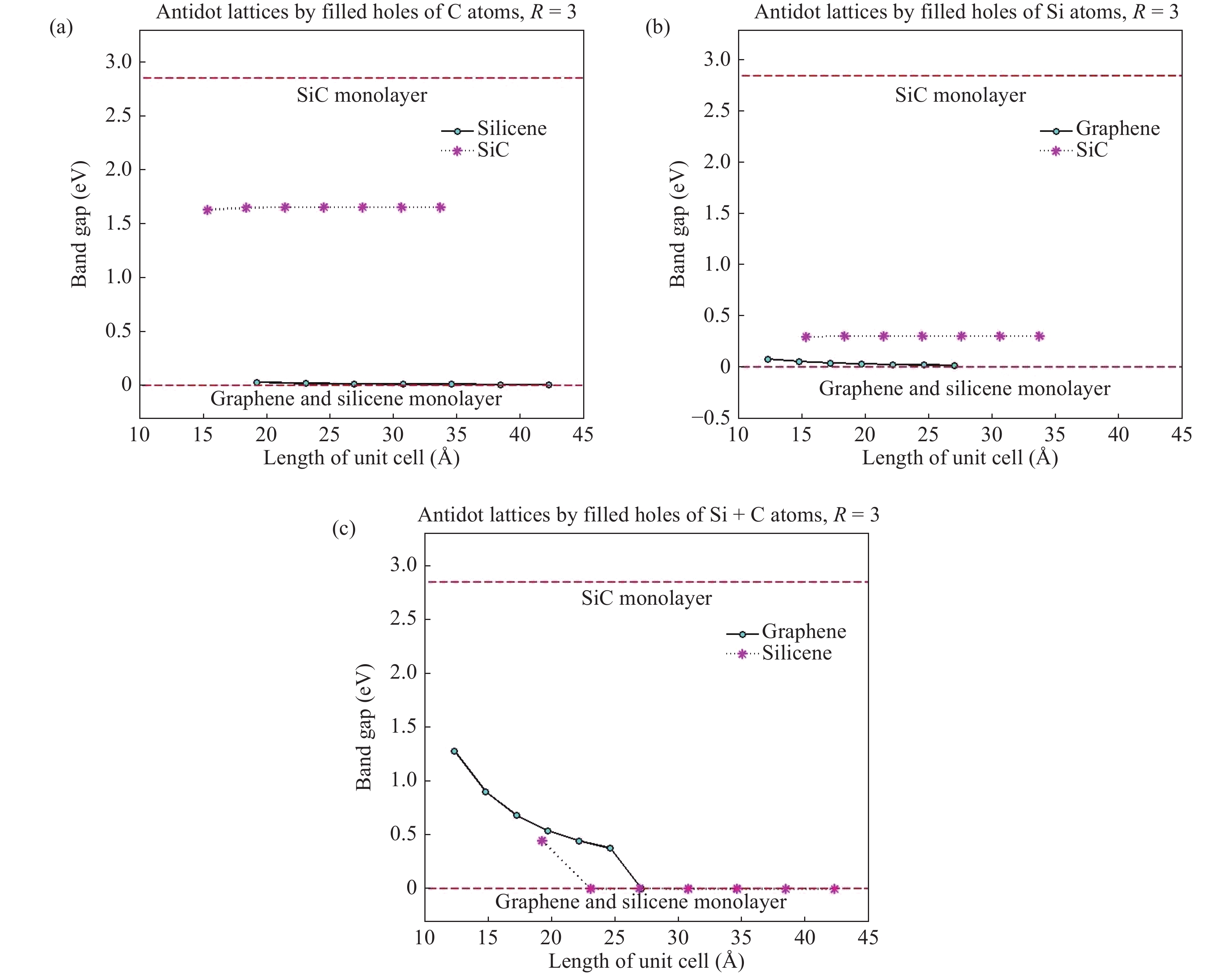
Finally, for the case of graphene (silicene) antidot lattices including holes filled by Si (C) atoms their band gap is constant over a wide range of the hole radius. Holes filled by Si (C) atoms do not have a serious influence on the physics of graphene (silicene) antidot because graphene and silicene sheets have similar physics and similar band gaps (both are gapless). So, graphene (silicene) antidot lattices filled by holes of Si (C) atoms remain semimetal with very small band gap. Also, in Figs. 8(a)8(c), the effect of the size of unit cell on the band gap for graphene, silicene and SiC antidot lattices by filled holes of C, Si or Si + C atoms is investigated. For the case of graphene (silicene) antidot lattices with holes filled by Si (C) atoms their band gap is constant over a wide range of unit cell size and they are almost semimetal. But if holes of the graphene or silicene antidot lattice are filled by Si + C atoms their corresponding band gap decreases by increasing of unit cell size ( La ). This latter case is expectable because the number of C–C (Si–Si) bonds is much more than the number of C–Si bonds, so the physics of the corresponding antidot is similar to the graphene (silicene) sheet and they will be semimetal. At the end, SiC antidot lattices with holes occupied by C (Si) atoms over a wide range of unit cell size are semiconductors with band gap between the band gap of graphene (silicene) sheet and the band gap of SiC sheet ( 0<Eg<2.85 ).

Figure  8.  (Color online) Band gap behavior of graphene, silicene and SiC antidot lattices with holes filled by other atoms (C, Si or Si + C) as a function of the length of their corresponding unit cell. The lower and upper red dash lines show the band gap of the 2D graphene (silicene) and the band gap of SiC monolayer, respectively.

The band structure of graphene, silicene and SiC antidot lattices with empty holes and also antidot lattices with filled holes by different atoms from the background atoms are studied using the nearest neighbor ( 1NN ) tight binding approach taking into account the π -orbital electrons, theoretically. We investigated the influence of the radius of holes, the length of unit cells of antidot lattices with empty and with filled holes on their band structures, numerically. Also, for antidot lattices with filled holes, the effect of the type of atoms which filled the holes (C, Si or Si + C atoms) on the band structures of antidot lattices is investigated. We obtained that, physical properties of silicene antidot lattice are similar to the graphene antidot lattices in Ref. [38] because both of graphene and silicene (C and Si) antidot lattices are made from the atoms of the same group of periodic table (IV) in the same structure (honeycomb). We obtained that the band gap of silicene antidot lattices with empty holes, increases by increasing the radius of holes and decreases by increasing the length of unit cells as for the case of graphene antidot in Ref. [38]. Also, we obtained that the band gap of silicene antidot lattices with empty holes is smaller than the band gap of graphene antidot lattices at the same size of radius and size of unit cell because the bond length of Si atoms in silicene is larger than the bond length of C atoms in graphene. In addition by numerical fitting of results, we obtained a linear relation between the band gap of the silicene antidot lattice and the radius of empty holes. We obtained that, the slope of linear relation for silicene is smaller than the case of graphene in Ref. [38] because of the difference between their Fermi velocities at the Dirac point. Also, we see that, the presence of holes at the silicene sheet replaces a gapless silicene to a gapped semiconductor which is suitable for application in transistors at room temperature. In addition, we obtained that the band gap of the SiC antidot lattice is almost constant over a wide range of the holes radius and the unit cells size. The band gap of SiC antidot lattices coincides with the band gap of SiC sheet without holes (2.85 eV). Also, we investigated the band structure of the corresponding antidot lattices with filled holes and observed that the type of atoms substituted in the hole regions (different atoms from background) may change the band gap. Changing of band gap by filling of hole is a result of superposition of wavefunctions of electrons of atoms in the hole region with the electrons of atoms in the background (complete sheet with holes). We see that the band gap of antidot with filled holes is not equal to the summation of band gaps of filled holes and background. This interesting result can be a result of quantum mechanical interference specially in the boundary region of holes with two different types of atoms. Also we obtained that, the band gap of silicene antidot lattice with holes filled by Si + C atoms (2.85 eV) is more than the zero band gap of silicene sheet. Also, we conclude that the type and the number of atoms in the hole region of antidot lattice controls the band gap. Moreover, the band structure of SiC antidot with holes filled by pure C or Si atoms is computed. We obtained that the band gap of SiC by filling of holes by C or Si atoms reduces to below 2 eV. This case is necessary for application of silicene-based parts in light-emitting devices or photoelectrochemistry. In addition we obtained that, filling of empty holes in graphene antidot lattice by Si or vice versa does not change the band gap from zero, seriously. This is understandable because both graphene and silicene sheets have zero gap. Finally, by scaling of our numerical results we obtain a band gap for SiC antidot with filled holes by C or by Si atoms as a function of hole radius. Our obtained function includes a parabolic function and a linear function of hole radius (fraction of replaced atoms). Parabolic terms is for the gapped part (SiC part) and the linear part is for the presence of the gapless part at the Dirac point (graphene or silicene part).


[1]
Bharech S, Kumar R. A review on the properties and applications of graphene. J Mater Sci Mechan Eng, 2015, 2(10): 70
[2]
Allen M J, Tung V C, Kaner R B. Honeycomb carbon: a review of graphene. Chem Rev, 2009, 110(1): 132
[3]
Choi W, Lee J W. Graphene: synthesis and applications. CRC Press, 2011
[4]
Chabot V, Higgins D, Yu A, et al. A review of graphene and graphene oxide sponge: material synthesis and applications to energy and the environment. Energy Environm Sci, 2014, 7(5): 1564 doi: 10.1039/c3ee43385d
[5]
Brunner K. Si/Ge nanostructures. Rep Prog Phys, 2001, 65(1): 27
[6]
Kara A, Enriquez H, Seitsonen A P, et al. A review on silicene—new candidate for electronics. Surf Sci Rep, 2012, 67(1): 1 doi: 10.1016/j.surfrep.2011.10.001
[7]
Chiew Y L, Cheong K Y. A review on the synthesis of SiC from plant-based biomasses. Mater Sci Eng B, 2011, 176(13): 951 doi: 10.1016/j.mseb.2011.05.037
[8]
Pecholt B, Gupta S, Molian P. Review of laser microscale processing of silicon carbide. J Laser Appl, 2011, 23(1): 012008 doi: 10.2351/1.3562522
[9]
Casady J, Johnson R. Status of silicon carbide (SiC) as a wide-band gap semiconductor for high-temperature applications: a review. Solid-State Electron, 1996, 39(10): 1409 doi: 10.1016/0038-1101(96)00045-7
[10]
Bekaroglu E, Topsakal M, Cahangirov S, et al. First-principles study of defects and adatoms in silicon carbide honeycomb structures. Phys Rev B, 2010, 81(7): 075433 doi: 10.1103/PhysRevB.81.075433
[11]
Ye X S, Shao Z G, Zhao H, et al. Electronic and optical properties of silicene nanomeshes. RSC Adv, 2014, 4(72): 37998 doi: 10.1039/C4RA03942D
[12]
Wright N G, Horsfall A B. SiC sensors: a review. J Phys D, 2007, 40(20): 6345 doi: 10.1088/0022-3727/40/20/S17
[13]
Shao Z G, Ye X S, Yang L, et al. First-principles calculation of intrinsic carrier mobility of silicene. J Appl Phys, 2013, 114(9): 093712 doi: 10.1063/1.4820526
[14]
Guzmán-Verri G G, Voon L L. Electronic structure of silicon-based nanostructures. Phys Rev B, 2007, 76(7): 075131 doi: 10.1103/PhysRevB.76.075131
[15]
Zheng F B, Zhang C W, Wang P J, et al. Novel half-metal and spin gapless semiconductor properties in N-doped silicene nanoribbons. J Appl Phys, 2013, 113(15): 154302 doi: 10.1063/1.4801882
[16]
Liu C C, Feng W, Yao Y. Quantum spin Hall effect in silicene and two-dimensional germanium. Phys Rev Lett, 2011, 107(7): 076802 doi: 10.1103/PhysRevLett.107.076802
[17]
Martinazzo R, Casolo S, Tantardini G F. Symmetry-induced band-gap opening in graphene superlattices. Phys Rev B, 2010, 81(24): 245420 doi: 10.1103/PhysRevB.81.245420
[18]
Trolle M L, Møller U S, Pedersen T G. Large and stable band gaps in spin-polarized graphene antidot lattices. Phys Rev B, 2013, 88(19): 195418 doi: 10.1103/PhysRevB.88.195418
[19]
Zhou W, Yan L, Wang Y, et al. SiC nanowires: a photocatalytic nanomaterial. Appl Phys Lett, 2006, 89(1): 013105 doi: 10.1063/1.2219139
[20]
Hu J Q, Bando Y, Zhan J H, et al. Fabrication of ZnS/SiC nanocables, SiC-shelled ZnS nanoribbons (and sheets), and SiC nanotubes (and tubes). Appl Phys Lett, 2004, 85(14): 2932 doi: 10.1063/1.1801168
[21]
De Padova P, Quaresima C, Ottaviani C, et al. Evidence of graphene-like electronic signature in silicene nanoribbons. Appl Phys Lett, 2010, 96(26): 261905 doi: 10.1063/1.3459143
[22]
Kim J, Kim Y H, Choi S H, et al. Curved silicon nanowires with ribbon-like cross sections by metal-assisted chemical etching. Acs Nano, 2011, 5(6): 5242 doi: 10.1021/nn2014358
[23]
Sun L, Li Y, Li Z, et al. Electronic structures of SiC nanoribbons. J Chem Phys, 2008, 129(17): 174114 doi: 10.1063/1.3006431
[24]
Baumeier B, Krüger P, Pollmann J. Structural, elastic, and electronic properties of SiC, BN, and BeO nanotubes. Phys Rev B, 2007, 76(8): 085407 doi: 10.1103/PhysRevB.76.085407
[25]
Menon M, Richter E, Mavrandonakis A, et al. Structure and stability of SiC nanotubes. Phys Rev B, 2004, 69(11): 115322 doi: 10.1103/PhysRevB.69.115322
[26]
Kara A, Vizzini S, Leandri C, et al. Silicon nano-ribbons on Ag (110): a computational investigation. J Phys: Condensed Matter, 2010, 22(4): 045004 doi: 10.1088/0953-8984/22/4/045004
[27]
Ding Y, Ni J. Electronic structures of silicon nanoribbons. Appl Phys Lett, 2009, 95(8): 083115 doi: 10.1063/1.3211968
[28]
Cahangirov S, Topsakal M, Aktürk E, et al. Two-and one-dimensional honeycomb structures of silicon and germanium. Phys Rev Lett, 2009, 102(23): 236804 doi: 10.1103/PhysRevLett.102.236804
[29]
Lehmann T, Ryndyk D A, Cuniberti G. Combined effect of strain and defects on the conductance of graphene nanoribbons. Phys Rev B, 2013, 88(12): 125420 doi: 10.1103/PhysRevB.88.125420
[30]
Sahin H, Ataca C, Ciraci S. Electronic and magnetic properties of graphane nanoribbons. Phys Rev B, 2010, 81(20): 205417 doi: 10.1103/PhysRevB.81.205417
[31]
Lu Y H, Feng Y P. Band-gap engineering with hybrid graphane–graphene nanoribbons. J Phys Chem C, 2009, 113(49): 20841 doi: 10.1021/jp9067284
[32]
Huang H, Wei D, Sun J, et al. Spatially resolved electronic structures of atomically precise armchair graphene nanoribbons. Sci Rep, 2012, 2: 983 doi: 10.1038/srep00983
[33]
Le Lay G, Aufray B, Léandri C, et al. Physics and chemistry of silicene nano-ribbons. Appl Surf Sci, 2009, 256(2): 524 doi: 10.1016/j.apsusc.2009.07.114
[34]
Balog R, Jørgensen B, Nilsson L, et al. Bandgap opening in graphene induced by patterned hydrogen adsorption. Nat Mater, 2010, 9(4): 315 doi: 10.1038/nmat2710
[35]
Zhang Y, Qin H, Cao E, et al. Ferromagnetism induced by intrinsic defects and boron substitution in single-wall SiC nanotubes. J Phys Chem A, 2011, 115(35): 9987 doi: 10.1021/jp109470r
[36]
Guzmán-Verri G G, Voon L L. Band structure of hydrogenated Si nanosheets and nanotubes. J Phys: Conden Matter, 2011, 23(14): 145502 doi: 10.1088/0953-8984/23/14/145502
[37]
Tachikawa H, Iyama T. Structures and electronic states of fluorinated graphene. Solid State Sci, 2014, 28: 41 doi: 10.1016/j.solidstatesciences.2013.12.014
[38]
Pedersen T G, Flindt C, Pedersen J, et al. Graphene antidot lattices: designed defects and spin qubits. Phys Rev Lett, 2008, 100(13): 136804 doi: 10.1103/PhysRevLett.100.136804
[39]
Ouyang F, Peng S, Yang Z, et al. Bandgap opening/closing of graphene antidot lattices with zigzag-edged hexagonal holes. Phys Chem Chem Phys, 2014, 16(38): 20524 doi: 10.1039/C4CP02090A
[40]
Oswald W, Wu Z. Energy gaps in graphene nanomeshes. Phys Rev B, 2012, 85(11): 115431 doi: 10.1103/PhysRevB.85.115431
[41]
Petersen R, Pedersen T G, Jauho A P. Clar sextets in square graphene antidot lattices. Physica E, 2012, 44(6): 967 doi: 10.1016/j.physe.2011.04.011
[42]
Zhang A, Teoh H F, Dai Z, et al. Band gap engineering in graphene and hexagonal BN antidot lattices: A first principles study. Appl Phys Lett, 2011, 98(2): 023105 doi: 10.1063/1.3536517
[43]
Petersen R, Pedersen T G, Jauho A P. Clar sextet analysis of triangular, rectangular, and honeycomb graphene antidot lattices. Acs Nano, 2010, 5(1): 523
[44]
Sahin H, Ciraci S. Structural, mechanical, and electronic properties of defect-patterned graphene nanomeshes from first principles. Phys Rev B, 2011, 84(3): 035452 doi: 10.1103/PhysRevB.84.035452
[45]
Ouyang F, Peng S, Liu Z, et al. Bandgap opening in graphene antidot lattices: the missing half. ACS Nano, 2011, 5(5): 4023 doi: 10.1021/nn200580w
[46]
Ouyang F, Yang Z, Xiao J, et al. Electronic structure and chemical modification of graphene antidot lattices. J Phys Chem C, 2010, 114(37): 15578 doi: 10.1021/jp1028454
[47]
Petersen R, Pedersen T G. Quasiparticle properties of graphene antidot lattices. Phys Rev B, 2009, 80(11): 113404 doi: 10.1103/PhysRevB.80.113404
[48]
Liu W, Wang Z F, Shi Q W, et al. Band-gap scaling of graphene nanohole superlattices. Phys Rev B, 2009, 80(23): 233405 doi: 10.1103/PhysRevB.80.233405
[49]
Fürst J A, Pedersen T G, Brandbyge M, et al. Density functional study of graphene antidot lattices: Roles of geometrical relaxation and spin. Phys Rev B, 2009, 80(11): 115117 doi: 10.1103/PhysRevB.80.115117
[50]
Yu D, Lupton E M, Liu M, et al. Collective magnetic behavior of graphene nanohole superlattices. Nano Res, 2008, 1(1): 56 doi: 10.1007/s12274-008-8007-6
[51]
Bai J, Zhong X, Jiang S, et al. Graphene nanomesh. Nat Nanotechnol, 2010, 5(3): 190 doi: 10.1038/nnano.2010.8
[52]
Kim M, Safron N S, Han E, at al. Fabrication and characterization of large-area, semiconducting nanoperforated graphene materials. Nano Lett, 2010, 10(4): 1125 doi: 10.1021/nl9032318
[53]
Liang X, Jung Y S, Wu S, et al. Formation of bandgap and subbands in graphene nanomeshes with sub-10 nm ribbon width fabricated via nanoimprint lithography. Nano Lett, 2010, 10(7): 2454 doi: 10.1021/nl100750v
[54]
Heydrich S, Hirmer M, Preis C, et al. Scanning Raman spectroscopy of graphene antidot lattices: evidence for systematic p-type doping. Appl Phys Lett, 2010, 97(4): 043113 doi: 10.1063/1.3474613
[55]
Shen T, Wu Y Q, Capano M A, et al. Magnetoconductance oscillations in graphene antidot arrays. Appl Phys Lett, 2008, 93(12): 122102 doi: 10.1063/1.2988725
[56]
Sinitskii A, Tour J M. Patterning graphene through the self-assembled templates: toward periodic two-dimensional graphene nanostructures with semiconductor properties. J Am Chem Soc, 2010, 132(42): 14730 doi: 10.1021/ja105426h
[57]
Freeman C L, Claeyssens F, Allan N L, et al. Graphitic nanofilms as precursors to wurtzite films: theory. Phys Rev Lett, 2006, 96(6): 066102 doi: 10.1103/PhysRevLett.96.066102
[58]
Chiappe D, Grazianetti C, Tallarida G, et al. Local electronic properties of corrugated silicene phases. Adv Mater, 2012, 25; 24(37): 5088
[59]
Sahin H, Cahangirov S, Topsakal M, et al. Monolayer honeycomb structures of group-IV elements and III–V binary compounds: first-principles calculations. Phys Rev B, 2009, 80(15): 155453 doi: 10.1103/PhysRevB.80.155453
[60]
Pan F, Wang Y, Jiang K, et al. Silicene nanomesh. Sci Rep, 2015, 5
[61]
Zhao K, Zhao M, Wang Z, et al. Tight-binding model for the electronic structures of SiC and BN nanoribbons. Physica E, 2010, 43(1): 440 doi: 10.1016/j.physe.2010.08.025
[62]
Saito R, Dresselhaus G, Dresselhaus M S. Physical properties of carbon nanotubes. World Scientific, 1998
[63]
Slater J C, Koster G F. Simplified LCAO method for the periodic potential problem. Phys Rev, 1954, 94(6): 1498 doi: 10.1103/PhysRev.94.1498
[64]
Jung J, MacDonald A H. Carrier density and magnetism in graphene zigzag nanoribbons. Phys Rev B, 2009, 79(23): 235433 doi: 10.1103/PhysRevB.79.235433
[65]
Hannewald K, Stojanović V M, Schellekens J M, et al. Theory of polaron bandwidth narrowing in organic molecular crystals. Phys Rev B, 2004, 69(7): 075211 doi: 10.1103/PhysRevB.69.075211
[66]
Novoselov K S, Geim A K, Morozov S, et al. Two-dimensional gas of massless Dirac fermions in graphene. Nature, 2005, 438(7065): 197 doi: 10.1038/nature04233
[67]
Berger C, Song Z, Li X, et al. Electronic confinement and coherence in patterned epitaxial graphene. Science, 2006, 312(5777): 1191 doi: 10.1126/science.1125925
[68]
Han M Y, Özyilmaz B, Zhang Y, et al. Energy band-gap engineering of graphene nanoribbons. Phys Rev Lett, 2007, 98(20): 206805 doi: 10.1103/PhysRevLett.98.206805
[69]
Geim A K, Novoselov K S. The rise of graphene. Nat Mater, 2007, 6(3): 183 doi: 10.1038/nmat1849
Fig. 1.  (Color online) (a) Hexagonal unit cell of a Si antidot lattice by side length 3 without any hole. Hexagonal unit cell of a Si antidot lattice with notation {3,1} by (b) empty hole and by (c) hole which is filled by silicon + carbon (Si + C) atoms instead of Si atoms. In both cases, the hole is arranged along the armchair direction. Also, the Si and C atoms are shown by blue and red points, respectively. Moreover, we show the border between regions of hole and background of unit cell with orange dash circle in which a is lattice constant.

Fig. 4.  (Color online) Band gap behavior of graphene, silicene and SiC antidot lattices by empty holes as a function of radius of empty hole. The lower and upper red dash lines show the band gap of the 2D graphene (silicene) and the band gap of SiC monolayer, respectively.

Fig. 5.  (Color online) Band gap behavior of graphene, silicene and SiC antidot lattices by empty holes as a function of the length of unit cell. The lower and upper red dash lines show the band gap of the 2D graphene (silicene) and the band gap of SiC monolayer, respectively.

Fig. 2.  The illustration of triangular antidot lattice {4,1} in which a1 and a2 are translationvectors of the corresponding antidot lattice.

Fig. 3.  (Color online) Band structures and their corresponding density of states of (a) silicene and (b) SiC antidot lattice that are obtained from the π -orbital model. These band structures are compared with (c) our reproduced band structures of graphene antidot lattice which is resulted by Pedersen et al. (Ref. [38]).

Fig. 6.  (Color online) Band structures of graphene, silicene and SiC antidot lattices by filled holes of C or Si or Si + C atoms that were obtained from the π -orbital model.

Fig. 7.  (Color online) Band gap behavior of graphene, silicene and SiC antidot lattices by filled holes as a function of radius of filled holes by C, Si or Si + C atoms. The lower and upper red dash lines show the band gap of the 2D graphene (silicene) and the band gap of SiC monolayer, respectively.

Fig. 8.  (Color online) Band gap behavior of graphene, silicene and SiC antidot lattices with holes filled by other atoms (C, Si or Si + C) as a function of the length of their corresponding unit cell. The lower and upper red dash lines show the band gap of the 2D graphene (silicene) and the band gap of SiC monolayer, respectively.

Table 1.   Two-center parameters of graphene, silicene and SiC antidot lattices related to π -orbitals of their corresponding sheets.

Parameter Graphene[61] Silicene[14] SiC[60]
(PPπ)IAB −3.033 −0.949 1.42
EAP 0 0 0
EBP 0 0 −2.85
DownLoad: CSV
[1]
Bharech S, Kumar R. A review on the properties and applications of graphene. J Mater Sci Mechan Eng, 2015, 2(10): 70
[2]
Allen M J, Tung V C, Kaner R B. Honeycomb carbon: a review of graphene. Chem Rev, 2009, 110(1): 132
[3]
Choi W, Lee J W. Graphene: synthesis and applications. CRC Press, 2011
[4]
Chabot V, Higgins D, Yu A, et al. A review of graphene and graphene oxide sponge: material synthesis and applications to energy and the environment. Energy Environm Sci, 2014, 7(5): 1564 doi: 10.1039/c3ee43385d
[5]
Brunner K. Si/Ge nanostructures. Rep Prog Phys, 2001, 65(1): 27
[6]
Kara A, Enriquez H, Seitsonen A P, et al. A review on silicene—new candidate for electronics. Surf Sci Rep, 2012, 67(1): 1 doi: 10.1016/j.surfrep.2011.10.001
[7]
Chiew Y L, Cheong K Y. A review on the synthesis of SiC from plant-based biomasses. Mater Sci Eng B, 2011, 176(13): 951 doi: 10.1016/j.mseb.2011.05.037
[8]
Pecholt B, Gupta S, Molian P. Review of laser microscale processing of silicon carbide. J Laser Appl, 2011, 23(1): 012008 doi: 10.2351/1.3562522
[9]
Casady J, Johnson R. Status of silicon carbide (SiC) as a wide-band gap semiconductor for high-temperature applications: a review. Solid-State Electron, 1996, 39(10): 1409 doi: 10.1016/0038-1101(96)00045-7
[10]
Bekaroglu E, Topsakal M, Cahangirov S, et al. First-principles study of defects and adatoms in silicon carbide honeycomb structures. Phys Rev B, 2010, 81(7): 075433 doi: 10.1103/PhysRevB.81.075433
[11]
Ye X S, Shao Z G, Zhao H, et al. Electronic and optical properties of silicene nanomeshes. RSC Adv, 2014, 4(72): 37998 doi: 10.1039/C4RA03942D
[12]
Wright N G, Horsfall A B. SiC sensors: a review. J Phys D, 2007, 40(20): 6345 doi: 10.1088/0022-3727/40/20/S17
[13]
Shao Z G, Ye X S, Yang L, et al. First-principles calculation of intrinsic carrier mobility of silicene. J Appl Phys, 2013, 114(9): 093712 doi: 10.1063/1.4820526
[14]
Guzmán-Verri G G, Voon L L. Electronic structure of silicon-based nanostructures. Phys Rev B, 2007, 76(7): 075131 doi: 10.1103/PhysRevB.76.075131
[15]
Zheng F B, Zhang C W, Wang P J, et al. Novel half-metal and spin gapless semiconductor properties in N-doped silicene nanoribbons. J Appl Phys, 2013, 113(15): 154302 doi: 10.1063/1.4801882
[16]
Liu C C, Feng W, Yao Y. Quantum spin Hall effect in silicene and two-dimensional germanium. Phys Rev Lett, 2011, 107(7): 076802 doi: 10.1103/PhysRevLett.107.076802
[17]
Martinazzo R, Casolo S, Tantardini G F. Symmetry-induced band-gap opening in graphene superlattices. Phys Rev B, 2010, 81(24): 245420 doi: 10.1103/PhysRevB.81.245420
[18]
Trolle M L, Møller U S, Pedersen T G. Large and stable band gaps in spin-polarized graphene antidot lattices. Phys Rev B, 2013, 88(19): 195418 doi: 10.1103/PhysRevB.88.195418
[19]
Zhou W, Yan L, Wang Y, et al. SiC nanowires: a photocatalytic nanomaterial. Appl Phys Lett, 2006, 89(1): 013105 doi: 10.1063/1.2219139
[20]
Hu J Q, Bando Y, Zhan J H, et al. Fabrication of ZnS/SiC nanocables, SiC-shelled ZnS nanoribbons (and sheets), and SiC nanotubes (and tubes). Appl Phys Lett, 2004, 85(14): 2932 doi: 10.1063/1.1801168
[21]
De Padova P, Quaresima C, Ottaviani C, et al. Evidence of graphene-like electronic signature in silicene nanoribbons. Appl Phys Lett, 2010, 96(26): 261905 doi: 10.1063/1.3459143
[22]
Kim J, Kim Y H, Choi S H, et al. Curved silicon nanowires with ribbon-like cross sections by metal-assisted chemical etching. Acs Nano, 2011, 5(6): 5242 doi: 10.1021/nn2014358
[23]
Sun L, Li Y, Li Z, et al. Electronic structures of SiC nanoribbons. J Chem Phys, 2008, 129(17): 174114 doi: 10.1063/1.3006431
[24]
Baumeier B, Krüger P, Pollmann J. Structural, elastic, and electronic properties of SiC, BN, and BeO nanotubes. Phys Rev B, 2007, 76(8): 085407 doi: 10.1103/PhysRevB.76.085407
[25]
Menon M, Richter E, Mavrandonakis A, et al. Structure and stability of SiC nanotubes. Phys Rev B, 2004, 69(11): 115322 doi: 10.1103/PhysRevB.69.115322
[26]
Kara A, Vizzini S, Leandri C, et al. Silicon nano-ribbons on Ag (110): a computational investigation. J Phys: Condensed Matter, 2010, 22(4): 045004 doi: 10.1088/0953-8984/22/4/045004
[27]
Ding Y, Ni J. Electronic structures of silicon nanoribbons. Appl Phys Lett, 2009, 95(8): 083115 doi: 10.1063/1.3211968
[28]
Cahangirov S, Topsakal M, Aktürk E, et al. Two-and one-dimensional honeycomb structures of silicon and germanium. Phys Rev Lett, 2009, 102(23): 236804 doi: 10.1103/PhysRevLett.102.236804
[29]
Lehmann T, Ryndyk D A, Cuniberti G. Combined effect of strain and defects on the conductance of graphene nanoribbons. Phys Rev B, 2013, 88(12): 125420 doi: 10.1103/PhysRevB.88.125420
[30]
Sahin H, Ataca C, Ciraci S. Electronic and magnetic properties of graphane nanoribbons. Phys Rev B, 2010, 81(20): 205417 doi: 10.1103/PhysRevB.81.205417
[31]
Lu Y H, Feng Y P. Band-gap engineering with hybrid graphane–graphene nanoribbons. J Phys Chem C, 2009, 113(49): 20841 doi: 10.1021/jp9067284
[32]
Huang H, Wei D, Sun J, et al. Spatially resolved electronic structures of atomically precise armchair graphene nanoribbons. Sci Rep, 2012, 2: 983 doi: 10.1038/srep00983
[33]
Le Lay G, Aufray B, Léandri C, et al. Physics and chemistry of silicene nano-ribbons. Appl Surf Sci, 2009, 256(2): 524 doi: 10.1016/j.apsusc.2009.07.114
[34]
Balog R, Jørgensen B, Nilsson L, et al. Bandgap opening in graphene induced by patterned hydrogen adsorption. Nat Mater, 2010, 9(4): 315 doi: 10.1038/nmat2710
[35]
Zhang Y, Qin H, Cao E, et al. Ferromagnetism induced by intrinsic defects and boron substitution in single-wall SiC nanotubes. J Phys Chem A, 2011, 115(35): 9987 doi: 10.1021/jp109470r
[36]
Guzmán-Verri G G, Voon L L. Band structure of hydrogenated Si nanosheets and nanotubes. J Phys: Conden Matter, 2011, 23(14): 145502 doi: 10.1088/0953-8984/23/14/145502
[37]
Tachikawa H, Iyama T. Structures and electronic states of fluorinated graphene. Solid State Sci, 2014, 28: 41 doi: 10.1016/j.solidstatesciences.2013.12.014
[38]
Pedersen T G, Flindt C, Pedersen J, et al. Graphene antidot lattices: designed defects and spin qubits. Phys Rev Lett, 2008, 100(13): 136804 doi: 10.1103/PhysRevLett.100.136804
[39]
Ouyang F, Peng S, Yang Z, et al. Bandgap opening/closing of graphene antidot lattices with zigzag-edged hexagonal holes. Phys Chem Chem Phys, 2014, 16(38): 20524 doi: 10.1039/C4CP02090A
[40]
Oswald W, Wu Z. Energy gaps in graphene nanomeshes. Phys Rev B, 2012, 85(11): 115431 doi: 10.1103/PhysRevB.85.115431
[41]
Petersen R, Pedersen T G, Jauho A P. Clar sextets in square graphene antidot lattices. Physica E, 2012, 44(6): 967 doi: 10.1016/j.physe.2011.04.011
[42]
Zhang A, Teoh H F, Dai Z, et al. Band gap engineering in graphene and hexagonal BN antidot lattices: A first principles study. Appl Phys Lett, 2011, 98(2): 023105 doi: 10.1063/1.3536517
[43]
Petersen R, Pedersen T G, Jauho A P. Clar sextet analysis of triangular, rectangular, and honeycomb graphene antidot lattices. Acs Nano, 2010, 5(1): 523
[44]
Sahin H, Ciraci S. Structural, mechanical, and electronic properties of defect-patterned graphene nanomeshes from first principles. Phys Rev B, 2011, 84(3): 035452 doi: 10.1103/PhysRevB.84.035452
[45]
Ouyang F, Peng S, Liu Z, et al. Bandgap opening in graphene antidot lattices: the missing half. ACS Nano, 2011, 5(5): 4023 doi: 10.1021/nn200580w
[46]
Ouyang F, Yang Z, Xiao J, et al. Electronic structure and chemical modification of graphene antidot lattices. J Phys Chem C, 2010, 114(37): 15578 doi: 10.1021/jp1028454
[47]
Petersen R, Pedersen T G. Quasiparticle properties of graphene antidot lattices. Phys Rev B, 2009, 80(11): 113404 doi: 10.1103/PhysRevB.80.113404
[48]
Liu W, Wang Z F, Shi Q W, et al. Band-gap scaling of graphene nanohole superlattices. Phys Rev B, 2009, 80(23): 233405 doi: 10.1103/PhysRevB.80.233405
[49]
Fürst J A, Pedersen T G, Brandbyge M, et al. Density functional study of graphene antidot lattices: Roles of geometrical relaxation and spin. Phys Rev B, 2009, 80(11): 115117 doi: 10.1103/PhysRevB.80.115117
[50]
Yu D, Lupton E M, Liu M, et al. Collective magnetic behavior of graphene nanohole superlattices. Nano Res, 2008, 1(1): 56 doi: 10.1007/s12274-008-8007-6
[51]
Bai J, Zhong X, Jiang S, et al. Graphene nanomesh. Nat Nanotechnol, 2010, 5(3): 190 doi: 10.1038/nnano.2010.8
[52]
Kim M, Safron N S, Han E, at al. Fabrication and characterization of large-area, semiconducting nanoperforated graphene materials. Nano Lett, 2010, 10(4): 1125 doi: 10.1021/nl9032318
[53]
Liang X, Jung Y S, Wu S, et al. Formation of bandgap and subbands in graphene nanomeshes with sub-10 nm ribbon width fabricated via nanoimprint lithography. Nano Lett, 2010, 10(7): 2454 doi: 10.1021/nl100750v
[54]
Heydrich S, Hirmer M, Preis C, et al. Scanning Raman spectroscopy of graphene antidot lattices: evidence for systematic p-type doping. Appl Phys Lett, 2010, 97(4): 043113 doi: 10.1063/1.3474613
[55]
Shen T, Wu Y Q, Capano M A, et al. Magnetoconductance oscillations in graphene antidot arrays. Appl Phys Lett, 2008, 93(12): 122102 doi: 10.1063/1.2988725
[56]
Sinitskii A, Tour J M. Patterning graphene through the self-assembled templates: toward periodic two-dimensional graphene nanostructures with semiconductor properties. J Am Chem Soc, 2010, 132(42): 14730 doi: 10.1021/ja105426h
[57]
Freeman C L, Claeyssens F, Allan N L, et al. Graphitic nanofilms as precursors to wurtzite films: theory. Phys Rev Lett, 2006, 96(6): 066102 doi: 10.1103/PhysRevLett.96.066102
[58]
Chiappe D, Grazianetti C, Tallarida G, et al. Local electronic properties of corrugated silicene phases. Adv Mater, 2012, 25; 24(37): 5088
[59]
Sahin H, Cahangirov S, Topsakal M, et al. Monolayer honeycomb structures of group-IV elements and III–V binary compounds: first-principles calculations. Phys Rev B, 2009, 80(15): 155453 doi: 10.1103/PhysRevB.80.155453
[60]
Pan F, Wang Y, Jiang K, et al. Silicene nanomesh. Sci Rep, 2015, 5
[61]
Zhao K, Zhao M, Wang Z, et al. Tight-binding model for the electronic structures of SiC and BN nanoribbons. Physica E, 2010, 43(1): 440 doi: 10.1016/j.physe.2010.08.025
[62]
Saito R, Dresselhaus G, Dresselhaus M S. Physical properties of carbon nanotubes. World Scientific, 1998
[63]
Slater J C, Koster G F. Simplified LCAO method for the periodic potential problem. Phys Rev, 1954, 94(6): 1498 doi: 10.1103/PhysRev.94.1498
[64]
Jung J, MacDonald A H. Carrier density and magnetism in graphene zigzag nanoribbons. Phys Rev B, 2009, 79(23): 235433 doi: 10.1103/PhysRevB.79.235433
[65]
Hannewald K, Stojanović V M, Schellekens J M, et al. Theory of polaron bandwidth narrowing in organic molecular crystals. Phys Rev B, 2004, 69(7): 075211 doi: 10.1103/PhysRevB.69.075211
[66]
Novoselov K S, Geim A K, Morozov S, et al. Two-dimensional gas of massless Dirac fermions in graphene. Nature, 2005, 438(7065): 197 doi: 10.1038/nature04233
[67]
Berger C, Song Z, Li X, et al. Electronic confinement and coherence in patterned epitaxial graphene. Science, 2006, 312(5777): 1191 doi: 10.1126/science.1125925
[68]
Han M Y, Özyilmaz B, Zhang Y, et al. Energy band-gap engineering of graphene nanoribbons. Phys Rev Lett, 2007, 98(20): 206805 doi: 10.1103/PhysRevLett.98.206805
[69]
Geim A K, Novoselov K S. The rise of graphene. Nat Mater, 2007, 6(3): 183 doi: 10.1038/nmat1849
1

Growth of oxidation-resistive silicene-like thin flakes and Si nanostructures on graphene

Naili Yue, Joshua Myers, Liqin Su, Wentao Wang, Fude Liu, et al.

Journal of Semiconductors, 2019, 40(6): 062001. doi: 10.1088/1674-4926/40/6/062001

2

Graphene-based flexible and wearable electronics

Tanmoy Das, Bhupendra K. Sharma, Ajit K. Katiyar, Jong-Hyun Ahn

Journal of Semiconductors, 2018, 39(1): 011007. doi: 10.1088/1674-4926/39/1/011007

3

Fabrication techniques and applications of flexible graphene-based electronic devices

Luqi Tao, Danyang Wang, Song Jiang, Ying Liu, Qianyi Xie, et al.

Journal of Semiconductors, 2016, 37(4): 041001. doi: 10.1088/1674-4926/37/4/041001

4

Comment on Chen et al. "Fabrication and photovoltaic conversion enhancement of graphene/n-Si Schottky barrier solar cells by electrophoretic deposition", Electrochimica Acta, 2014

Lara Valentic, Nima E. Gorji

Journal of Semiconductors, 2015, 36(9): 094012. doi: 10.1088/1674-4926/36/9/094012

5

Influence of the Trapping Effect on Temperature Characteristics in 4H-SiC MESFETs

Lü Hongliang, Zhang Yimen, Zhang Yuming, Che Yong, Wang Yuehu, et al.

Journal of Semiconductors, 2008, 29(2): 334-337.

6

Effect of Growth Gas Flow Rate on the Defects Density of SiC Single Crystal

Yang Ying, Lin Tao, Chen Zhiming

Journal of Semiconductors, 2008, 29(5): 851-854.

7

Recent Progress in SiC Monocrystal Growth and Wafer Machining

Jiang Shouzhen, Xu Xian'gang, Li Juan, Chen Xiufang, Wang Yingmin, et al.

Chinese Journal of Semiconductors , 2007, 28(5): 810-814.

8

Mo/Schottky Barrier Diodes on 4H-Silicon Carbide

Zhang Fasheng, Li Xinran

Chinese Journal of Semiconductors , 2007, 28(3): 435-438.

9

Gas Fluid Modeling of SiC Epitaxial Growth in Chemical Vapor Deposition Processes

Jia Renxu, Zhang Yimen, Zhang Yuming, Guo Hui

Chinese Journal of Semiconductors , 2007, 28(S1): 541-544.

10

Structural Analysis of the SiCGe Epitaxial Layer Grown on SiC Substrate

Li Lianbi, Chen Zhiming, Pu Hongbin, Lin Tao, Li Jia, et al.

Chinese Journal of Semiconductors , 2007, 28(S1): 123-126.

11

S-Band 1mm SiC MESFET with 2W Output on Semi-Insulated SiC Substrate

Cai Shujun, Pan Hongshu, Chen Hao, Li Liang, Zhao Zhenping, et al.

Chinese Journal of Semiconductors , 2006, 27(2): 266-269.

12

Direct Tunneling Effect in SiC Schottky Contacts

Tang Xiaoyan, Zhang Yimen, Zhang Yuming, Guo Hui, Zhang Lin, et al.

Chinese Journal of Semiconductors , 2006, 27(1): 174-177.

13

Ohmic Contact on SiC Using n+ Polysilicon/n+ SiC Heterojunction

Zhang Lin, Zhang Yimen, Zhang Yuming, Tang Xiaoyan

Chinese Journal of Semiconductors , 2006, 27(S1): 378-380.

14

C-V Characteristic Distortion in the Pinch-Off Mode of a Buried Channel MOS Structure in 4H-SiC

Gao Jinxia, Zhang Yimen, Zhang Yuming

Chinese Journal of Semiconductors , 2006, 27(7): 1259-1263.

15

Tight Binding of Photoluminescence in the SiC/nc-Si Multi-Layer Film

Liang Zhijun, Wang Zhibin, Wang Li, Zhao Fuli, Yang Shenghong, et al.

Chinese Journal of Semiconductors , 2006, 27(S1): 72-75.

16

Design and Simulation of a Light-Activated Darlington Transistor Based on a SiCGe/3C-SiC Hetero-Structure

Chen Zhiming, Ren Ping, Pu Hongbin

Chinese Journal of Semiconductors , 2006, 27(2): 254-257.

17

n-Type 4H-SiC Ohmic Contact

Chen Gang

Chinese Journal of Semiconductors , 2005, 26(S1): 273-276.

18

LPCVD Homoepitaxial Growth on Off-Axis Si-Face 4H-SiC(0001) Substrates

Wang Lei, Sun Guosheng, Gao Xin, Zhao Wanshun, Zhang Yongxing, et al.

Chinese Journal of Semiconductors , 2005, 26(S1): 113-116.

19

Turn-On Mechanism of a Light-Activated SiC Heterojuntion Darlington HBT

Pu Hongbin, Chen Zhiming

Chinese Journal of Semiconductors , 2005, 26(S1): 143-146.

20

High Quality Ultraviolet Photodetectors Based on Silicon Carbide

Huang Limin, Xie Jiachun, Liang Jin

Chinese Journal of Semiconductors , 2005, 26(S1): 256-260.

1. Zhou, W., Shui, S., Song, J. et al. Physical Properties of Doped Silicene Anodes for Na-Ion Battery: A First-Principles Study. Journal of Electronic Materials, 2025. doi:10.1007/s11664-025-11950-3
2. Liu, M., Li, S., Guo, Y. et al. 2D TMD-Based Lateral Heterostructures: Preparation, Property, and Application. Advanced Functional Materials, 2025. doi:10.1002/adfm.202500876
3. Kumar, G., Kumar, S., Kumar, A. et al. Predicting edge-localized monovacancy defects in zigzag graphene nanoribbons from Floquet quasienergy spectrum. Physical Review B, 2024, 109(23): 235401. doi:10.1103/PhysRevB.109.235401
4. Yilmaz, E., Yavuz, E. Use of transition metal dichalcogenides (TMDs) in analytical sample preparation applications. Talanta, 2024. doi:10.1016/j.talanta.2023.125086
5. Nouri, N., Nourbakhsh, Z., Rashedi, G. Stability of electronical properties of Antimony antidot nanostructure in the presence and in the absence of substrate. Physica B: Condensed Matter, 2023. doi:10.1016/j.physb.2023.414832
6. Durajski, A.P., Gruszka, K.M., Niegodajew, P. The influence of heteroatom doping on local properties of phosphorene monolayer. Scientific Reports, 2021, 11(1): 18494. doi:10.1038/s41598-021-98014-8
7. Zhao, B., Shen, D., Zhang, Z. et al. 2D Metallic Transition-Metal Dichalcogenides: Structures, Synthesis, Properties, and Applications. Advanced Functional Materials, 2021, 31(48): 2105132. doi:10.1002/adfm.202105132
8. Durajski, A.P., Gruszka, K.M., Niegodajew, P. First-principles study of a substitutionally doped phosphorene as anode material for Na-ion batteries. Applied Surface Science, 2020. doi:10.1016/j.apsusc.2020.147377
9. Roohi, H., Lotfi, T. Tuning the electronic properties of SiC nanosheets decorated by Lin (n = 1–3) for the anode of lithium-ion batteries. Molecular Physics, 2020, 118(23): e1786182. doi:10.1080/00268976.2020.1786182
10. Nouri, N., Rashedi, G., Karbaschi, H. Analysis of electronical properties of Bismuth and Silicene antidot in the presence of strain using the four-orbital tight-binding method. Physics Letters, Section A: General, Atomic and Solid State Physics, 2020, 384(17): 126364. doi:10.1016/j.physleta.2020.126364
11. Yan, G.-G., Liu, X.-F., Zhang, F. et al. Homoepitaxial growth on si-face (0001) on-axis 4H-SIC substrates. Materials Science Forum, 2019. doi:10.4028/www.scientific.net/MSF.954.31
12. Kalashnikov, A.V., Tuchin, A.V., Bityutskaja, L.A. Electronic structure of multilayer allotropes of 2D silicon carbide. Letters on Materials, 2019, 9(2): 173-178. doi:10.22226/2410-3535-2019-2-173-178
  • Search

    Advanced Search >>

    GET CITATION

    N. Nouri, G. Rashedi. Band structure of monolayer of graphene, silicene and silicon-carbide including a lattice of empty or filled holes[J]. Journal of Semiconductors, 2018, 39(8): 083001. doi: 10.1088/1674-4926/39/8/083001
    N. Nouri, G. Rashedi, Band structure of monolayer of graphene, silicene and silicon-carbide including a lattice of empty or filled holes[J]. J. Semicond., 2018, 39(8): 083001. doi: 10.1088/1674-4926/39/8/083001.
    shu

    Export: BibTex EndNote

    Article Metrics

    Article views: 5052 Times PDF downloads: 151 Times Cited by: 12 Times

    History

    Received: 22 August 2017 Revised: 18 February 2018 Online: Uncorrected proof: 17 April 2018Accepted Manuscript: 23 April 2018Published: 09 August 2018

    Catalog

      Email This Article

      User name:
      Email:*请输入正确邮箱
      Code:*验证码错误
      N. Nouri, G. Rashedi. Band structure of monolayer of graphene, silicene and silicon-carbide including a lattice of empty or filled holes[J]. Journal of Semiconductors, 2018, 39(8): 083001. doi: 10.1088/1674-4926/39/8/083001 ****N. Nouri, G. Rashedi, Band structure of monolayer of graphene, silicene and silicon-carbide including a lattice of empty or filled holes[J]. J. Semicond., 2018, 39(8): 083001. doi: 10.1088/1674-4926/39/8/083001.
      Citation:
      N. Nouri, G. Rashedi. Band structure of monolayer of graphene, silicene and silicon-carbide including a lattice of empty or filled holes[J]. Journal of Semiconductors, 2018, 39(8): 083001. doi: 10.1088/1674-4926/39/8/083001 ****
      N. Nouri, G. Rashedi, Band structure of monolayer of graphene, silicene and silicon-carbide including a lattice of empty or filled holes[J]. J. Semicond., 2018, 39(8): 083001. doi: 10.1088/1674-4926/39/8/083001.

      Band structure of monolayer of graphene, silicene and silicon-carbide including a lattice of empty or filled holes

      DOI: 10.1088/1674-4926/39/8/083001
      More Information
      • Corresponding author: E-mail: rashedi@phys.ui.ac.ir
      • Received Date: 2017-08-22
      • Revised Date: 2018-02-18
      • Published Date: 2018-08-01

      Catalog

        /

        DownLoad:  Full-Size Img  PowerPoint
        Return
        Return