


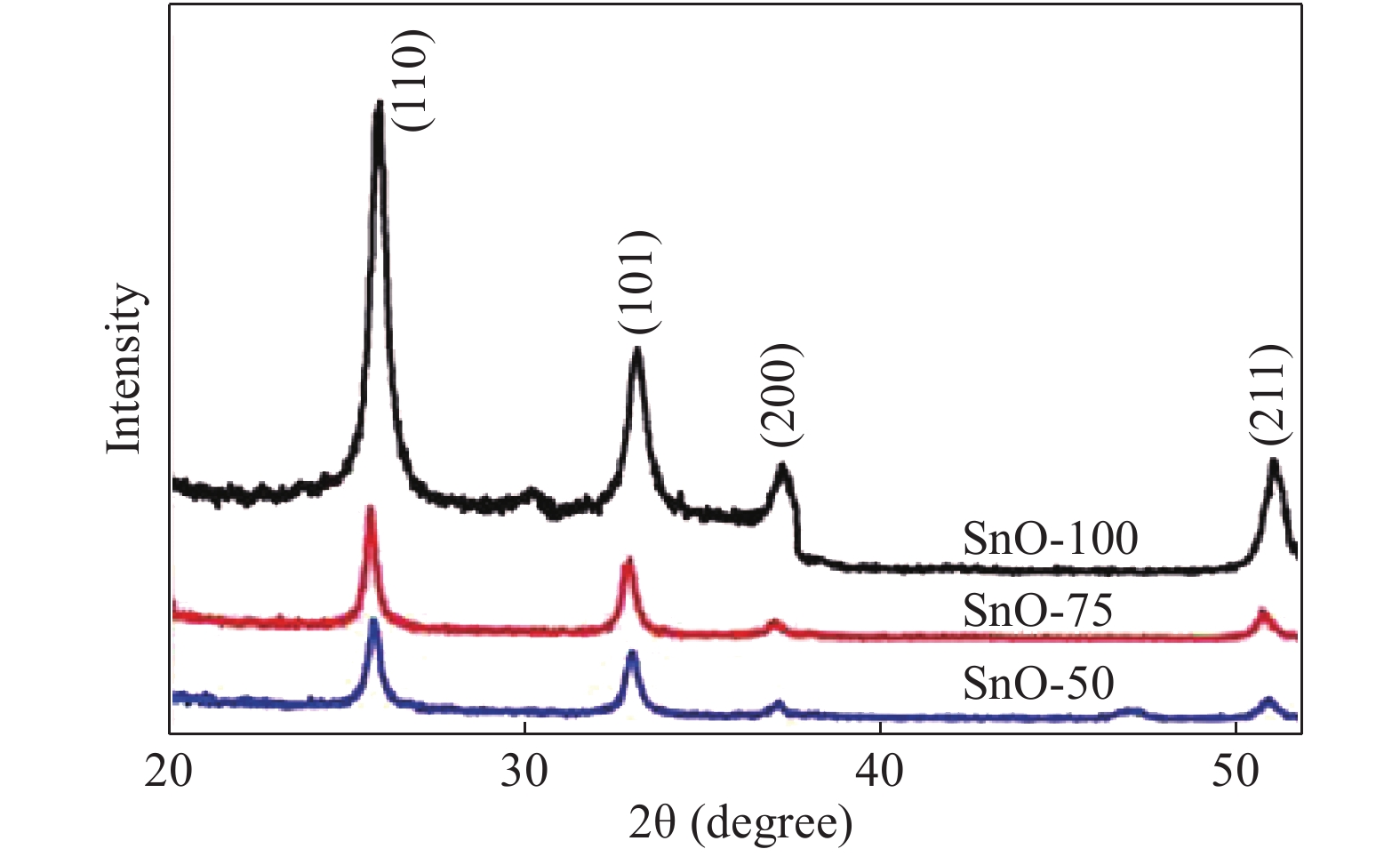
Fig. 1.
(Color online) XRD pattern of films deposited at 50 W (SnO-50), 75 W (SnO-75), and 100 W (SnO-100).
SEMICONDUCTOR MATERIALS
Nitin Kumar1, Bhawana Joshi1, and K. Asokan2
Corresponding author: Bhawana Joshi, bhawana@gbu.ac.in
Abstract: The role of deposition rate in the structural, optical and electrical properties of SnO2 thin films deposited by electron beam evaporation method is investigated by varying the deposition powers viz. 50, 75, and 100 W. The structural characterization of the films is done by X-ray diffraction (XRD) technique. The surface morphology of the films is studied by scanning electron microscopy (SEM). Rutherford back scattering (RBS) measurements revealed the thickness of the films ranging from 200 nm to 400 and also a change in the concentration of oxygen vacancies which is found to be the maximum in the film deposited at the lowest deposition rate. Optical absorption spectrum is recorded using the UV–V is spectroscopy and the films are found to be transparent in nature. A shift in the absorption edge is observed and is attributed to a different level of allowed energy states in conduction band minimum. The Hall effect and electrical measurements show a variation in the carrier concentrations, mobility and resistivity of the films. In order to explore a better compromise in electrical and optical properties for transparent electrode applications, skin depths calculations are also done to find the optimized values of carrier concentration and mobility.
Keywords: SnO2, oxygen vacancies, carrier concentration, deposition rate, electron beam evaporation
| [1] |
Elengovan E, Ramamurthy K. Optoelectronic properties of spray deposited SnO2:F thin films for window materials in solar cells. J Optoelect Adv Mater, 2003, 5: 45
|
| [2] |
Patil G, Kajale D D, Chavez D N, et al. Synthesis, characterization and gas sensing performance of SnO2 thin films prepared by spray pyrolysis. Bull Mater Sci, 2011, 34: 1 doi: 10.1007/s12034-011-0045-0
|
| [3] |
Presley R E, Munsee C L, Park C H, et al. Tin oxide transparent thin film transistors. J Phy D, 2004, 37: 2810 doi: 10.1088/0022-3727/37/20/006
|
| [4] |
Kolentsov K, Yourukova L, Zheliaskova A, et al. Some properties of doped SnO2 thin films used in EL and LC display structures. Bulg J Phy, 2004, 31: 87
|
| [5] |
Budak S, Miao G X, Ozdemir M, et al. Growth and characterization of single crystalline tin oxide (SnO2) nanowires. J Cryst Growth, 2006, 291: 405 doi: 10.1016/j.jcrysgro.2006.03.045
|
| [6] |
Kilic C, Zunger A. Origin of coexistence of conductivity and transparency in SnO2. Phys Rev Lett, 2002, 88: 9
|
| [7] |
Sumeyra M A Y, Emine T Y, Sakar F, et al. Synthesis, characterization and dielectric properties of SnO2 thin films. Spectochimica Acta A, 2014, 133: 60 doi: 10.1016/j.saa.2014.05.035
|
| [8] |
Slocombe D, Porch A, Pepper M, et al. The Mott transition and optimal performance of transparent conducting oxides in thin-film solar cells. Energy Environ Sci, 2012, 5: 5387 doi: 10.1039/C1EE02585F
|
| [9] |
Bansal S, Pandya D K, Kashyap S C. Electron transport and defect structure in highly conducting reactively sputtered ultrathin tin oxide films. Appl Phys Lett, 2014, 104: 082108 doi: 10.1063/1.4866869
|
| [10] |
Karamori M, Suzuki K, Ottya Y, et al. Analysis of change in the carrier concentration of SnO2 thin film gas sensor. Jpn J Appl Phys, 1994, 33: 6680 doi: 10.1143/JJAP.33.6680
|
| [11] |
Dang H P, Luc Q H, Le V H, et al. The influence of deposition temperature and annealing temperature on Ga-doped SnO2 films prepared by direct current magnetron sputtering. J Alloys Compnd, 2016, 687: 1012 doi: 10.1016/j.jallcom.2016.06.236
|
| [12] |
Cho Y, Parmar N S, Nahm S, et al. Full range optical and electrical properties of Zn-doped SnO2 and oxide/metal/oxide multilayer thin films deposited on flexible PET substrate. J Alloys Compnd, 2017, 694: 217 doi: 10.1016/j.jallcom.2016.09.293
|
| [13] |
Wang S, Huang J, Zhao Y, et al. Nanostructure SnO2 and supported Au catalysts: synthesis, characterization, and catalytic oxidation of CO. Mater Lett, 2006, 60: 1706 doi: 10.1016/j.matlet.2005.12.003
|
| [14] |
Khan A F, Mehmood M, Aslam M, et al. Characteristics of electron beam evaporated nanocrystalline SnO2 thin films annealed in air. Appl Surf Sci, 2010, 256: 2252 doi: 10.1016/j.apsusc.2009.10.047
|
| [15] |
Jiang J C, Lian K, Meletis E I. Influence of oxygen plasma treatment on the microstructure of SnOx thin films. Thin Solid Films, 2001, 411: 203
|
| [16] |
White M E, Tsai M Y, Wu F, et al. Plasma-assisted molecular beam epitaxy and characterization of SnO2 (101) on r-plane sapphire. J Vac Sci Technol A, 2008, 26: 1300 doi: 10.1116/1.2966423
|
| [17] |
Boyalı E, Baran V, Asar T, et al. Temperature dependent electron transport properties of degenerate SnO2 thin films. J Alloys Compnd, 2017, 692: 119 doi: 10.1016/j.jallcom.2016.09.011
|
| [18] |
Park Y C, Kim Y S, Seo H K, et al. ITO thin films deposited at different oxygen flow rates on Si(100) using the PEMOCVD method. Surf Coat Tech, 2002, 161: 62 doi: 10.1016/S0257-8972(02)00476-0
|
| [19] |
Kachouane A, Addou M, Bougrine A, et al. Preparation and characterization of tin-doped indium oxide films. Mater Chemy Phys, 2001, 70: 285 doi: 10.1016/S0254-0584(00)00492-2
|
| [20] |
Prathyusa T, Srikanth T, Reddy A S, et al. Effect of substrate bias voltage and substrate temperature on the physical properties of dc magnetron sputtered SnO2 thin films. Optik, 2011, 127: 9457
|
| [21] |
Minami T, Nanto H, Takata S. Highly conducting and transparent SnO2 thin films prepared by RF magnetron sputtering on low-temperature substrate. Jpn J Appl Phys, 1988, 27: L287 doi: 10.1143/JJAP.27.L287
|
| [22] |
Rus S F, Ward T Z, Herklotz A. Strain-induced optical band gap variation of SnO2 films. Thin Solid Film, 2016, 615: 103 doi: 10.1016/j.tsf.2016.06.057
|
| [23] |
He L, Cao Q, Feng X, et al. Structural, optical and electrical properties of epitaxial rutile SnO2 films grown on MgF2 (110) substrates by MOCVD. Ceram Int, 2018, 44: 869 doi: 10.1016/j.ceramint.2017.10.013
|
| [24] |
Mehraj S, Ansari M S, Alimuddin. Annealed SnO2 thin films: structural, electrical and their magnetic properties. Thin Solid Film, 2015, 589: 57 doi: 10.1016/j.tsf.2015.04.065
|
| [25] |
Deshpande S, Patil S, Kuchibhatla S V N T, et al. Size dependency variation in lattice parameter and valency states in nanocrystalline cerium oxide. Appl Phys Lett, 2005, 87: 133113 doi: 10.1063/1.2061873
|
| [26] |
Betty C A, Choudhury S. Charge carrier transport in nanocrystalline SnO2 thin film sensor and temperature dependence of toxic gas sensitivity. Sens Actuators B, 2016, 237: 787 doi: 10.1016/j.snb.2016.06.163
|
| [27] |
Ansari S G, Boroojordian P, Sainkar S R, et al. Grain size effects on H2 gas sensitivity of thick film resistor using SnO2 nanoparticles. Thin Solid Film, 1997, 295: 271 doi: 10.1016/S0040-6090(96)09152-3
|
| [28] |
Deal B E, Grove A S. General relationship for the thermal oxidation of silicon. J Appl Phys, 1965, 36: 3770 doi: 10.1063/1.1713945
|
| [29] |
Malevu T D, Ocaya R O. Effect of annealing temperature on structural, morphology and optical properties of ZnO nano-needles prepared by zinc-air cell system method. Int J Electrochem Sci, 2015, 10: 1752
|
| [30] |
Meng Q, Wang J, Huang J, et al. Impact of oxygen vacancy on band structure engineering of n–p Co doped anatase TiO2. Chin J Chem Phys, 2015, 28: 155 doi: 10.1063/1674-0068/28/cjcp1411196
|
| [31] |
Gall D. Electronic mean free path in elemental metals. J Appl Phys, 2016, 119: 085101 doi: 10.1063/1.4942216
|
| [32] |
Jarzebski Z M, Morton J P. Physical properties of SnO2 materials II. electrical properties. J Electrochem Soc, 1976, 123: 299C doi: 10.1149/1.2133090
|
| [33] |
Dominguez J E, Fu L, Pan X Q. Effect of crystal defects on the electrical properties in epitaxial tin dioxide thin films. Appl Phys Lett, 2002, 81: 5168 doi: 10.1063/1.1530745
|
| [34] |
Jarzebski Z M, Morton J P. Physical properties of SnO2 materials III. optical properties. J Electrochem Soc, 1976, 123: 333C doi: 10.1149/1.2132647
|
| [35] |
Masahiro N, Shigeo S, Shoji M. Electron effective mass of SnO2. J Phys Soc Jpn, 1965, 20: 1093 doi: 10.1143/JPSJ.20.1093
|
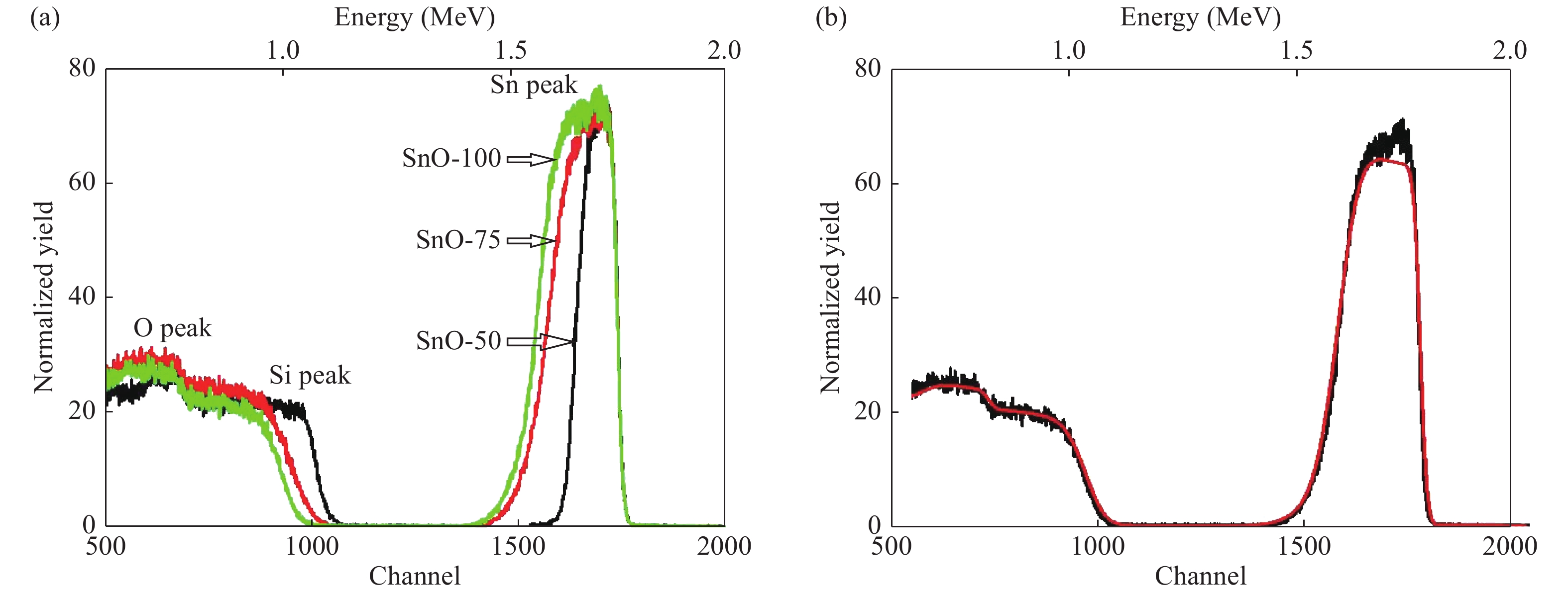
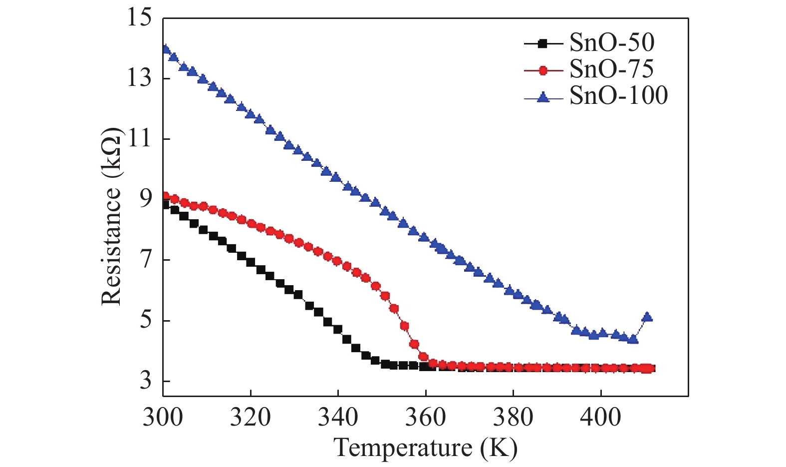
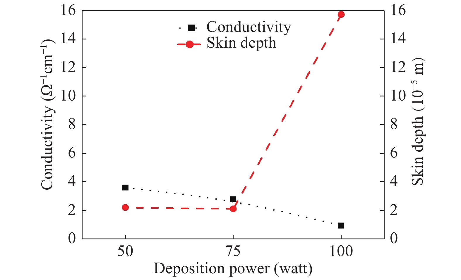
Table 1. The change in lattice constants is attributed to the lattice strain produced by the variation in deposition power. This also results in change in particle size and formation of oxygen vacancies[25] in the matrix of the films.
| Sample | a = b (Ǻ) | c (Ǻ) | Crystallite size (nm) |
| SnO-50 | 4.744 | 3.187 | 21 |
| SnO-75 | 4.741 | 3.188 | 19 |
| SnO-100 | 4.747 | 3.190 | 15 |
 DownLoad: CSV
Table 2. Simulated results of RBS spectra for SnO-50, SnO-75, and SnO-100 films.
| Sample | SnO-50 | SnO-75 | SnO-100 |
| Thickness (nm) | 200 | 250 | 400 |
| Concentration (Sn) | 1 | 1 | 1 |
| Concentration (O) | 1.7 | 1.9 | 2.0 |
DownLoad: CSV
Table 3. The results of Hall Effect, resistance measurements and calculated values of Fermi energy, Fermi velocities and electron mean free path for SnO-50, SnO-75, and SnO-100.
| Physical quantity | SnO-50 | SnO-75 | SnO-100 |
| Carrier concentration (1018 cm−3) | 4.615 | 4.346 | 1.018 |
| Mobility (cm2/(V·s)) | 4.848 | 3.972 | 5.700 |
| Resistivity (Ω·cm) | 0.279 | 0.3616 | 1.076 |
| Fermi energy (eV) | 0.0162 | 0.0155 | 0.006 |
| Fermi velocity (104 m/s) | 6 | 5 | 0.04 |
| Mean free path (nm) | 16.2 | 12.76 | 0.12 |
DownLoad: CSV
| [1] |
Elengovan E, Ramamurthy K. Optoelectronic properties of spray deposited SnO2:F thin films for window materials in solar cells. J Optoelect Adv Mater, 2003, 5: 45
|
| [2] |
Patil G, Kajale D D, Chavez D N, et al. Synthesis, characterization and gas sensing performance of SnO2 thin films prepared by spray pyrolysis. Bull Mater Sci, 2011, 34: 1 doi: 10.1007/s12034-011-0045-0
|
| [3] |
Presley R E, Munsee C L, Park C H, et al. Tin oxide transparent thin film transistors. J Phy D, 2004, 37: 2810 doi: 10.1088/0022-3727/37/20/006
|
| [4] |
Kolentsov K, Yourukova L, Zheliaskova A, et al. Some properties of doped SnO2 thin films used in EL and LC display structures. Bulg J Phy, 2004, 31: 87
|
| [5] |
Budak S, Miao G X, Ozdemir M, et al. Growth and characterization of single crystalline tin oxide (SnO2) nanowires. J Cryst Growth, 2006, 291: 405 doi: 10.1016/j.jcrysgro.2006.03.045
|
| [6] |
Kilic C, Zunger A. Origin of coexistence of conductivity and transparency in SnO2. Phys Rev Lett, 2002, 88: 9
|
| [7] |
Sumeyra M A Y, Emine T Y, Sakar F, et al. Synthesis, characterization and dielectric properties of SnO2 thin films. Spectochimica Acta A, 2014, 133: 60 doi: 10.1016/j.saa.2014.05.035
|
| [8] |
Slocombe D, Porch A, Pepper M, et al. The Mott transition and optimal performance of transparent conducting oxides in thin-film solar cells. Energy Environ Sci, 2012, 5: 5387 doi: 10.1039/C1EE02585F
|
| [9] |
Bansal S, Pandya D K, Kashyap S C. Electron transport and defect structure in highly conducting reactively sputtered ultrathin tin oxide films. Appl Phys Lett, 2014, 104: 082108 doi: 10.1063/1.4866869
|
| [10] |
Karamori M, Suzuki K, Ottya Y, et al. Analysis of change in the carrier concentration of SnO2 thin film gas sensor. Jpn J Appl Phys, 1994, 33: 6680 doi: 10.1143/JJAP.33.6680
|
| [11] |
Dang H P, Luc Q H, Le V H, et al. The influence of deposition temperature and annealing temperature on Ga-doped SnO2 films prepared by direct current magnetron sputtering. J Alloys Compnd, 2016, 687: 1012 doi: 10.1016/j.jallcom.2016.06.236
|
| [12] |
Cho Y, Parmar N S, Nahm S, et al. Full range optical and electrical properties of Zn-doped SnO2 and oxide/metal/oxide multilayer thin films deposited on flexible PET substrate. J Alloys Compnd, 2017, 694: 217 doi: 10.1016/j.jallcom.2016.09.293
|
| [13] |
Wang S, Huang J, Zhao Y, et al. Nanostructure SnO2 and supported Au catalysts: synthesis, characterization, and catalytic oxidation of CO. Mater Lett, 2006, 60: 1706 doi: 10.1016/j.matlet.2005.12.003
|
| [14] |
Khan A F, Mehmood M, Aslam M, et al. Characteristics of electron beam evaporated nanocrystalline SnO2 thin films annealed in air. Appl Surf Sci, 2010, 256: 2252 doi: 10.1016/j.apsusc.2009.10.047
|
| [15] |
Jiang J C, Lian K, Meletis E I. Influence of oxygen plasma treatment on the microstructure of SnOx thin films. Thin Solid Films, 2001, 411: 203
|
| [16] |
White M E, Tsai M Y, Wu F, et al. Plasma-assisted molecular beam epitaxy and characterization of SnO2 (101) on r-plane sapphire. J Vac Sci Technol A, 2008, 26: 1300 doi: 10.1116/1.2966423
|
| [17] |
Boyalı E, Baran V, Asar T, et al. Temperature dependent electron transport properties of degenerate SnO2 thin films. J Alloys Compnd, 2017, 692: 119 doi: 10.1016/j.jallcom.2016.09.011
|
| [18] |
Park Y C, Kim Y S, Seo H K, et al. ITO thin films deposited at different oxygen flow rates on Si(100) using the PEMOCVD method. Surf Coat Tech, 2002, 161: 62 doi: 10.1016/S0257-8972(02)00476-0
|
| [19] |
Kachouane A, Addou M, Bougrine A, et al. Preparation and characterization of tin-doped indium oxide films. Mater Chemy Phys, 2001, 70: 285 doi: 10.1016/S0254-0584(00)00492-2
|
| [20] |
Prathyusa T, Srikanth T, Reddy A S, et al. Effect of substrate bias voltage and substrate temperature on the physical properties of dc magnetron sputtered SnO2 thin films. Optik, 2011, 127: 9457
|
| [21] |
Minami T, Nanto H, Takata S. Highly conducting and transparent SnO2 thin films prepared by RF magnetron sputtering on low-temperature substrate. Jpn J Appl Phys, 1988, 27: L287 doi: 10.1143/JJAP.27.L287
|
| [22] |
Rus S F, Ward T Z, Herklotz A. Strain-induced optical band gap variation of SnO2 films. Thin Solid Film, 2016, 615: 103 doi: 10.1016/j.tsf.2016.06.057
|
| [23] |
He L, Cao Q, Feng X, et al. Structural, optical and electrical properties of epitaxial rutile SnO2 films grown on MgF2 (110) substrates by MOCVD. Ceram Int, 2018, 44: 869 doi: 10.1016/j.ceramint.2017.10.013
|
| [24] |
Mehraj S, Ansari M S, Alimuddin. Annealed SnO2 thin films: structural, electrical and their magnetic properties. Thin Solid Film, 2015, 589: 57 doi: 10.1016/j.tsf.2015.04.065
|
| [25] |
Deshpande S, Patil S, Kuchibhatla S V N T, et al. Size dependency variation in lattice parameter and valency states in nanocrystalline cerium oxide. Appl Phys Lett, 2005, 87: 133113 doi: 10.1063/1.2061873
|
| [26] |
Betty C A, Choudhury S. Charge carrier transport in nanocrystalline SnO2 thin film sensor and temperature dependence of toxic gas sensitivity. Sens Actuators B, 2016, 237: 787 doi: 10.1016/j.snb.2016.06.163
|
| [27] |
Ansari S G, Boroojordian P, Sainkar S R, et al. Grain size effects on H2 gas sensitivity of thick film resistor using SnO2 nanoparticles. Thin Solid Film, 1997, 295: 271 doi: 10.1016/S0040-6090(96)09152-3
|
| [28] |
Deal B E, Grove A S. General relationship for the thermal oxidation of silicon. J Appl Phys, 1965, 36: 3770 doi: 10.1063/1.1713945
|
| [29] |
Malevu T D, Ocaya R O. Effect of annealing temperature on structural, morphology and optical properties of ZnO nano-needles prepared by zinc-air cell system method. Int J Electrochem Sci, 2015, 10: 1752
|
| [30] |
Meng Q, Wang J, Huang J, et al. Impact of oxygen vacancy on band structure engineering of n–p Co doped anatase TiO2. Chin J Chem Phys, 2015, 28: 155 doi: 10.1063/1674-0068/28/cjcp1411196
|
| [31] |
Gall D. Electronic mean free path in elemental metals. J Appl Phys, 2016, 119: 085101 doi: 10.1063/1.4942216
|
| [32] |
Jarzebski Z M, Morton J P. Physical properties of SnO2 materials II. electrical properties. J Electrochem Soc, 1976, 123: 299C doi: 10.1149/1.2133090
|
| [33] |
Dominguez J E, Fu L, Pan X Q. Effect of crystal defects on the electrical properties in epitaxial tin dioxide thin films. Appl Phys Lett, 2002, 81: 5168 doi: 10.1063/1.1530745
|
| [34] |
Jarzebski Z M, Morton J P. Physical properties of SnO2 materials III. optical properties. J Electrochem Soc, 1976, 123: 333C doi: 10.1149/1.2132647
|
| [35] |
Masahiro N, Shigeo S, Shoji M. Electron effective mass of SnO2. J Phys Soc Jpn, 1965, 20: 1093 doi: 10.1143/JPSJ.20.1093
|


Article views: 5184 Times PDF downloads: 107 Times Cited by: 0 Times
Received: 31 August 2017 Revised: 09 February 2018 Online: Accepted Manuscript: 12 April 2018Uncorrected proof: 20 April 2018Published: 09 August 2018
| Citation: |
Nitin Kumar, Bhawana Joshi, K. Asokan. Influence of deposition rate on the structural, optical and electrical properties of electron beam evaporated SnO2 thin films for transparent conducting electrode applications[J]. Journal of Semiconductors, 2018, 39(8): 083002. doi: 10.1088/1674-4926/39/8/083002
****
N Kumar, B Joshi, K Asokan, Influence of deposition rate on the structural, optical and electrical properties of electron beam evaporated SnO2 thin films for transparent conducting electrode applications[J]. J. Semicond., 2018, 39(8): 083002. doi: 10.1088/1674-4926/39/8/083002.

|
| [1] |
Elengovan E, Ramamurthy K. Optoelectronic properties of spray deposited SnO2:F thin films for window materials in solar cells. J Optoelect Adv Mater, 2003, 5: 45
|
| [2] |
Patil G, Kajale D D, Chavez D N, et al. Synthesis, characterization and gas sensing performance of SnO2 thin films prepared by spray pyrolysis. Bull Mater Sci, 2011, 34: 1 doi: 10.1007/s12034-011-0045-0
|
| [3] |
Presley R E, Munsee C L, Park C H, et al. Tin oxide transparent thin film transistors. J Phy D, 2004, 37: 2810 doi: 10.1088/0022-3727/37/20/006
|
| [4] |
Kolentsov K, Yourukova L, Zheliaskova A, et al. Some properties of doped SnO2 thin films used in EL and LC display structures. Bulg J Phy, 2004, 31: 87
|
| [5] |
Budak S, Miao G X, Ozdemir M, et al. Growth and characterization of single crystalline tin oxide (SnO2) nanowires. J Cryst Growth, 2006, 291: 405 doi: 10.1016/j.jcrysgro.2006.03.045
|
| [6] |
Kilic C, Zunger A. Origin of coexistence of conductivity and transparency in SnO2. Phys Rev Lett, 2002, 88: 9
|
| [7] |
Sumeyra M A Y, Emine T Y, Sakar F, et al. Synthesis, characterization and dielectric properties of SnO2 thin films. Spectochimica Acta A, 2014, 133: 60 doi: 10.1016/j.saa.2014.05.035
|
| [8] |
Slocombe D, Porch A, Pepper M, et al. The Mott transition and optimal performance of transparent conducting oxides in thin-film solar cells. Energy Environ Sci, 2012, 5: 5387 doi: 10.1039/C1EE02585F
|
| [9] |
Bansal S, Pandya D K, Kashyap S C. Electron transport and defect structure in highly conducting reactively sputtered ultrathin tin oxide films. Appl Phys Lett, 2014, 104: 082108 doi: 10.1063/1.4866869
|
| [10] |
Karamori M, Suzuki K, Ottya Y, et al. Analysis of change in the carrier concentration of SnO2 thin film gas sensor. Jpn J Appl Phys, 1994, 33: 6680 doi: 10.1143/JJAP.33.6680
|
| [11] |
Dang H P, Luc Q H, Le V H, et al. The influence of deposition temperature and annealing temperature on Ga-doped SnO2 films prepared by direct current magnetron sputtering. J Alloys Compnd, 2016, 687: 1012 doi: 10.1016/j.jallcom.2016.06.236
|
| [12] |
Cho Y, Parmar N S, Nahm S, et al. Full range optical and electrical properties of Zn-doped SnO2 and oxide/metal/oxide multilayer thin films deposited on flexible PET substrate. J Alloys Compnd, 2017, 694: 217 doi: 10.1016/j.jallcom.2016.09.293
|
| [13] |
Wang S, Huang J, Zhao Y, et al. Nanostructure SnO2 and supported Au catalysts: synthesis, characterization, and catalytic oxidation of CO. Mater Lett, 2006, 60: 1706 doi: 10.1016/j.matlet.2005.12.003
|
| [14] |
Khan A F, Mehmood M, Aslam M, et al. Characteristics of electron beam evaporated nanocrystalline SnO2 thin films annealed in air. Appl Surf Sci, 2010, 256: 2252 doi: 10.1016/j.apsusc.2009.10.047
|
| [15] |
Jiang J C, Lian K, Meletis E I. Influence of oxygen plasma treatment on the microstructure of SnOx thin films. Thin Solid Films, 2001, 411: 203
|
| [16] |
White M E, Tsai M Y, Wu F, et al. Plasma-assisted molecular beam epitaxy and characterization of SnO2 (101) on r-plane sapphire. J Vac Sci Technol A, 2008, 26: 1300 doi: 10.1116/1.2966423
|
| [17] |
Boyalı E, Baran V, Asar T, et al. Temperature dependent electron transport properties of degenerate SnO2 thin films. J Alloys Compnd, 2017, 692: 119 doi: 10.1016/j.jallcom.2016.09.011
|
| [18] |
Park Y C, Kim Y S, Seo H K, et al. ITO thin films deposited at different oxygen flow rates on Si(100) using the PEMOCVD method. Surf Coat Tech, 2002, 161: 62 doi: 10.1016/S0257-8972(02)00476-0
|
| [19] |
Kachouane A, Addou M, Bougrine A, et al. Preparation and characterization of tin-doped indium oxide films. Mater Chemy Phys, 2001, 70: 285 doi: 10.1016/S0254-0584(00)00492-2
|
| [20] |
Prathyusa T, Srikanth T, Reddy A S, et al. Effect of substrate bias voltage and substrate temperature on the physical properties of dc magnetron sputtered SnO2 thin films. Optik, 2011, 127: 9457
|
| [21] |
Minami T, Nanto H, Takata S. Highly conducting and transparent SnO2 thin films prepared by RF magnetron sputtering on low-temperature substrate. Jpn J Appl Phys, 1988, 27: L287 doi: 10.1143/JJAP.27.L287
|
| [22] |
Rus S F, Ward T Z, Herklotz A. Strain-induced optical band gap variation of SnO2 films. Thin Solid Film, 2016, 615: 103 doi: 10.1016/j.tsf.2016.06.057
|
| [23] |
He L, Cao Q, Feng X, et al. Structural, optical and electrical properties of epitaxial rutile SnO2 films grown on MgF2 (110) substrates by MOCVD. Ceram Int, 2018, 44: 869 doi: 10.1016/j.ceramint.2017.10.013
|
| [24] |
Mehraj S, Ansari M S, Alimuddin. Annealed SnO2 thin films: structural, electrical and their magnetic properties. Thin Solid Film, 2015, 589: 57 doi: 10.1016/j.tsf.2015.04.065
|
| [25] |
Deshpande S, Patil S, Kuchibhatla S V N T, et al. Size dependency variation in lattice parameter and valency states in nanocrystalline cerium oxide. Appl Phys Lett, 2005, 87: 133113 doi: 10.1063/1.2061873
|
| [26] |
Betty C A, Choudhury S. Charge carrier transport in nanocrystalline SnO2 thin film sensor and temperature dependence of toxic gas sensitivity. Sens Actuators B, 2016, 237: 787 doi: 10.1016/j.snb.2016.06.163
|
| [27] |
Ansari S G, Boroojordian P, Sainkar S R, et al. Grain size effects on H2 gas sensitivity of thick film resistor using SnO2 nanoparticles. Thin Solid Film, 1997, 295: 271 doi: 10.1016/S0040-6090(96)09152-3
|
| [28] |
Deal B E, Grove A S. General relationship for the thermal oxidation of silicon. J Appl Phys, 1965, 36: 3770 doi: 10.1063/1.1713945
|
| [29] |
Malevu T D, Ocaya R O. Effect of annealing temperature on structural, morphology and optical properties of ZnO nano-needles prepared by zinc-air cell system method. Int J Electrochem Sci, 2015, 10: 1752
|
| [30] |
Meng Q, Wang J, Huang J, et al. Impact of oxygen vacancy on band structure engineering of n–p Co doped anatase TiO2. Chin J Chem Phys, 2015, 28: 155 doi: 10.1063/1674-0068/28/cjcp1411196
|
| [31] |
Gall D. Electronic mean free path in elemental metals. J Appl Phys, 2016, 119: 085101 doi: 10.1063/1.4942216
|
| [32] |
Jarzebski Z M, Morton J P. Physical properties of SnO2 materials II. electrical properties. J Electrochem Soc, 1976, 123: 299C doi: 10.1149/1.2133090
|
| [33] |
Dominguez J E, Fu L, Pan X Q. Effect of crystal defects on the electrical properties in epitaxial tin dioxide thin films. Appl Phys Lett, 2002, 81: 5168 doi: 10.1063/1.1530745
|
| [34] |
Jarzebski Z M, Morton J P. Physical properties of SnO2 materials III. optical properties. J Electrochem Soc, 1976, 123: 333C doi: 10.1149/1.2132647
|
| [35] |
Masahiro N, Shigeo S, Shoji M. Electron effective mass of SnO2. J Phys Soc Jpn, 1965, 20: 1093 doi: 10.1143/JPSJ.20.1093
|

 WeChat ID
Journal of Semiconductors © 2017 All Rights Reserved 京ICP备05085259号-2


