J. Semicond. > 2018, Volume 39 > Issue 8 > 085003

SEMICONDUCTOR INTEGRATED CIRCUITS

A 0.7–7 GHz wideband reconfigurable receiver RF front-end in CMOS

Youming Zhang1, Lijuan Yang1, Fengyi Huang1, 2, , Nan Jiang2 and Xuegang Zhang1

+ Author Affiliations

 Corresponding author: Fengyi Huang, Email: fyhuang@seu.edu.cn

DOI: 10.1088/1674-4926/39/8/085003

PDF

Turn off MathJax

Abstract: A 0.7–7 GHz wideband RF receiver front-end SoC is designed using the CMOS process. The front-end is composed of two main blocks: a single-ended wideband low noise amplifier (LNA) and an in-phase/quadrature (I/Q) voltage-driven passive mixer with IF amplifiers. Based on a self-biased resistive negative feedback topology, the LNA adopts shunt-peaking inductors and a gate inductor to boost the bandwidth. The passive down-conversion mixer includes two parts: passive switches and IF amplifiers. The measurement results show that the front-end works well at different LO frequencies, and this chip is reconfigurable among 0.7 to 7 GHz by tuning the LO frequency. The measured results under 2.5-GHz LO frequency show that the front-end SoC achieves a maximum conversion gain of 26 dB, a minimum noise figure (NF) of 3.2 dB, with an IF bandwidth of greater than 500 MHz. The chip area is 1.67 × 1.08 mm2.

Key words: wideband LNAresistive-feedbackCMOSpassive mixer

With the exploding growth of the wireless communication markets, a mobile terminal needs to be able to support multiple standards. Thus, multimode transceivers, software-defined radio (SDR), and cognitive radios have attracted a great deal of interest in both academic and industry researches[14]. SDR is considered to be one of the most important sections for future communication systems, because of its reconfiguration and multimode operation features. Two key building blocks in SDR hardware are the reconfigurable digital baseband and the wideband radio frequency (RF) front-end[5]. In the multimode receivers, the use of a broadband front-end is more attractive in low-cost system-on-chip (SoC) design due to its lower magnetic mutual coupling and smaller chip area. However, it is a technical challenge to design a wideband RF front-end.

The super heterodyne architecture used in most mobile terminals is not suitable for wideband RF front-end application, since the image rejection filters and intermediate frequency (IF) channel filters cannot be programmed. The direct conversion architecture is a better candidate for broadband terminals. Because terminals using this architecture do not need components such as image-reject filters, allowing a higher level of integration[6]. The fast-evolving CMOS technologies make it possible for a broadband RF front-end to cover the frequencies ranging from several megahertz to several gigahertz. Hence, CMOS technology is an appropriate process for wideband RF front-end implementation[1].

In this paper, a self-biased resistive-feedback LNA is proposed, which combines shunt-peaking inductors and a gate inductor to extend the bandwidth. Based on the proposed LNA, a 0.7–7 GHz wideband RF front-end is implemented. The wideband receiver RF front-end can be applied to point to point communication systems and femtocell/picocell/microcell base stations, as well as general-purpose radio systems. The paper is organized as follows. After an introduction in Section 1, Section 2 provides a brief review of wideband LNA. Section 3 shows the implementation of the voltage-driven passive mixer and IF amplifier. Section 4 reports the measurement results of the front-end SoC. Finally, Section 5 concludes this paper.

The LNA is the first active block in the receiver and is essential for the whole system[7]. In this section, the proposed LNA based on resistive feedback will be discussed in detail with the focus on input impedance matching, amplifier gain and NF.

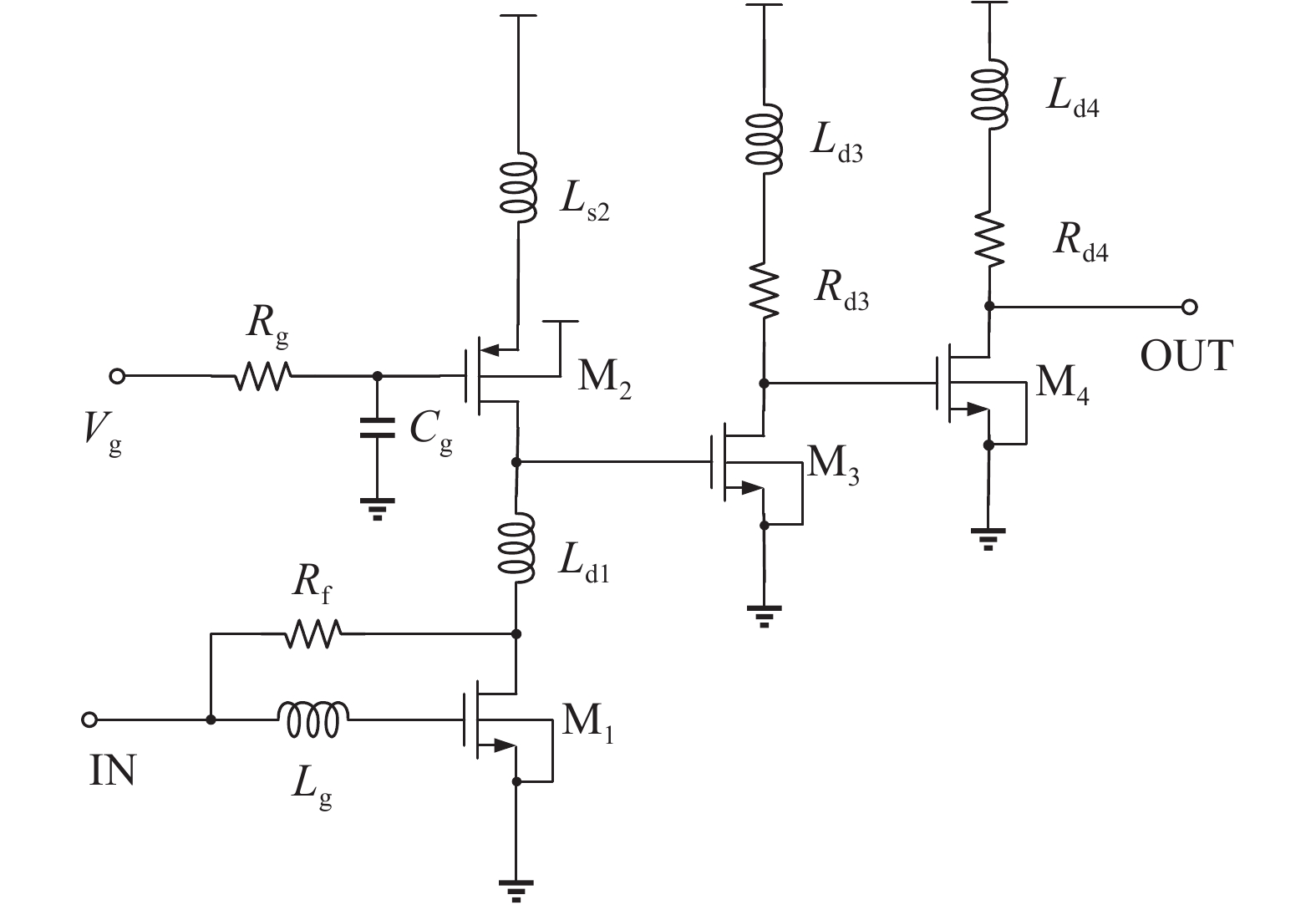
Fig. 1 shows the simplified schematic of the proposed three-stage wideband LNA. In the first stage, the feedback resistor is implemented directly between the drain of the input transistor M1 and the input node, which can ensure no bandwidth degradation and need no additional bias circuits. A PMOSFET M2 is chosen as the load so that the gate voltage of M1 and M3 can be adjusted to obtain high voltage gain over a wide range of frequencies, and it can also counteract the influence of process variation. In the second stage, the common-source amplifier is added to improve the isolation between the input and the output. The shunt peaking inductor is also used in the second stage to further enhance the bandwidth. The common-source buffer with a shunt peaking inductor is employed as the third stage to achieve wideband output matching. The signal at the former stage is directly coupled to the next stage to ensure no extra power consumption and less bandwidth degradation.

Figure  1.  Simplified schematic of the proposed wideband LNA.

To increase the bandwidth of the LNA, a number of methods are adopted in this design. Firstly, the feedback resistor Rf is connected between the drain of the input transistor and the input node, which can reduce the input quality factor (Q) and thus extend the bandwidth. Secondly, an inductor Lg placed inside the feedback loop at the gate of the input transistor is added. According to reference[8], the inductor Lg will introduce three poles in the transfer function of the voltage gain. Thirdly, the inductor shunt peaking technique has been used. The simulation result shows that the shunt peaking inductor can increase the bandwidth by 19% compared with that of no shunt peaking inductors[9]. Finally, the inductor at the drain of the input transistor is added, which can counteract some capacitance of the next stage at high frequency and increase the flexibility of the input matching.

The overall gain can be expressed as Av(s)=Av1(s) Av2(s)Av3(s) and the gain of each stage is listed below:

Av1(s)=(1gm1Rfs2Cgs1Lg+1)11+RfYL(s)gm2rds2Ls2gm2rds2Ls2+Ld1,
(1)
Av2(s)=gm3Rd3+sLd3s2Ld3Cgs4+sRd3Cgs4+1,
(2)
Av3(s)=gm4[(Rd4+sLd4)//50Ω],
(3)

where the YL(s) represents the load admittance at the drain of the M1, and can be expressed as:

YL(s)=(s2gm2rds2Ls2CL+1)(sLd1+rds1)+sgm2rds2Ls2rds1[sLd1(s2gm2rds2Ls2CL+1)+sgm2rds2Ls2].
(4)

Here, the CL represents the load capacitor of the first stage and CL = Cgs3 + Cdb2.

Input impedance matching is an important parameter in LNA design because poor matching at the receiver input will lead to significant reflections, an uncharacterized loss, and possibly voltage attenuation. In the proposed LNA, the wideband input matching is achieved by adjusting the first stage gain, the feedback resistor, the inductor at the gate of M1 and an inductor in series at the drain of the M1.

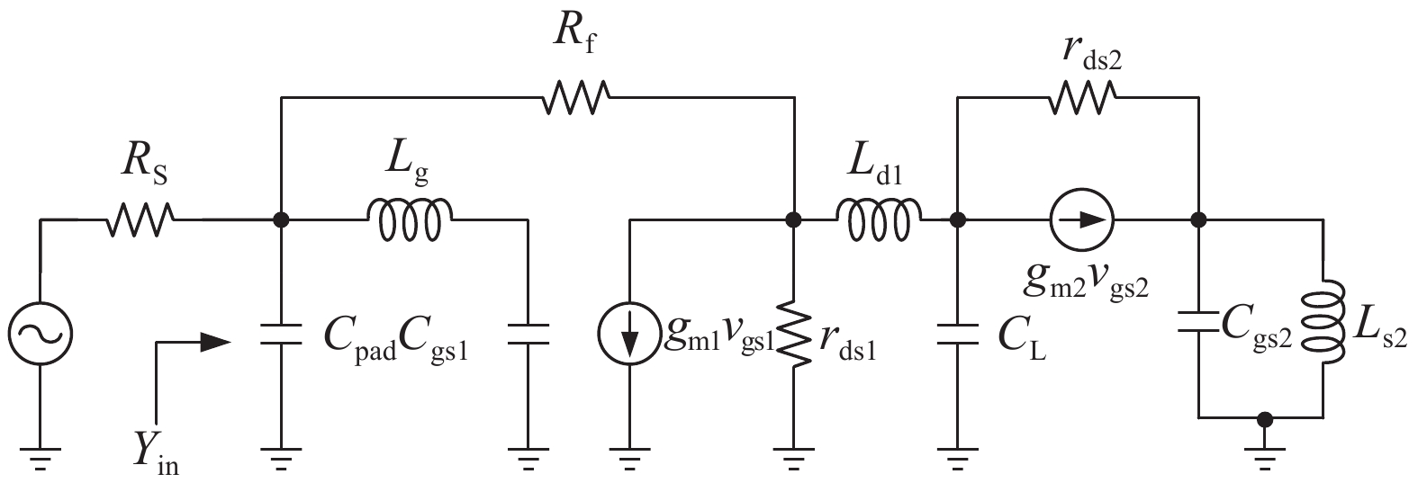
Fig. 2 shows the small signal equivalent circuit of the input network, where the capacitor Cpad represents the parasite capacitor of the input pad. The input admittance can be derived as:

Figure  2.  The small signal equivalent circuit of the input network.
Yin(s)=sCpad+sCgs1s2LgCgs1+1+gm11Rf1(s2LgCgs1+1)YL(s).
(5)

The YL(s) is given in Eq. (4).

The noise performance of the proposed LNA is mainly determined by the first stage according to the Friis’ equation. In the first stage, three primary noise sources are the noise of the input transistor M1, the noise of the loading device M2, and the noise of the feedback resistor. The noise contributed by M1 can be optimized by selecting an appropriate width. When it comes to the noise of M2, the shunt peaking inductor plays the role of source degeneration, which could suppress the noise of M2 at high frequencies. The noise factor is shown in Eq. (6).

F1+RsRf+γ1(1+ω2C2gsR2s)α1gm1Rs+γ2gdo2(1+ω2C2gsR2s)g2m1Rs(1+ω2L2s2g2m2).
(6)

The passive mixer has the great benefits of low flicker noise and high linearity with low power consumption. Therefore, it is adopted here to mitigate design tradeoff between low-frequency flicker noise and various IF bandwidth requirements.

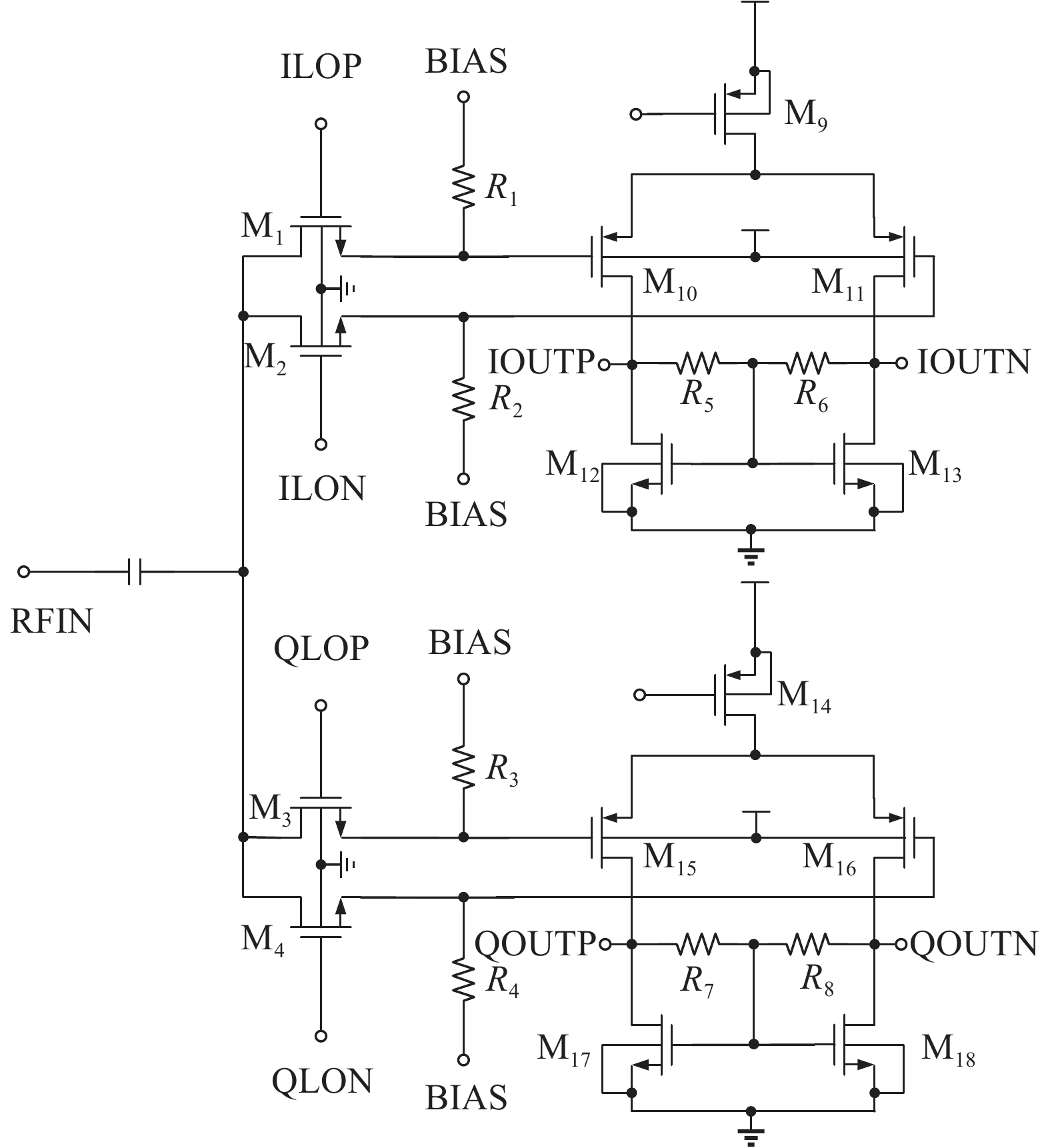
As shown in Fig. 3, the proposed mixer is composed of passive switches and IF amplifiers. The passive switches, as biased in the on-overlap region for linearity performance, are driven by the local oscillator (LO) chains. The size of the passive switches needs to be selected properly, because the white noise of the mixer depends on the channel resistance of the MOSFET, which are on at a given time. The IF amplifier can not only provide suitable gain to compensate the loss in the passive mixer but also filter the high frequency signal.

Figure  3.  The schematic of the proposed passive mixer.

The differential conversion gain of I/Q output is given by

Aconversion=2πgm10(rds12//R5).
(7)

Here, the parameters of the RF transistors and resistors satisfy gm10 = gm11 = gm15 = gm16, rds12 = rds13 = rds17 = rds18, and R5 = R6 = R7 = R8.

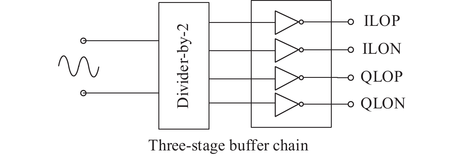
In the LO chain, as shown in Fig. 4, a divide-by-2 divider is used to generate the quadrature signal. After the divider, the LO signal is distributed to a three-stage buffer chain. The chain includes two cascade differential amplifiers as the first two stages and inverter-type drivers as the third stage for maximal signal swing.

Figure  4.  The schematic of the proposed LO chain.

Based on the broadband LNA and voltage-driven passive mixer mentioned above, the broadband RF receiver front-end chip was fabricated in CMOS process, as shown in Fig. 5. It occupies an area of 1.67 × 1.08 mm2, including pads and guard rings. The chip is mounted on a printed circuit board (PCB) with chip-on-board technique for measurement.

Figure  5.  Microphotograph of the wideband RF front-end chip.

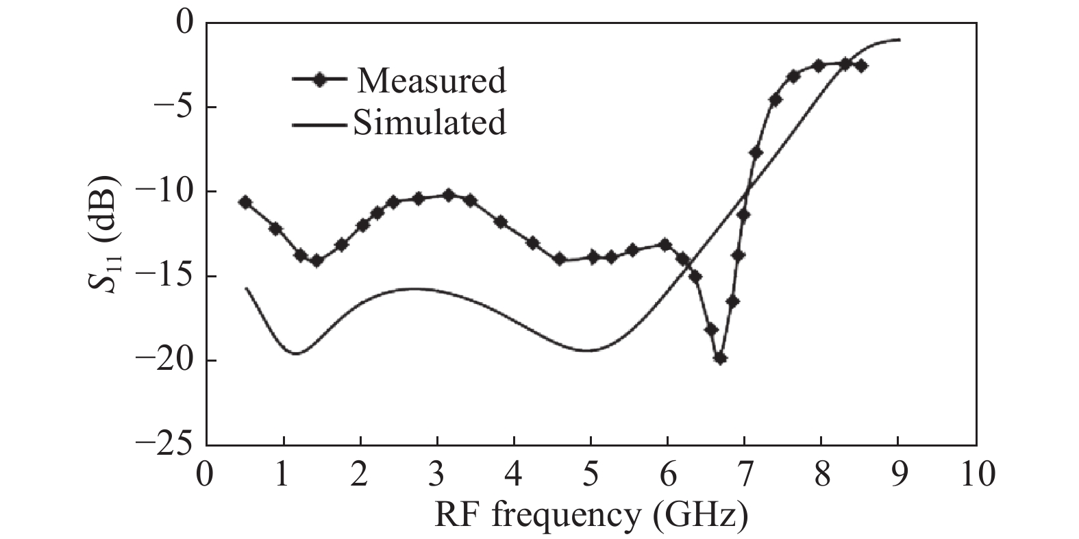
The measured and simulated results are given below. The measured results introduce some loss due to the bonding. Fig. 6 presents the measurement result of S11 from 0.5 to 8.5 GHz. The measured S11 is better than −10 dB from 700 MHz to 7 GHz and reaches the best input impedance matching of −20 dB at about 6.8 GHz.

Figure  6.  Measured S11.

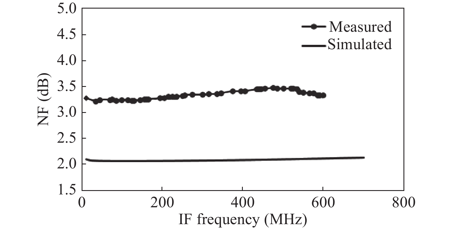
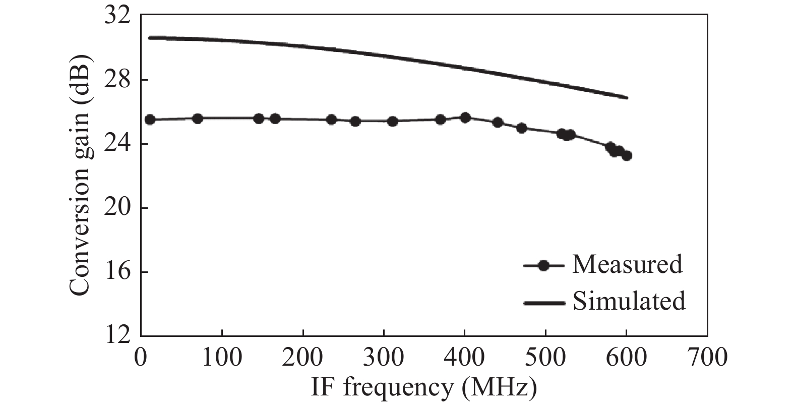
As depicted in Fig. 7, NF is less than 3.5 dB when the IF frequency is from 10 to 600 MHz and achieves a minimum value of 3.2 dB at 70 MHz when the LO is 2.5 GHz. In Fig. 8, the conversion gain is given. The maximum conversion gain reaches 26 dB and the IF 3 dB-bandwidth is larger than 500 MHz. This chip is reconfigurable from 0.7 to 7 GHz. The conversion gain under different LO frequencies is shown in Fig. 9.

Figure  7.  Measured NF (fLO = 2.5 GHz).
Figure  8.  Measured conversion gain (fLO = 2.5 GHz).
Figure  9.  Measured conversion gain under different LOs (fLO1 = 2.5 GHz, fLO2 = 5 GHz, fLO3 = 7 GHz).

Table 1 lists the major specifications of various wireless communication standards along with the performances of this work. The performance summary and the comparison with recently published results are listed in Table 2. According to Table 2, this work achieves wider RF and IF bandwidths and lower noise.

Table  1.  Specification of various wireless communication standards and comparisons with this work.
Parameter LTE 802.11g 802.11ac This work
Frequency (GHz) 0.9, 1.8, 1.9, 2.0, 2.4, 2.5, 2.6 2.4 5.8 0.7–7
NF (dB) 5 14.8 14 3.5
IIP3 (dBm) −20 −22.5 −24 −19.5
P1dB (dBm) −25 −26 −26 −23
Channel BW (MHz) 20 22 160 600
DownLoad: CSV  | Show Table
Table  2.  Performance comparisons with recently published RF receiver front-end.
Parameter RF band (GHz) IF Bandwidth (MHz) Gain (dB) NF(DSB) (dB) S11 (dB) Area (mm2) Supply (V)
This work 0.7–7 600 26 3.2–3.5 < −10 1.8 1.2
Ref. [1] 0.6–3 0.8–12 48–42 3 < −8 1.5 1.2
Ref. [10] 0.05–2.5 0.3–20 22–30 2.7–4.5 1.36 1.8
Ref. [11] 0.9–2.6 35–70 33.5 5.3 < −10 2.75* 1.8
Ref. [12] 0.9–5.8 22–25 < 4 < −10 4.2 1.2
* The area of whole receiver.
DownLoad: CSV  | Show Table

In this paper, the design and measurement results of a wideband receiver front-end SoC in CMOS technology have been presented. The proposed single-ended LNA adopts a shunt-peaking technique to boost the bandwidth, resulting in excellent overall performances throughout the spectrum ranging from 0.7 to 7 GHz. Based on this resistive-feedback broadband LNA, the wideband RF receiver front-end SoC can cover multiple communication applications. Experimental results validate that the wideband receiver RF front-end achieves good input impedance matching, high gain, low noise and wide IF bandwidth.


[1]
Wang X, Sturm J, Yan N, et al. 0.6–3-GHz wideband receiver RF front-end with a feedforward noise and distortion cancellation resistive-feedback LNA. IEEE Trans Microwave Theory Tech, 2012, 60(2): 387 doi: 10.1109/TMTT.2011.2176138
[2]
Zhou H M, Zhang Y, Yu Y, et al. Analysis and design of a 3.1-10.6 GHz wideband low-noise amplifier using resistive feedback. IEEE International Conference on Ubiquitous Wireless Broadband (ICUWB), 2016: 1
[3]
Cho K F, Wang S. A 0.4–5.3 GHz wideband LNA using resistive feedback topology. IEEE MTT-S International Conference on Numerical Electromagnetic and Multiphysics Modeling and Optimization (NEMO), 2016: 1
[4]
Zhang X G, Yang L J, Huang F Y. A 0.3–6 GHz broadband noise cancelling low noise amplifier. International Conference on Integrated Circuits and Microsystems (ICICM), 2016: 144
[5]
Morena-Álvarez-Palencia C D L, Burgos-García M. Broadband RF front-end based on the six-port network architecture for software defined radio. 2010 Milcom Military Communications Conference, 2010: 2137
[6]
Adiseno I, Ismail M, Olsson H. A wide-band RF front-end for multiband multistandard high-linearity low-IF wireless receivers. IEEE J Solid-State Circuits, 2002, 37(9): 1162
[7]
Wang C, Li Z Q, Li Q, et al. A broadband 47–67 GHz LNA with 17.3 dB gain in 65-nm CMOS. J Semicond, 2015, 36(10): 105010 doi: 10.1088/1674-4926/36/10/105010
[8]
Chang T, Chen J, Rigge L A, et al. ESD-protected wideband CMOS LNAs using modified resistive feedback techniques with chip-on-board packaging. IEEE Trans Microwave Theory Tech, 2008, 56(8): 1817 doi: 10.1109/TMTT.2008.927301
[9]
Chen M Q, Lin J S. A 0.1–20 GHz low-power self-biased resistive-feedback LNA in 90 nm digital CMOS. IEEE Microwave Wireless Compon Lett, 2009, 19(5): 323 doi: 10.1109/LMWC.2009.2017608
[10]
Liu L, Zhang K, Ren Z, et al. 0.05–2.5 GHz wideband RF front-end exploiting noise cancellation and multi-gated transistors. IEEE Asia-Pacific Microwave Conference, 2015: 1
[11]
Qiu L, Liu S, Zhang Y, et al. A 0.9–2.6 GHz cognitive radio receiver with spread spectrum frequency synthesizer for spectrum sensing. IEEE Sens J, 2017, 17(22): 7569 doi: 10.1109/JSEN.2017.2760339
[12]
Wu L, Ng A W L, Zheng S, et al. A 0.9–5.8-GHz software-defined receiver RF front-end with transformer-based current-gain boosting and harmonic rejection calibration. IEEE Trans Very Large Scale Integr (VLSI) Syst, 2017, 25(8): 2371 doi: 10.1109/TVLSI.2017.2695719
Fig. 1.  Simplified schematic of the proposed wideband LNA.

Fig. 2.  The small signal equivalent circuit of the input network.

Fig. 3.  The schematic of the proposed passive mixer.

Fig. 4.  The schematic of the proposed LO chain.

Fig. 5.  Microphotograph of the wideband RF front-end chip.

Fig. 6.  Measured S11.

Fig. 7.  Measured NF (fLO = 2.5 GHz).

Fig. 8.  Measured conversion gain (fLO = 2.5 GHz).

Fig. 9.  Measured conversion gain under different LOs (fLO1 = 2.5 GHz, fLO2 = 5 GHz, fLO3 = 7 GHz).

Table 1.   Specification of various wireless communication standards and comparisons with this work.

Parameter LTE 802.11g 802.11ac This work
Frequency (GHz) 0.9, 1.8, 1.9, 2.0, 2.4, 2.5, 2.6 2.4 5.8 0.7–7
NF (dB) 5 14.8 14 3.5
IIP3 (dBm) −20 −22.5 −24 −19.5
P1dB (dBm) −25 −26 −26 −23
Channel BW (MHz) 20 22 160 600
DownLoad: CSV

Table 2.   Performance comparisons with recently published RF receiver front-end.

Parameter RF band (GHz) IF Bandwidth (MHz) Gain (dB) NF(DSB) (dB) S11 (dB) Area (mm2) Supply (V)
This work 0.7–7 600 26 3.2–3.5 < −10 1.8 1.2
Ref. [1] 0.6–3 0.8–12 48–42 3 < −8 1.5 1.2
Ref. [10] 0.05–2.5 0.3–20 22–30 2.7–4.5 1.36 1.8
Ref. [11] 0.9–2.6 35–70 33.5 5.3 < −10 2.75* 1.8
Ref. [12] 0.9–5.8 22–25 < 4 < −10 4.2 1.2
* The area of whole receiver.
DownLoad: CSV
[1]
Wang X, Sturm J, Yan N, et al. 0.6–3-GHz wideband receiver RF front-end with a feedforward noise and distortion cancellation resistive-feedback LNA. IEEE Trans Microwave Theory Tech, 2012, 60(2): 387 doi: 10.1109/TMTT.2011.2176138
[2]
Zhou H M, Zhang Y, Yu Y, et al. Analysis and design of a 3.1-10.6 GHz wideband low-noise amplifier using resistive feedback. IEEE International Conference on Ubiquitous Wireless Broadband (ICUWB), 2016: 1
[3]
Cho K F, Wang S. A 0.4–5.3 GHz wideband LNA using resistive feedback topology. IEEE MTT-S International Conference on Numerical Electromagnetic and Multiphysics Modeling and Optimization (NEMO), 2016: 1
[4]
Zhang X G, Yang L J, Huang F Y. A 0.3–6 GHz broadband noise cancelling low noise amplifier. International Conference on Integrated Circuits and Microsystems (ICICM), 2016: 144
[5]
Morena-Álvarez-Palencia C D L, Burgos-García M. Broadband RF front-end based on the six-port network architecture for software defined radio. 2010 Milcom Military Communications Conference, 2010: 2137
[6]
Adiseno I, Ismail M, Olsson H. A wide-band RF front-end for multiband multistandard high-linearity low-IF wireless receivers. IEEE J Solid-State Circuits, 2002, 37(9): 1162
[7]
Wang C, Li Z Q, Li Q, et al. A broadband 47–67 GHz LNA with 17.3 dB gain in 65-nm CMOS. J Semicond, 2015, 36(10): 105010 doi: 10.1088/1674-4926/36/10/105010
[8]
Chang T, Chen J, Rigge L A, et al. ESD-protected wideband CMOS LNAs using modified resistive feedback techniques with chip-on-board packaging. IEEE Trans Microwave Theory Tech, 2008, 56(8): 1817 doi: 10.1109/TMTT.2008.927301
[9]
Chen M Q, Lin J S. A 0.1–20 GHz low-power self-biased resistive-feedback LNA in 90 nm digital CMOS. IEEE Microwave Wireless Compon Lett, 2009, 19(5): 323 doi: 10.1109/LMWC.2009.2017608
[10]
Liu L, Zhang K, Ren Z, et al. 0.05–2.5 GHz wideband RF front-end exploiting noise cancellation and multi-gated transistors. IEEE Asia-Pacific Microwave Conference, 2015: 1
[11]
Qiu L, Liu S, Zhang Y, et al. A 0.9–2.6 GHz cognitive radio receiver with spread spectrum frequency synthesizer for spectrum sensing. IEEE Sens J, 2017, 17(22): 7569 doi: 10.1109/JSEN.2017.2760339
[12]
Wu L, Ng A W L, Zheng S, et al. A 0.9–5.8-GHz software-defined receiver RF front-end with transformer-based current-gain boosting and harmonic rejection calibration. IEEE Trans Very Large Scale Integr (VLSI) Syst, 2017, 25(8): 2371 doi: 10.1109/TVLSI.2017.2695719
  • Search

    Advanced Search >>

    GET CITATION

    shu

    Export: BibTex EndNote

    Article Metrics

    Article views: 4232 Times PDF downloads: 104 Times Cited by: 0 Times

    History

    Received: 25 July 2017 Revised: 26 March 2018 Online: Uncorrected proof: 16 May 2018Published: 09 August 2018

    Catalog

      Email This Article

      User name:
      Email:*请输入正确邮箱
      Code:*验证码错误
      Youming Zhang, Lijuan Yang, Fengyi Huang, Nan Jiang, Xuegang Zhang. A 0.7–7 GHz wideband reconfigurable receiver RF front-end in CMOS[J]. Journal of Semiconductors, 2018, 39(8): 085003. doi: 10.1088/1674-4926/39/8/085003 ****Y M Zhang, L J Yang, F Y Huang, N Jiang, X G Zhang, A 0.7–7 GHz wideband reconfigurable receiver RF front-end in CMOS[J]. J. Semicond., 2018, 39(8): 085003. doi: 10.1088/1674-4926/39/8/085003.
      Citation:
      Youming Zhang, Lijuan Yang, Fengyi Huang, Nan Jiang, Xuegang Zhang. A 0.7–7 GHz wideband reconfigurable receiver RF front-end in CMOS[J]. Journal of Semiconductors, 2018, 39(8): 085003. doi: 10.1088/1674-4926/39/8/085003 ****
      Y M Zhang, L J Yang, F Y Huang, N Jiang, X G Zhang, A 0.7–7 GHz wideband reconfigurable receiver RF front-end in CMOS[J]. J. Semicond., 2018, 39(8): 085003. doi: 10.1088/1674-4926/39/8/085003.

      A 0.7–7 GHz wideband reconfigurable receiver RF front-end in CMOS

      DOI: 10.1088/1674-4926/39/8/085003
      More Information
      • Corresponding author: Email: fyhuang@seu.edu.cn
      • Received Date: 2017-07-25
      • Revised Date: 2018-03-26
      • Published Date: 2018-08-01

      Catalog

        /

        DownLoad:  Full-Size Img  PowerPoint
        Return
        Return