


Fig. 1.
(Color online) Schematic of the band alignment for T2SLs InAs / GaSb, where CBO is conduction band offset.
SEMICONDUCTOR DEVICES
Tetiana Manyk, Klaudia Hackiewicz, Jaroslaw Rutkowski and Piotr Martyniuk
Corresponding author: Tetiana Manyk, tetjana.manyk@wat.edu.pl
Abstract: The investigation of the interband type-II superlattice InAs/GaSb cascade photodetector in the temperature range of 320–380 K is presented. The article is devoted to the theoretical modeling of the cascade detector characteristics by the use of the SimuApsys platform and the 4-band model (k∙p 8 × 8 method). The obtained theoretical characteristics are comparable with experimentally measured ones, suggesting that transport in the absorber is determined by the dynamics of intrinsic carriers and by their lifetime. An overlap equal to 120 meV was used in calculations and a correction term in the " non-common atom” model Hxy = 700 meV was added to the Hamiltonian. The electron and hole effective masses from dispersion curves were estimated and absorption coefficient α was calculated. Based on the simulation detectivity, D* characteristics in the temperature range 320–380 K were calculated. The simulated theoretical characteristics at 320 K are comparable to experimentally measured ones, however at higher temperatures, the experimental value of D* does not reach the theoretical values due to the low resistance of the device and short diffusion length.
Keywords: interband cascade photodetectors, type-II superlattice, infrared detectors
| [1] |
Sudha M, Chennupati J. III–V compound SC for optoelectronic devices. Mater Today, 2009, 12(4): 22 doi: 10.1016/S1369-7021(09)70110-5
|
| [2] |
Smith D L, Mailhiot C. Proposal for strained type II superlattice infrared detectors. J Appl Phys, 1987, 62(6): 2545 doi: 10.1063/1.339468
|
| [3] |
Rogalski A, Kopytko M, Martyniuk P. InAs/GaSb type-II superlattice infrared detectors: three decades of development. Proc SPIE, 2017: 1017715
|
| [4] |
Tian Z, Hinkey R T, Yang R Q, et al. Interband cascade infrared photodetectors with enhanced electron barriers and p-type superlattice absorbers. J Appl Phys, 2012, 111(2): 024510 doi: 10.1063/1.3678003
|
| [5] |
Hinkey R T, Yang R Q. Theory of multiple-stage interband photovoltaic devices and ultimate performance limit comparison of multiple-stage and single-stage interband infrared detectors. J Appl Phys, 2013, 114(10): 104506 doi: 10.1063/1.4820394
|
| [6] |
Hackiewicz K, Martyniuk P, Rutkowski J, et al. Dark current simulation in interband cascade photodetectors operating in room temperature. Proc SPIE, 2017: 104550
|
| [7] |
Lestrade M, Li Z Q, Li Z S. Finite difference k∙p modeling of type II MQWs. Opt Quantum Electron, 2014, 46(10): 1345 doi: 10.1007/s11082-014-9881-7
|
| [8] |
Vurgaftman I, Meyer J R, Ram-Mohan L R. Band parameters for III–V compound semiconductors and their alloys. J Appl Phys, 2001, 89(11): 5815 doi: 10.1063/1.1368156
|
| [9] |
Karazhanov S Z. Ab initio studies of the band parameters of III–V and II–VI zinc-blende semiconductors. Semiconductors, 2005, 39(2): 161 doi: 10.1134/1.1864192
|
| [10] |
Gautam N, Myers S, Barve A V, et al. High operating temperature interband cascade midwave infrared detector based on type-II InAs/GaSb strained layer superlattice. Appl Phys Lett, 2012, 101(2): 021106 doi: 10.1063/1.4733660
|
| [11] |
Livneh Y, Klipstein P C, Klin O, et al. k∙p model for the energy dispersions and absorption spectra of InAs/GaSb type-II superlattices. Phys Rev B, 2012, 86: 235311 doi: 10.1103/PhysRevB.86.235311
|
| [12] |
Qiao P F, Mou S, Chuang S L. Electronic band structures and optical properties of type-II superlattice photodetectors with interfacial effect. Opt Express, 2012, 20(3): 2319 doi: 10.1364/OE.20.002319
|
| [13] |
Lei L, Li L, Ye H, et al. Long wavelength interband cascade infrared photodetectors operating at high temperatures. J Appl Phys, 2016, 120(19): 193102 doi: 10.1063/1.4967915
|
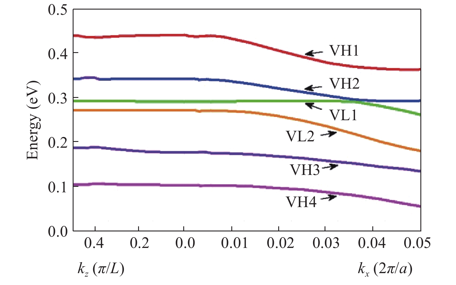

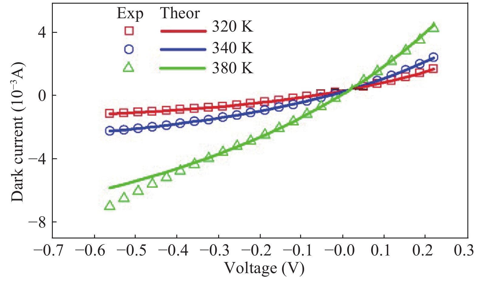

Table 1. Band structure parameters for the InAs and GaSb.
| Parameter | Symbol | Material | |
| InAs | GaSb | ||
Lattice constant A = a0 +


|
a (Å) | 6.0583 + 2.74 × 10⁻⁵ × (T − 300) | 6.0959 + 4.72 × 10⁻⁵ × (T − 300) |
Band gap Eg = Eg0 −


|


|
0.276 × 10⁻³ | 0.417 × 10⁻³ |
| β0 (K) | 93 | 140 | |
| Eg0 (eV) | 0.417 | 0.812 | |
| Luttinger parameters | γ1 | 19.481 | 16.291 |
| γ2 | 8.428 | 6.305 | |
| γ3 | 9.171 | 7.371 | |
| Deformation potential | ac (eV) | −5.08 | −7.5 |
| av (eV) | −1.00 | −0.8 | |
| b (eV) | −1.8 | −2 | |
| Elastic constant | C11 (GPa) | 83.29 | 88.42 |
| C12 (GPa) | 45.26 | 40.26 | |
| C44 (GPa) | 39.59 | 43.22 | |
| Spin orbit energy | ΔSO (eV) | 0.39 | 0.76 |
| Effective mass |


|
0.028 | 0.035 |
| Kane potential | Ep (eV) | 14.427 | 15.726 |
 DownLoad: CSV
Table 2. Calculated band gap parameters of T2SLs InAs/GaSb.
| Temperatures (K) | VH1 (eV) | VH2 (eV) | VL1 (eV) | VL2 (eV) | VH3 (eV) | VH4 (eV) | Eg (eV) | VBO (eV) |
| 320 | 0.459 | 0.362 | 0.308 | 0.287 | 0.191 | 0.119 | 0.2 | 0.469 |
| 340 | 0.455 | 0.357 | 0.303 | 0.284 | 0.187 | 0.114 | 0.1935 | 0.463 |
| 380 | 0.447 | 0.347 | 0.294 | 0.276 | 0.179 | 0.106 | 0.1836 | 0.453 |
DownLoad: CSV
| [1] |
Sudha M, Chennupati J. III–V compound SC for optoelectronic devices. Mater Today, 2009, 12(4): 22 doi: 10.1016/S1369-7021(09)70110-5
|
| [2] |
Smith D L, Mailhiot C. Proposal for strained type II superlattice infrared detectors. J Appl Phys, 1987, 62(6): 2545 doi: 10.1063/1.339468
|
| [3] |
Rogalski A, Kopytko M, Martyniuk P. InAs/GaSb type-II superlattice infrared detectors: three decades of development. Proc SPIE, 2017: 1017715
|
| [4] |
Tian Z, Hinkey R T, Yang R Q, et al. Interband cascade infrared photodetectors with enhanced electron barriers and p-type superlattice absorbers. J Appl Phys, 2012, 111(2): 024510 doi: 10.1063/1.3678003
|
| [5] |
Hinkey R T, Yang R Q. Theory of multiple-stage interband photovoltaic devices and ultimate performance limit comparison of multiple-stage and single-stage interband infrared detectors. J Appl Phys, 2013, 114(10): 104506 doi: 10.1063/1.4820394
|
| [6] |
Hackiewicz K, Martyniuk P, Rutkowski J, et al. Dark current simulation in interband cascade photodetectors operating in room temperature. Proc SPIE, 2017: 104550
|
| [7] |
Lestrade M, Li Z Q, Li Z S. Finite difference k∙p modeling of type II MQWs. Opt Quantum Electron, 2014, 46(10): 1345 doi: 10.1007/s11082-014-9881-7
|
| [8] |
Vurgaftman I, Meyer J R, Ram-Mohan L R. Band parameters for III–V compound semiconductors and their alloys. J Appl Phys, 2001, 89(11): 5815 doi: 10.1063/1.1368156
|
| [9] |
Karazhanov S Z. Ab initio studies of the band parameters of III–V and II–VI zinc-blende semiconductors. Semiconductors, 2005, 39(2): 161 doi: 10.1134/1.1864192
|
| [10] |
Gautam N, Myers S, Barve A V, et al. High operating temperature interband cascade midwave infrared detector based on type-II InAs/GaSb strained layer superlattice. Appl Phys Lett, 2012, 101(2): 021106 doi: 10.1063/1.4733660
|
| [11] |
Livneh Y, Klipstein P C, Klin O, et al. k∙p model for the energy dispersions and absorption spectra of InAs/GaSb type-II superlattices. Phys Rev B, 2012, 86: 235311 doi: 10.1103/PhysRevB.86.235311
|
| [12] |
Qiao P F, Mou S, Chuang S L. Electronic band structures and optical properties of type-II superlattice photodetectors with interfacial effect. Opt Express, 2012, 20(3): 2319 doi: 10.1364/OE.20.002319
|
| [13] |
Lei L, Li L, Ye H, et al. Long wavelength interband cascade infrared photodetectors operating at high temperatures. J Appl Phys, 2016, 120(19): 193102 doi: 10.1063/1.4967915
|


Article views: 4973 Times PDF downloads: 81 Times Cited by: 0 Times
Received: 24 January 2018 Revised: 02 March 2018 Online: Uncorrected proof: 17 May 2018Accepted Manuscript: 05 July 2018Published: 01 September 2018
| Citation: |
Tetiana Manyk, Klaudia Hackiewicz, Jaroslaw Rutkowski, Piotr Martyniuk. Theoretical simulation of T2SLs InAs/GaSb cascade photodetector for HOT condition[J]. Journal of Semiconductors, 2018, 39(9): 094004. doi: 10.1088/1674-4926/39/9/094004
****
T Manyk, K Hackiewicz, J Rutkowski, P Martyniuk, Theoretical simulation of T2SLs InAs/GaSb cascade photodetector for HOT condition[J]. J. Semicond., 2018, 39(9): 094004. doi: 10.1088/1674-4926/39/9/094004.

|
| [1] |
Sudha M, Chennupati J. III–V compound SC for optoelectronic devices. Mater Today, 2009, 12(4): 22 doi: 10.1016/S1369-7021(09)70110-5
|
| [2] |
Smith D L, Mailhiot C. Proposal for strained type II superlattice infrared detectors. J Appl Phys, 1987, 62(6): 2545 doi: 10.1063/1.339468
|
| [3] |
Rogalski A, Kopytko M, Martyniuk P. InAs/GaSb type-II superlattice infrared detectors: three decades of development. Proc SPIE, 2017: 1017715
|
| [4] |
Tian Z, Hinkey R T, Yang R Q, et al. Interband cascade infrared photodetectors with enhanced electron barriers and p-type superlattice absorbers. J Appl Phys, 2012, 111(2): 024510 doi: 10.1063/1.3678003
|
| [5] |
Hinkey R T, Yang R Q. Theory of multiple-stage interband photovoltaic devices and ultimate performance limit comparison of multiple-stage and single-stage interband infrared detectors. J Appl Phys, 2013, 114(10): 104506 doi: 10.1063/1.4820394
|
| [6] |
Hackiewicz K, Martyniuk P, Rutkowski J, et al. Dark current simulation in interband cascade photodetectors operating in room temperature. Proc SPIE, 2017: 104550
|
| [7] |
Lestrade M, Li Z Q, Li Z S. Finite difference k∙p modeling of type II MQWs. Opt Quantum Electron, 2014, 46(10): 1345 doi: 10.1007/s11082-014-9881-7
|
| [8] |
Vurgaftman I, Meyer J R, Ram-Mohan L R. Band parameters for III–V compound semiconductors and their alloys. J Appl Phys, 2001, 89(11): 5815 doi: 10.1063/1.1368156
|
| [9] |
Karazhanov S Z. Ab initio studies of the band parameters of III–V and II–VI zinc-blende semiconductors. Semiconductors, 2005, 39(2): 161 doi: 10.1134/1.1864192
|
| [10] |
Gautam N, Myers S, Barve A V, et al. High operating temperature interband cascade midwave infrared detector based on type-II InAs/GaSb strained layer superlattice. Appl Phys Lett, 2012, 101(2): 021106 doi: 10.1063/1.4733660
|
| [11] |
Livneh Y, Klipstein P C, Klin O, et al. k∙p model for the energy dispersions and absorption spectra of InAs/GaSb type-II superlattices. Phys Rev B, 2012, 86: 235311 doi: 10.1103/PhysRevB.86.235311
|
| [12] |
Qiao P F, Mou S, Chuang S L. Electronic band structures and optical properties of type-II superlattice photodetectors with interfacial effect. Opt Express, 2012, 20(3): 2319 doi: 10.1364/OE.20.002319
|
| [13] |
Lei L, Li L, Ye H, et al. Long wavelength interband cascade infrared photodetectors operating at high temperatures. J Appl Phys, 2016, 120(19): 193102 doi: 10.1063/1.4967915
|

 WeChat ID
Journal of Semiconductors © 2017 All Rights Reserved 京ICP备05085259号-2


