| Citation: |
Xingye Zhou, Xin Tan, Yuangang Wang, Xubo Song, Peng Xu, Guodong Gu, Yuanjie Lü, Zhihong Feng. Coeffect of trapping behaviors on the performance of GaN-based devices[J]. Journal of Semiconductors, 2018, 39(9): 094007. doi: 10.1088/1674-4926/39/9/094007
****
X Y Zhou, X Tan, Y G Wang, X B Song, P Xu, G D Gu, Y Lü, Z H Feng, Coeffect of trapping behaviors on the performance of GaN-based devices[J]. J. Semicond., 2018, 39(9): 094007. doi: 10.1088/1674-4926/39/9/094007.
|
Coeffect of trapping behaviors on the performance of GaN-based devices
DOI: 10.1088/1674-4926/39/9/094007
More Information
-
Abstract
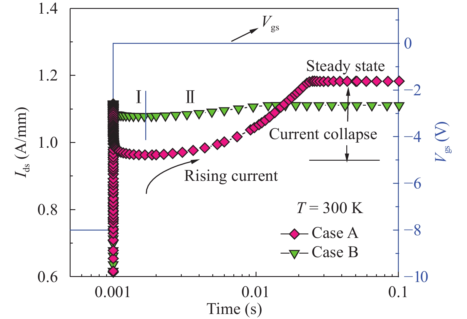
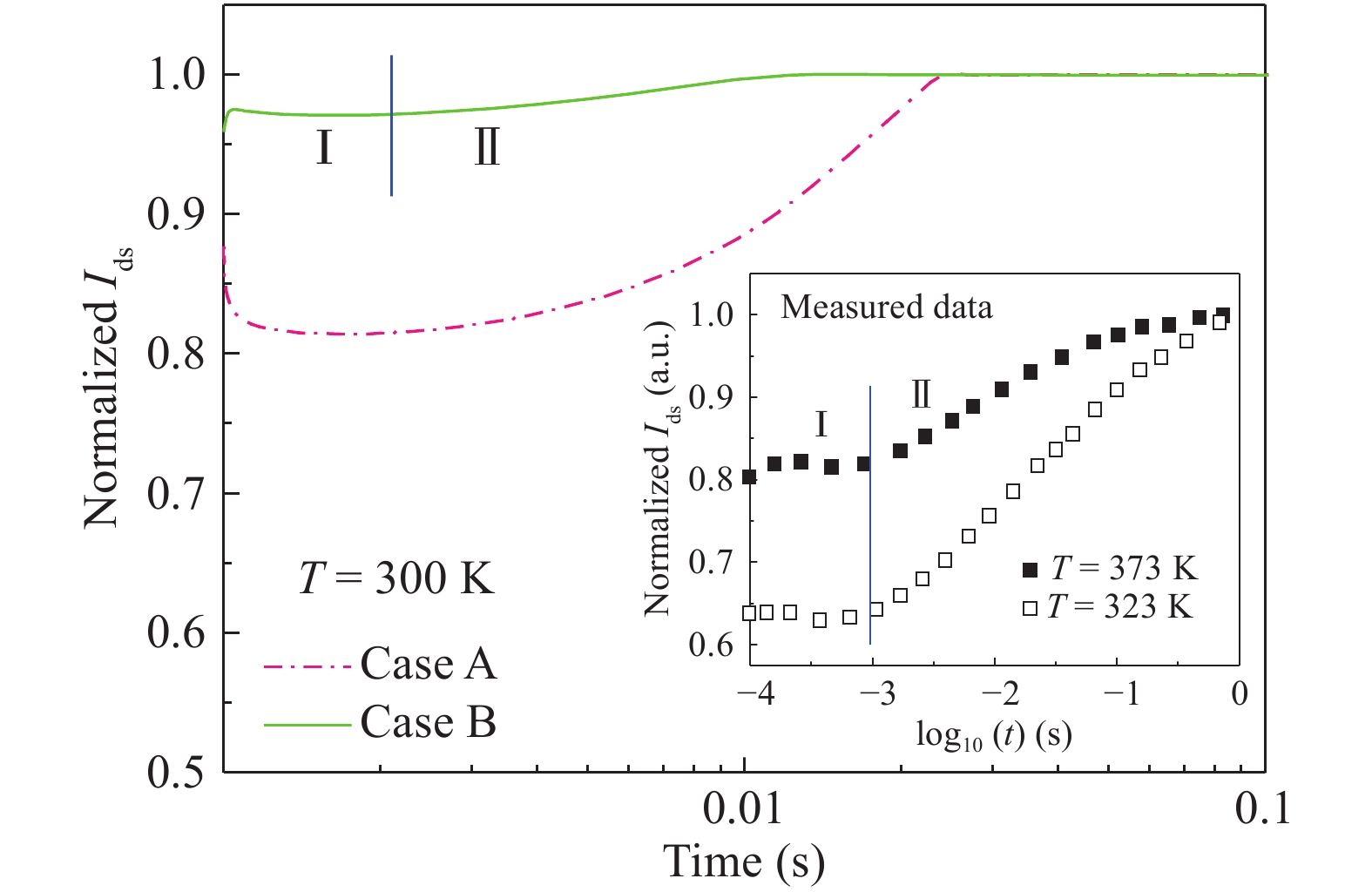
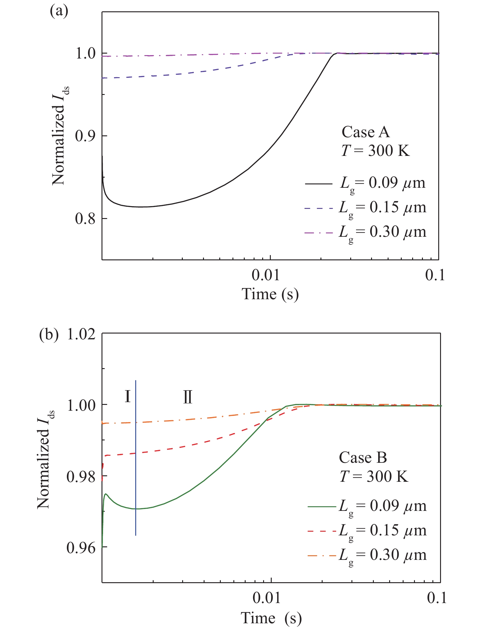
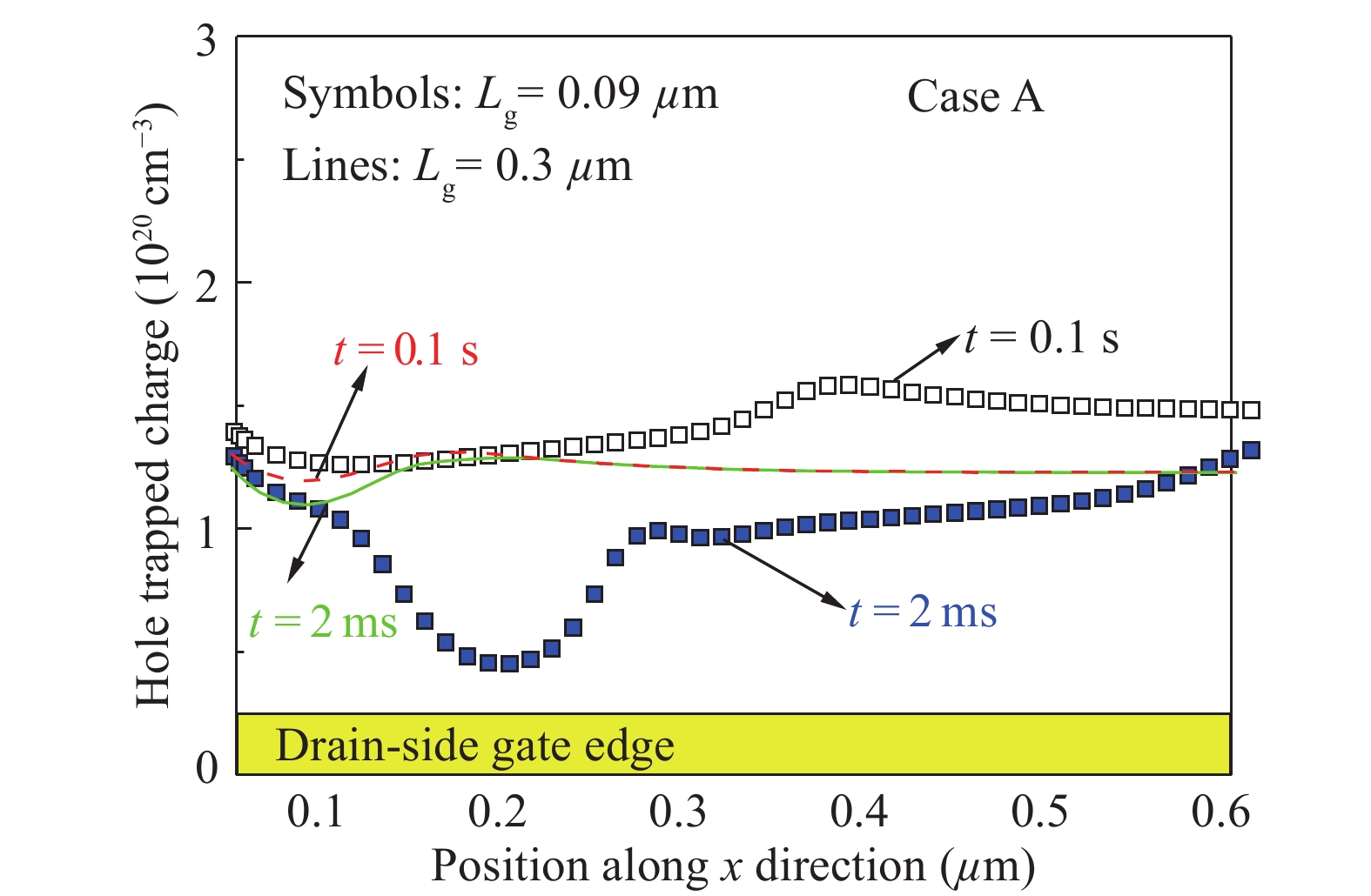
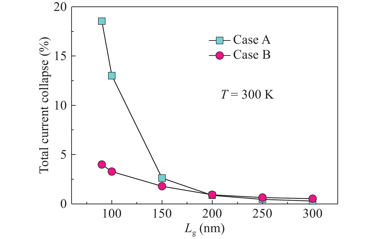
Trap-induced current collapse has become one of the critical issues hindering the improvement of GaN-based microwave power devices. It is difficult to study the behavior of each trapping effect separately with the experimental measurement. Transient simulation is a useful technique for analyzing the mechanism of current collapse. In this paper, the coeffect of surface- and bulk-trapping behaviors on the performance of AlGaN/GaN HEMTs is investigated based on the two-dimensional (2D) transient simulation. In addition, the mechanism of trapping effects is analyzed from the aspect of device physics. Two simulation models with different types of traps are used for comparison, and the simulated results reproduced the experimental measured data. It is found that the final steady-state current decreases when both the surface and bulk traps are taken into account in the model. However, contrary to the expectation, the total current collapse is dramatically reduced (e.g. from 18% to 4% for the 90 nm gate-length device). The results suggest that the surface-related current collapse of GaN-based HEMTs may be mitigated in some degree due to the participation of bulk traps with short time constant. The work in this paper will be helpful for further optimization design of material and device structures.-
Keywords:
- GaN-based HEMT,
- device physics,
- trapping effect,
- transient simulation
-
References
[1] Pengelly R S, Wood S M, Milligan J W, et al. A review of GaN on SiC high electron-mobility power transistors and MMICs. IEEE Trans Microw Theory Tech, 2012, 60(6): 1764 doi: 10.1109/TMTT.2012.2187535[2] Klein P B, Binari S C, Ikossi-Anastasiou K, et al. Investigation of traps producing current collapse in AlGaN/GaN high electron mobility transistors. Electron Lett, 2001, 37(10): 661 doi: 10.1049/el:20010434[3] Meneghesso G, Verzellesi G, Pierobon R, et al. Surface-related drain current dispersion effects in AlGaN–GaN HEMTs. IEEE Trans Electron Devices, 2004, 51(10): 1554 doi: 10.1109/TED.2004.835025[4] Tirado J M, Sanchez-Rojas J L, Izpura J I. Trapping effects in the transient response of AlGaN/GaN HEMT devices. IEEE Trans Electron Devices, 2007, 54(3): 410 doi: 10.1109/TED.2006.890592[5] Zhang W, Zhang Y, Mao W, et al. Influence of the interface acceptor-like traps on the transient response of AlGaN/GaN HEMTs. IEEE Electron Device Lett, 2013, 34(1): 45 doi: 10.1109/LED.2012.2227235[6] Braga N, Mickevicius R. Simulation of gate lag and current collapse in gallium nitridefield-effect transistors. Appl Phys Lett, 2004, 85(20): 4780 doi: 10.1063/1.1823018[7] Chini A, Lecce V D, Esposto M, et al. Evaluation and numerical simulations of GaN HEMTs electrical degradation. IEEE Electron Device Lett, 2009, 30(10): 1021 doi: 10.1109/LED.2009.2029875[8] Hu W, Chen X, Yin F, et al. Two-dimensional transient simulations of drain lag and current collapse in GaN-based high-electron-mobility transistors. J Appl Phys, 2009, 105: 084502 doi: 10.1063/1.3106603[9] Zhou X, Feng Z, Wang L, et al. Impact of bulk traps in GaN buffer on the gate-lag transient characteristics of AlGaN/GaN HEMTs. Solid-State Electron, 2014, 100: 15 doi: 10.1016/j.sse.2014.06.040[10] Zhou X, Feng Z, Wang Y, et al. Transient simulation of AlGaN/GaN HEMT including trapping and thermal effects. The 12th IEEE International Conference on Solid-State and Integrated Circuit Technology, 2014: 1079[11] Yang L, Hu G, Hao Y, et al. Electric-stress reliability and current collapse of different thickness SiNx passivated AlGaN/GaN high electron mobility transistors. Chin Phys B, 2010, 19: 047301 doi: 10.1088/1674-1056/19/4/047301[12] Pu Y, Pang L, Chen X, et al. Dispersion effect on the current voltage characteristic of AlGaN/GaN high electron mobility transistors. Chin Phys B, 2011, 20: 097305 doi: 10.1088/1674-1056/20/9/097305[13] Marso M, Wolter M, Javorka P, et al. Investigation of buffer traps in an AlGaN/GaN/Si high electron mobility transistor by back gating current deep level transient spectroscopy. Appl Phys Lett, 2003, 82(4): 633 doi: 10.1063/1.1540239[14] Meneghini M, Ronchi N, Stocco A, et al. Investigation of trapping and hot-electron effects in GaN HEMTs by means of a combined electrooptical method. IEEE Trans Electron Devices, 2011, 58(9): 2996 doi: 10.1109/TED.2011.2160547[15] Bisi D, Meneghini M, Santi C, et al. Deep-level characterization in GaN HEMTs-part I: advantages and limitations of drain current transient measurements. IEEE Trans Electron Devices, 2013, 60(3): 3166[16] Miccoli C, Martino V C, Reina S, et al. Trapping and thermal effects analysis for AlGaN/GaN HEMTs by means of TCAD simulations. IEEE Electron Device Lett, 2013, 34(9): 1121 doi: 10.1109/LED.2013.2274326[17] Zhou X, Feng Z, Lv Y, et al. Dependency of current collapse on the device structure of GaN-based HEMTs. The 11th IEEE International Conference on ASIC, 2015: 303[18] Wang M, Yan D, Zhang C, et al. Investigation of surface- and buffer-induced current collapse in GaN high-electron mobility transistors using a soft switched pulsed I−V measurement. IEEE Electron Device Lett, 2014, 35(11): 1094 doi: 10.1109/LED.2014.2356720[19] Zhang C, Wang M, Xie B, et al. Temperature dependence of the surface- and buffer-induced current collapse in GaN high-electron mobility transistors on Si substrate. IEEE Trans Electron Devices, 2015, 62(8): 2475 doi: 10.1109/TED.2015.2446504[20] Ambacher O, Smart J, Shealy J, et al. Two-dimensional electron gases induced by spontaneous and piezoelectric polarization charges in N- and Ga-face AlGaN/GaN heterostructures. J Appl Phys, 1999, 85(6): 3222 doi: 10.1063/1.369664[21] SmorchkovaI P, Elsass C R, Ibbetson J P, et al. Polarization-induced charge and electron mobility in AlGaN/GaN heterostructures grown by plasma-assisted molecular-beam epitaxy. J Appl Phys, 1999, 86(8): 4520 doi: 10.1063/1.371396 -
Proportional views


 DownLoad:
