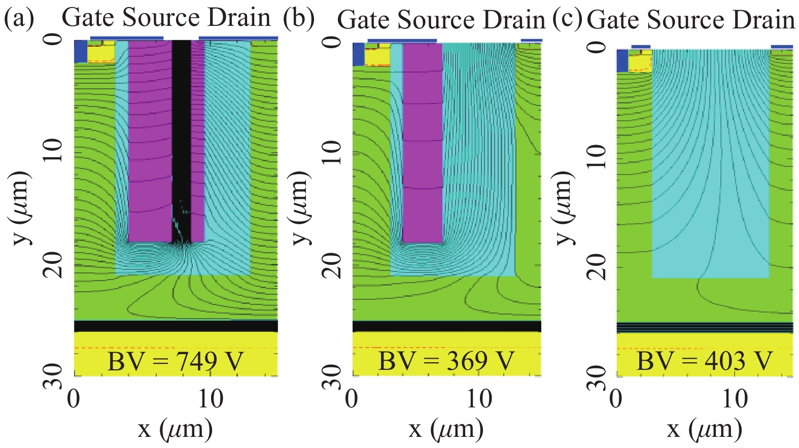
J. Semicond. > 2018, Volume 39 > Issue 9 > 094009

SEMICONDUCTOR DEVICES

An improved SOI trench LDMOST with double vertical high-k insulator pillars

Huan Li, Haimeng Huang and Xingbi Chen

+ Author Affiliations

 Corresponding author: Huan Li, Email: lile-061022@163.com

DOI: 10.1088/1674-4926/39/9/094009

PDF

Turn off MathJax

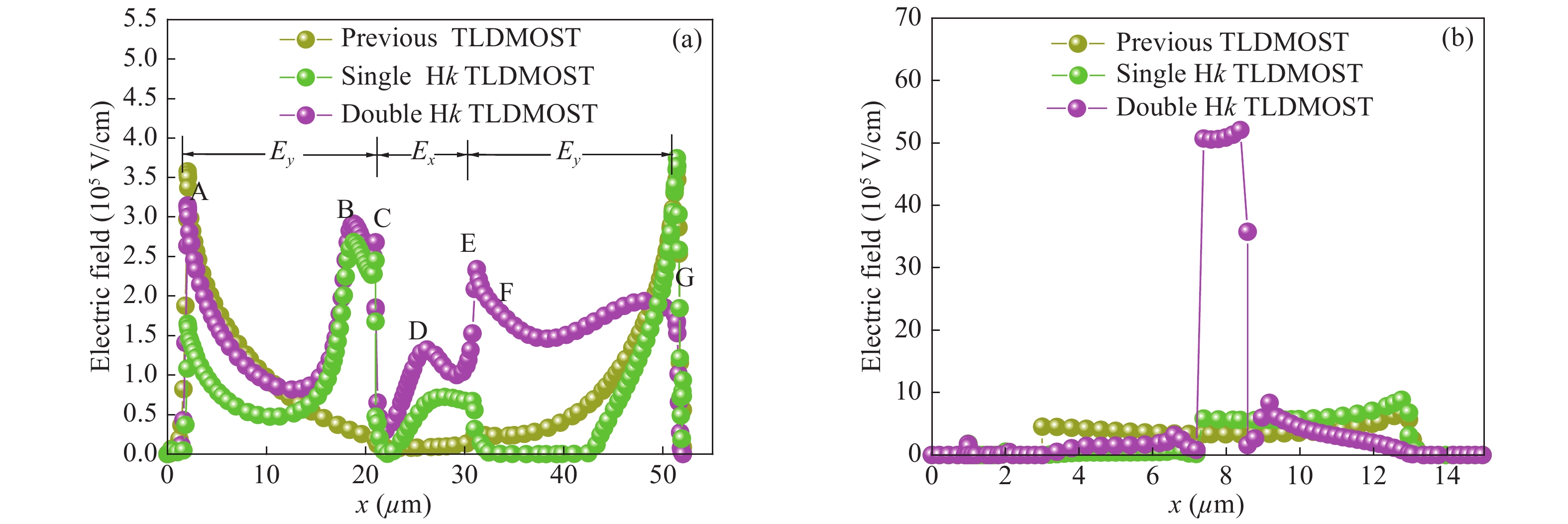
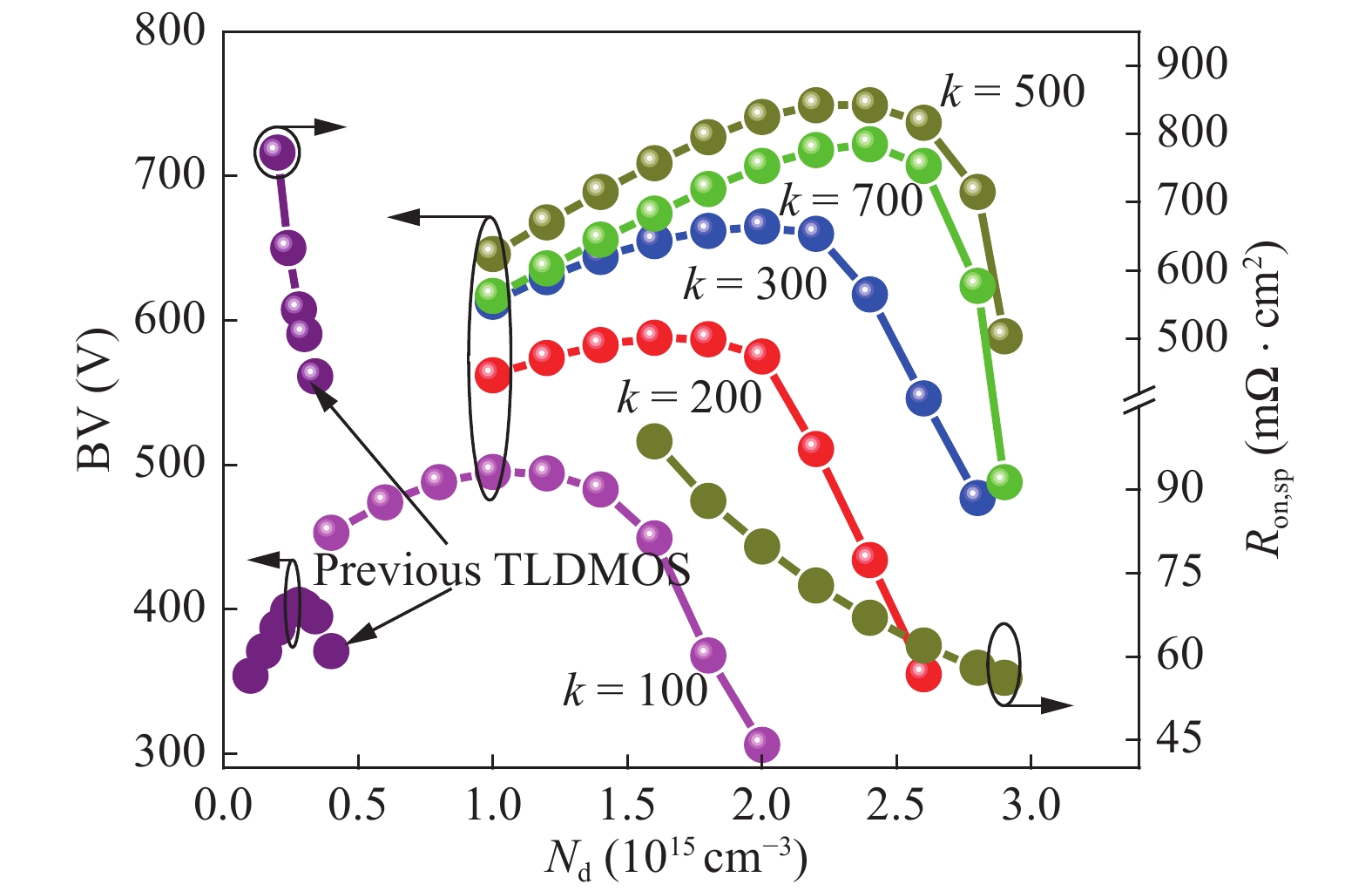
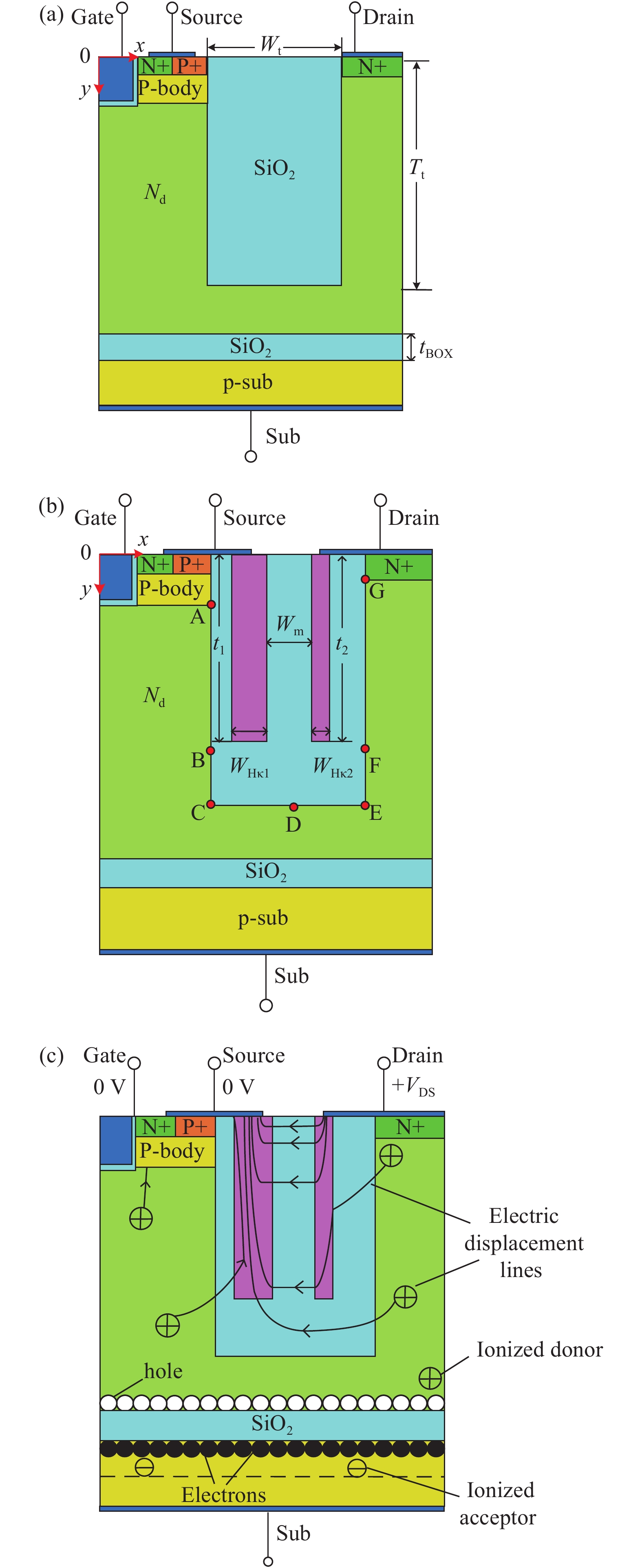
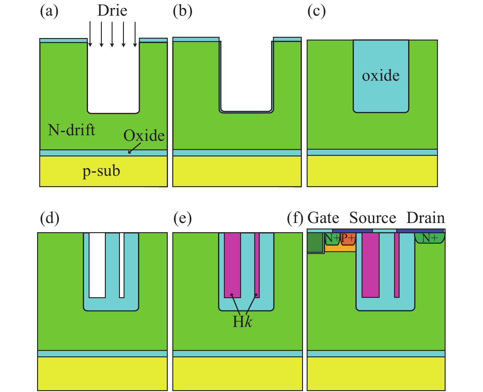
Abstract: An SOI trench LDMOST (TLDMOST) with ultra-low specific on-resistance (Ron,sp) is proposed. It features double vertical high-k insulator pillars (Hk1 and Hk2) in the oxide trench, which are connected to the source electrode and drain electrode, respectively. Firstly, under reverse bias voltage, most electric displacement lines produced by the charges of the depleted drift region in the source side go through the Hk1, and thus the average electric field strength under the source can be enhanced. Secondly, two additional electric field peaks are induced by the Hk1, which further modulate the electric field in the drift region under the source. Thirdly, most electric displacement lines produced by the charges of the depleted drift region in the drain side enter into the Hk2. This not only introduces one more electric field peak at the corner of the oxide trench around the Hk2, but also forms the enhanced vertical reduced surface field effect, which modulates the electric field in the drift region under the drain. With the effects of the two Hk insulator pillars, the breakdown voltage (BV) and the drift region doping concentration are significantly improved. The simulation results indicate that compared with the oxide trench LDMOST (previous TLDMOST) with the same geometry, the proposed double Hk TLDMOST enhances the BV by 86% and reduces the Ron,sp by 88%.

Key words: breakdown voltagehigh-kspecific on-resistancetrench LDMOST

The lateral double diffused metal–oxide–semiconductor transistor (LDMOST) has been widely used in smart power integrated circuits (SPIC). The main design target of LDMOSTs is the trade-off between specific on-resistance (Ron,sp) and breakdown voltage (BV), which remains a large challenge to the development and application of high voltage LDMOSTs[1].

Normally, a higher BV requires a longer drift region length and a lower drift region doping concentration, which lead to a higher Ron,sp. The reduced surface field (RESURF) technique has been widely employed in LDMOST to realize a high BV. However, the BV of the RESURF LDMOST is very sensitive to the deviation of the voltage-sustaining region doping from the optimized value, and the Ron,sp is still high due to the long drift region with limited doping dose in it. The trench technique has been proved to effectively reduce the cell pitch by inserting an oxide trench in the drift region and thus reduce the Ron,sp without sacrificing the BV[24]. Combining with the superjunction technique, a deep trench SOI LDMOST in Ref. [5] has achieved a significant improvement of the trade-off, but the BV is still greatly affected by the deviation of the voltage-sustaining region doping. In Ref. [6], a device with N/P pillars and field plates was reported to further improve the static performance. For this device, a high gate capacitance CGD is induced by the vertical gate field plate and thus increases the gate driving loss. High-k dielectrics (Hk) are usually used as the gate dielectric in microelectronic devices[711]. Besides, the device using Hk and Si as a compound voltage-sustaining region was proposed to improve the trade-off and achieve less sensitivity of charge imbalance[1215].

In this paper, an improved SOI trench LDMOST utilizing the double vertical Hk pillars (double Hk TLDMOST) is proposed for the first time. In the proposed TLDMOST, two Hk pillars, which are vertically inserted in the oxide trench, assist in depleting the drift region, and thus both the average electric field strengths in the drift region and the deep trench are enhanced. An ultra-low Ron,sp is achieved for the two Hk pillars to assist in depleting the drift region, and the drift region doping concentration could be increased. Therefore, the trade-off between the BV and Ron,sp can be significantly improved. In the following sections, the structure, the mechanism and the performance will be studied in detail.

Figs. 1(a) and 1(b) show the structures of the previous and proposed TLDMOSTs, respectively. In the proposed structure, the double Hk pillars, Hk1 and Hk2, are vertically inserted in the oxide trench, and connected to the source and the drain electrodes, respectively. The t1 and t2 represent the thicknesses of Hk1 and Hk2, respectively. The WHk1 and WHk2 denote the widths of Hk1 and Hk2, respectively. The Tt and Wt are the thickness and width of the deep trench, respectively. The tBOX and tox are the thicknesses of the buried oxide (BOX) layer and gate oxide, respectively. The Nd is the doping concentration of the drift region.

Fig. 1(c) illustrates the mechanism of the proposed double Hk TLDMOST under reverse bias. As for the vertical blocking voltage, the BV is determined by the maximum voltage drop across the SOI layer and BOX. By virtue of the back-gate effect, the holes and electrons are simultaneously accumulated on the opposite side of the BOX, which induce the additional electric field and significantly increase the total value in the BOX according to the Gauss’s law.

As for the lateral blocking voltage, the BV is influenced by both the path AG across the trench and the path ABCDEFG (A–G) around the trench, shown in Fig. 1(b). Considering the high critical electric field (Ec) of the insulator (e.g., Ec > 6 × 10 6 V/cm for SiO2, and Ec > 1 × 10 6 V/cm for SrTiO3[16]), the breakdown hardly occurs in the trench. Therefore, the BV is mainly determined by the maximum voltage drop along the path A–G.

In the TLDMOST with single Hk pillar, Hk1, inserted in the oxide trench (single Hk TLDMOST), since the permittivity of the Hk1 is supposed to be much higher than that of the Si[1214], most electric displacement lines produced by the positive charges in the drift region and N+ drain region go through the Hk1 instead of the Si, and terminate at the source electrode. This can be explained by comparing a static electric field to a current field[12]. Compared with the drift region, the Hk1 has a much higher conductivity, and it is obvious that a large portion of the current flows in the Hk1. This makes only a few of the ionized donors in the drift region contribute to the electric field of the p-body/n-drift junction. Therefore, heavier doping concentration can be used in the drift region without producing a high electric field at the p-body/n-drift junction, and the improved average electric field in the drift region under the source can be achieved. However, in the drain side, a large amount of the electric displacement lines produced by ionized donors in the N+ drain region tend to gather at the drain side, causing a sharp increase of the electric field at the N+ drain side and a premature breakdown occurs.

To improve the electric field distribution under the drain, a second Hk pillar (Hk2) connected to the drain electrode is introduced. Most of the electric displacement lines produced by the ionized impurities under the drain are via the Hk2 with high conductivity, spread toward the bottom of the Hk2, and finally terminate at the source electrode. This not only relaxes the gathering of electric displacement lines at the N+ drain, but also enhances the average electric field along the path E–G. From the above analysis, it is convincing that the proposed TLDMOST has a higher BV and a heavier Nd as well by comparing with the previous TLDMOST with the same geometry.

The performances of the proposed TLDMOST are investigated and optimized by MEDICI[17]. The models of CONMOB, SRH, AUGER, FLDMOB, and IMPACT.I are used in the simulations. The key simulation parameters are as follows: t1 = t2 = 18 μm, tBOX = 1 μm, tox = 30 nm, Tt = 21 μm, WHk1 = 3.2 μm, WHk2 = 1 μm, Wm=1.4 μm, Wt = 10 μm, and the thickness of the SOI layer is 25 μm.

Fig. 2 shows the potential contours of the proposed double Hk, single Hk and previous TLDMOSTs at breakdown. In Fig. 2(a), the double Hk TLDMOST exhibits a uniform potential distribution and realizes a high BV of 749 V. The single Hk TLDMOST suffers from a low electric field in the drift region under the drain. This is attributed to the amounts of electric displacement lines gathering at the point G owing to a high curvature, causing a high electric field and a premature breakdown at the point G. However, in Fig. 2(c), the very sparse equipotential contours in the lower section of the drift region under both the source and the drain are shown in the previous TLDMOST and correspond to a poor BV of 403 V.

Figure  2.  (Color online) Potential contours of (a) double Hk, (b) single Hk and (c) previous TLDMOSTs at breakdown (10 V/div, Nd = 2.4 × 1015 cm−3 for double Hk and single Hk TLDMOSTs, Nd = 2.8 × 1014 cm−3 for previous TLDMOST).

Fig. 3(a) illustrates the electric field distributions around the oxide trench of the three TLDMOSTs. Due to the electric field modulation by the Hk1 and Hk2, it is obvious that four new electric field peaks are introduced at the points B, C, D, and E, whereas the electric fields at the corresponding points of the previous TLDMOST are very low. The single Hk TLDMOST exhibits a much more uniform electric field in the drift region under the source than that under the drain, as discussed earlier in Section 2. Besides, the electric fields at points A and G, which limit the breakdown voltage of the previous TLDMOST, are significantly reduced in the proposed double Hk TLDMOST. This avoids premature breakdown at the surface.

Figure  3.  (Color online) (a) Electric field distributions around the trench in the previous, single Hk, and double Hk TLDMOSTs at breakdown. (b) The surface electric field distributions of the three TLDMOSTs at breakdown.

Fig. 3(b) shows the surface electric field distributions (y = 0.01 μm) of the double Hk, the single Hk, and the previous TLDMOSTs. The maximum electric field in the insulator trench of the double Hk TLDMOST reaches to 5.1 × 10⁶ V/cm compared with 3.3 × 10⁵ V/cm of the previous TLDMOST, but is still lower than the Ec of the oxide. That is to say, the breakdown will not happen in the deep trench.

According to Ref. [12], the ability for the Hk insulator to transmit the electric displacement is determined by the relative permittivity (k), the width and the thickness of the Hk pillar, which are the key parameters for the breakdown performance. There are some Hk materials which may be possible for the proposed TLDMOST, such as SrTiO3, PZT, PbTe or an insulator with conducting particle. These dielectrics have a value of k in the range of 100–500 or even higher[14, 1820].

Fig. 4 gives the BV and Ron,sp versus Nd in the previous TLDMOST and the proposed one for different values of k. In the proposed TLDMOST, the BV increases first and then decreases with the increase of k value for a given Nd. For example when Nd is 2 × 1015 cm−3, for k = 100, amounts of electric displacement lines produced by the positive charges of the depleted drift region under the source gather at the corner of the trench gate. Thus, the peak electric field there increases, and a premature breakdown occurs. When the permittivity of Hk increases, an increasing number of electric displacement lines produced by the charges mentioned above are absorbed by Hk1. This relaxes the peak electric field at the corner of the trench gate and results in an improvement of BV. However, the electric field at point E increases with the permittivity of Hk2 increasing. When the k value is too large, e.g. 700, a premature breakdown happens at point E.

As illustrated in Fig. 4, there is an optimal value of Nd for a certain value of k. The maximum BV of 749 V can be achieved corresponding to an Ron,sp of 67 mΩ·cm2 for Nd = 2.4 × 1015 cm−3 and k = 500. As a consequence, the BV is enhanced by 86%, and the Ron,sp is reduced by 88% compared with the previous TLDMOST for the same geometry.

Furthermore, as indicated in Fig. 4, the proposed structure is more robust to the deviation of Nd than the previous one. For the latter, the electric displacement lines produced by the depleted N+ drain tend to concentrate at the point G at a value of Nd lower than the optimal value, whereas for the former, the gathering effect is significantly relieved by the Hk2. Accordingly, the electric field peak at the point G is reduced, and the BV has less sensitivity to the Nd. When the Nd is higher than the optimal value, for the previous TLDMOST, the electric displacement lines produced by the ionized donors in the drift region tend to crowd at the p-body/n-drift junction and increase the surface electric field. However, for the proposed structure, most electric displacement lines produced by the aforementioned charges are prone to access the Hk1. This makes only a few of the ionized donors contribute to the electric field of the p-body/n-drift junction. Therefore, the BV has no significant change with the variation of the Nd, compared with the previous TLDMOST.

Figure  4.  (Color online) The BV and Ron,sp versus Nd in previous TLDMOST and the proposed one for different k.

Fig. 5(a) illustrates the influence of t1 and WHk1 on the BV when the t2 = 18 μm and WHk2 = 1 μm. When there is no Hk1, a large amount of electric displacement lines produced by the depleted drift region gather at point A, causing an electric field peak at point A and a premature breakdown. After the Hk1 is applied, a portion of electric displacement lines are absorbed by the Hk1, which causes a new electric field peak at point B shown in Fig. 1(b) and a reduced electric field at point A. With the value of t1 (or WHk1) increasing, the number of electric displacement lines absorbed by the Hk1 increases, and less ionized donors will terminate at the p-body/n-drift junction. Consequently, the electric field peak at the p-body/n-drift junction reduces, and the average electric field in the drift region under the source enhances, both of which suggest a higher BV. Once the value of t1 (or WHk1) is larger than its optimal value, the BV reduces, largely on the grounds that excessive electric displacement lines crowd at point B inducing a high electric field.

Figure  1.  (Color online) Structures of (a) the previous TLDMOST and (b) the proposed TLDMOST, and (c) the schematic diagram of Fig. 1(b) under the blocking state.
Figure  5.  (Color online) (a) The BV versus WHk1 at different values of t1. (b) The BV versus WHk2 at different values of t2.

The influence of t2 and WHk2 on the BV at t1 = 18 μm and WHk1 = 3.2 μm is depicted in Fig. 5(b), revealing that both t2 and WHk2 have significant effects on the electric field distribution in the drift region under the drain. A small t2 or WHk2 induces a high average electric field in the drift region between points G and F, whereas the drift region between points F and E sustains a low voltage drop. On the contrary, a large t2 or WHk2 causes a large voltage drop between points F and E, whereas the average electric field in the drift region between points G and F is reduced, both of which are detrimental to the high BV.

Fig. 6 clearly manifests the dependence of the BV on the Wm at given dimensions of the two Hk pillars. The structure parameters of Hk1 and Hk2 are as follows: t1 = 18 μm, WHk1 = 3.2 μm, t2 = 18 μm, and WHk2 = 1 μm. When the Wm is larger than the optimal value, amounts of the electric displacement lines produced by the depleted drift region under the source are easily absorbed by Hk1, causing a sharp increase of the electric field peak at point B and a premature breakdown occurs. The BV reduces if the Wm is lower than the optimal value. This is owing to the fact that most of the electric displacement lines produced by the aforementioned charge directly enter into the gate electrode, rather than the source electrode via the Hk1, resulting in a high electric field at the corner of the gate.

Figure  6.  (Color online) Influences of the space between Hk1 and Hk2 (Wm) on BV.

Fig. 7 shows the gate charge characteristics of the proposed TLDMOST and the previous TLDMOST, where the inset illustrates the simulation circuit and VDD is set to 200 V. As revealed in the figure, the gate–source charge (QGS) of the proposed TLDMOST remains constant at different values of k, which is approximately identical to that of the previous TLDMOST. The proposed TLDMOST exhibits a gate–drain charge (QGD) of 3.2 × 10⁻¹⁵ C/μm, increased by 55% compared with the previous TLDMOST. The larger QGD is caused by the inserted Hk insulator. However, compared with the trench LDMOS in Ref. [6], the proposed structure exhibits a QGD value reduced by 88%.

Figure  7.  (Color online) Gate charge characteristics of proposed TLDMOST and previous TLDMOST.

Fig. 8 depicts the switching characteristics of the proposed TLDMOST and the previous TLDMOST. The gate resistance is 30 Ω. The drain electrodes of the devices are connected to a VDD of 200 V through a load resistor RL. To obtain the same current density for both the TLDMOSTs, the values of RL are chosen as 6.619 × 10⁷ Ω and 6.2 × 10⁷ Ω, respectively. In the proposed double Hk TLDMOST, with the value of k increasing, both the turn-on time and the turn-off time increase. The rise time of the proposed structure is 1.33 ns at k = 500, which is approximate to that of the previous structure. The fall time of the proposed structure is 60.4 ns, which is 55.4 ns slower than the previous structure. The longer fall time of the proposed TLDMOST is resulted from the added body capacitance CDS by the Hk pillars.

Figure  8.  (Color online) Switching characteristics of the proposed TLDMOST and previous TLDMOST. (a) Turn-on. (b) Turn-off.

Fig. 9 shows the key process steps to fabricate the double Hk TLDMOST. The deep trench can be formed by the DRIE in Fig. 9(a). The dry oxidation of the thin liner oxide is followed in Fig. 9(b) to reduce the interface states near the interface. In Fig. 9(c), the trench is filled with oxide and polished. Trench etching[6, 21, 22] and deposition of the Hk are followed to form the double Hk pillars in Figs. 9(d)9(e). In Fig. 9(f), the remaining process steps including the p-body implantation, gate etch and polysilicon deposition, P+/N+ region implantation, the contact etch, the metal deposition and etch are implemented by using the conventional processes.

Figure  9.  (Color online) Key process steps to fabricate a prototype double Hk device. (a) Trench etching. (b) Dry oxidation. (c) Filling the trench with dielectric and polishing. (d) Etching deep trench. (e) Deposition of High k. (f) Forming the p-body, the polysilicon gate, P+ and N+ by the conventional methods.

This paper has presented an analysis of the specific on-resistance and the breakdown voltage of an improved TLDMOST with double Hk pillars. The double Hk pillars assist depleting the drift region, and modulate the electric field distribution, which lead to the increase of the drift doping concentration. As a consequence, compared with the previous TLDMOST, the proposed structure achieves a better trade-off between the BV and the Ron,sp. The simulation results indicate that the optimized proposed TLDMOST exhibits a BV of 749 V and an Ron,sp of 67 mΩ·cm2 at k = 500, which breaks the silicon limit. Even though the turn-off time of the proposed structure is longer than that of the previous TLDMOST, it is acceptable in most applications that the switching frequency is not very high.


[1]
Qiao M, Wang Z K, Wang Y R, et al. 3-D Edge termination design and Ron,sp-BV model of a 700-V triple RESURF LDMOS with n-type top layer. IEEE Trans Electron Devices, 2017, 64(6): 2579 doi: 10.1109/TED.2017.2694451
[2]
Miao R Y, Lu F, Wang Y Y, et al. Deep oxide trench termination structure for super-junction MOSFET. Electron Lett, 2012, 48(16): 1018 doi: 10.1049/el.2012.2061
[3]
Varadarajan K R, Chow T P, Wang J, et al. 250 V integrable silicon lateral trench power MOSFETs with superior specific on-resistance. Proceedings of the 19th International Symposium on Power Semiconductor Devices and IC’s (ISPSD), 2007: 233
[4]
Lu D H F, Jimbo S, Fujishima N. A low on-resistance high voltage SOI LIGBT with oxide trench in drift region and hole bypass gate configuration. IEEE International Electron Devices Meeting, 2005: 381
[5]
Zhang W T, Qiao M, Wu L J, et al. Ultra-low specific on-resistance SOI high voltage trench LDMOS with dielectric field enhancement based on ENBULF concept. Proceedings of the 25th ISPSD, 2013: 329
[6]
Chao X, Cheng X H, Wang Z J, et al. Improvement of SOI trench LDMOS performance with double vertical metal field plate. IEEE Trans Electron Devices, 2014, 61(10): 3477 doi: 10.1109/TED.2014.2349553
[7]
He G, Chen X S, Sun Z Q. Interface engineering and chemistry of Hf-based high-k dielectrics on III–V substrates. Surf Sci Rep, 2013, 68(1): 68 doi: 10.1016/j.surfrep.2013.01.002
[8]
He G, Deng B, Chen H S, et al. Effect of dimethylaluminumhydride-derived aluminum oxynitride passivation layer on the interface chemistry and band alignment of HfTiO–InGaAs gate stacks. APL Mater, 2013, 1: 012104 doi: 10.1063/1.4808243
[9]
He G, Liu J W, Chen H S, et al. Interface control and modification of band alignment and electrical properties of HfTiO/GaAs gate stacks by nitrogen incorporation. J Mater Chem C, 2014, 2(27): 5299 doi: 10.1039/C4TC00572D
[10]
Zhang J W, He G, Zhou L, et al. Microstructure optimization and optical and interfacial properties modulation of sputtering-derived HfO2 thin films by TiO2 incorporation. J Alloys Comp, 2014, 611: 253 doi: 10.1016/j.jallcom.2014.05.074
[11]
He G, Gao J, Chen H S, et al. Modulating the interface quality and electrical properties of HfTiO/InGaAs gate stack by atomic-layer-deposition-derived Al2O3 passivation layer. ACS Appl Mater Interfaces, 2014, 6(24): 22013 doi: 10.1021/am506351u
[12]
Chen X B, Huang M M. A vertical power MOSFET with an interdigitated drift region using high-k insulator. IEEE Trans Electron Devices, 2012, 59(9): 2430 doi: 10.1109/TED.2012.2204890
[13]
Chen X B. Super-junction voltage sustaining layer with alternating semiconductor and high-k dielectric regions. US Patent, No. 7230310, 2007
[14]
Li J H, Li P, Huo W R, et al. Analysis and fabrication of an LDMOS with high-permittivity dielectric. IEEE Electron Device Lett, 2011, 32(9): 1266 doi: 10.1109/LED.2011.2158383
[15]
Guo Y F, Yao J F, Zhang B, et al. Variation of lateral width technique in SOI high-voltage lateral double-diffused metal–oxide–semiconductor transistors using high-k dielectric. IEEE Electron Device Lett, 2015, 36(3): 262 doi: 10.1109/LED.2015.2393913
[16]
Cai X Y, Frisbie C D, Leighton C. Optimized dielectric properties of SrTiO3 : Nb/SrTiO3 (001) films for high field effect charge densities. Appl Phys Lett, 2006, 89(24): 242915 doi: 10.1063/1.2404610
[17]
User’s Manual of Two-Dimensional Device Simulation Program MEDICI, Version 2001.2, Synopsys MEDICI User’s Manual, Synopsys Inc., Mountain View, CA, USA, 2010
[18]
Naugarhiya A, Kondekar P N. High permittivity material selection for design of optimum Hk VDMOS. Superlatt Microstruct, 2015, 83: 310 doi: 10.1016/j.spmi.2015.02.045
[19]
Chen X B. Surface (lateral) voltage-sustaining region with an insulator film containing conductive particles. US Patent, No. 0175657, 2013
[20]
Yi B, Lin Z, Chen X B. Study on HK-VDMOS with deep trench termination. Superlatt Microstruct, 2014, 83: 278
[21]
Donohue L A, Hopkins J, Barnett R, et al. Developments in Si and SiO2 etching for MEMS-based optical applications. Proc SPIE, 2003, 5347: 44
[22]
Schaepkens M, Oehrlein G S. A review of SiO2 etching studies in inductively coupled fluorocarbon plasmas. J Electrochem Soc, 2001, 148(3): C211 doi: 10.1149/1.1348260
Fig. 2.  (Color online) Potential contours of (a) double Hk, (b) single Hk and (c) previous TLDMOSTs at breakdown (10 V/div, Nd = 2.4 × 1015 cm−3 for double Hk and single Hk TLDMOSTs, Nd = 2.8 × 1014 cm−3 for previous TLDMOST).

Fig. 3.  (Color online) (a) Electric field distributions around the trench in the previous, single Hk, and double Hk TLDMOSTs at breakdown. (b) The surface electric field distributions of the three TLDMOSTs at breakdown.

Fig. 4.  (Color online) The BV and Ron,sp versus Nd in previous TLDMOST and the proposed one for different k.

Fig. 1.  (Color online) Structures of (a) the previous TLDMOST and (b) the proposed TLDMOST, and (c) the schematic diagram of Fig. 1(b) under the blocking state.

Fig. 5.  (Color online) (a) The BV versus WHk1 at different values of t1. (b) The BV versus WHk2 at different values of t2.

Fig. 6.  (Color online) Influences of the space between Hk1 and Hk2 (Wm) on BV.

Fig. 7.  (Color online) Gate charge characteristics of proposed TLDMOST and previous TLDMOST.

Fig. 8.  (Color online) Switching characteristics of the proposed TLDMOST and previous TLDMOST. (a) Turn-on. (b) Turn-off.

Fig. 9.  (Color online) Key process steps to fabricate a prototype double Hk device. (a) Trench etching. (b) Dry oxidation. (c) Filling the trench with dielectric and polishing. (d) Etching deep trench. (e) Deposition of High k. (f) Forming the p-body, the polysilicon gate, P+ and N+ by the conventional methods.

[1]
Qiao M, Wang Z K, Wang Y R, et al. 3-D Edge termination design and Ron,sp-BV model of a 700-V triple RESURF LDMOS with n-type top layer. IEEE Trans Electron Devices, 2017, 64(6): 2579 doi: 10.1109/TED.2017.2694451
[2]
Miao R Y, Lu F, Wang Y Y, et al. Deep oxide trench termination structure for super-junction MOSFET. Electron Lett, 2012, 48(16): 1018 doi: 10.1049/el.2012.2061
[3]
Varadarajan K R, Chow T P, Wang J, et al. 250 V integrable silicon lateral trench power MOSFETs with superior specific on-resistance. Proceedings of the 19th International Symposium on Power Semiconductor Devices and IC’s (ISPSD), 2007: 233
[4]
Lu D H F, Jimbo S, Fujishima N. A low on-resistance high voltage SOI LIGBT with oxide trench in drift region and hole bypass gate configuration. IEEE International Electron Devices Meeting, 2005: 381
[5]
Zhang W T, Qiao M, Wu L J, et al. Ultra-low specific on-resistance SOI high voltage trench LDMOS with dielectric field enhancement based on ENBULF concept. Proceedings of the 25th ISPSD, 2013: 329
[6]
Chao X, Cheng X H, Wang Z J, et al. Improvement of SOI trench LDMOS performance with double vertical metal field plate. IEEE Trans Electron Devices, 2014, 61(10): 3477 doi: 10.1109/TED.2014.2349553
[7]
He G, Chen X S, Sun Z Q. Interface engineering and chemistry of Hf-based high-k dielectrics on III–V substrates. Surf Sci Rep, 2013, 68(1): 68 doi: 10.1016/j.surfrep.2013.01.002
[8]
He G, Deng B, Chen H S, et al. Effect of dimethylaluminumhydride-derived aluminum oxynitride passivation layer on the interface chemistry and band alignment of HfTiO–InGaAs gate stacks. APL Mater, 2013, 1: 012104 doi: 10.1063/1.4808243
[9]
He G, Liu J W, Chen H S, et al. Interface control and modification of band alignment and electrical properties of HfTiO/GaAs gate stacks by nitrogen incorporation. J Mater Chem C, 2014, 2(27): 5299 doi: 10.1039/C4TC00572D
[10]
Zhang J W, He G, Zhou L, et al. Microstructure optimization and optical and interfacial properties modulation of sputtering-derived HfO2 thin films by TiO2 incorporation. J Alloys Comp, 2014, 611: 253 doi: 10.1016/j.jallcom.2014.05.074
[11]
He G, Gao J, Chen H S, et al. Modulating the interface quality and electrical properties of HfTiO/InGaAs gate stack by atomic-layer-deposition-derived Al2O3 passivation layer. ACS Appl Mater Interfaces, 2014, 6(24): 22013 doi: 10.1021/am506351u
[12]
Chen X B, Huang M M. A vertical power MOSFET with an interdigitated drift region using high-k insulator. IEEE Trans Electron Devices, 2012, 59(9): 2430 doi: 10.1109/TED.2012.2204890
[13]
Chen X B. Super-junction voltage sustaining layer with alternating semiconductor and high-k dielectric regions. US Patent, No. 7230310, 2007
[14]
Li J H, Li P, Huo W R, et al. Analysis and fabrication of an LDMOS with high-permittivity dielectric. IEEE Electron Device Lett, 2011, 32(9): 1266 doi: 10.1109/LED.2011.2158383
[15]
Guo Y F, Yao J F, Zhang B, et al. Variation of lateral width technique in SOI high-voltage lateral double-diffused metal–oxide–semiconductor transistors using high-k dielectric. IEEE Electron Device Lett, 2015, 36(3): 262 doi: 10.1109/LED.2015.2393913
[16]
Cai X Y, Frisbie C D, Leighton C. Optimized dielectric properties of SrTiO3 : Nb/SrTiO3 (001) films for high field effect charge densities. Appl Phys Lett, 2006, 89(24): 242915 doi: 10.1063/1.2404610
[17]
User’s Manual of Two-Dimensional Device Simulation Program MEDICI, Version 2001.2, Synopsys MEDICI User’s Manual, Synopsys Inc., Mountain View, CA, USA, 2010
[18]
Naugarhiya A, Kondekar P N. High permittivity material selection for design of optimum Hk VDMOS. Superlatt Microstruct, 2015, 83: 310 doi: 10.1016/j.spmi.2015.02.045
[19]
Chen X B. Surface (lateral) voltage-sustaining region with an insulator film containing conductive particles. US Patent, No. 0175657, 2013
[20]
Yi B, Lin Z, Chen X B. Study on HK-VDMOS with deep trench termination. Superlatt Microstruct, 2014, 83: 278
[21]
Donohue L A, Hopkins J, Barnett R, et al. Developments in Si and SiO2 etching for MEMS-based optical applications. Proc SPIE, 2003, 5347: 44
[22]
Schaepkens M, Oehrlein G S. A review of SiO2 etching studies in inductively coupled fluorocarbon plasmas. J Electrochem Soc, 2001, 148(3): C211 doi: 10.1149/1.1348260
  • Search

    Advanced Search >>

    GET CITATION

    shu

    Export: BibTex EndNote

    Article Metrics

    Article views: 4045 Times PDF downloads: 66 Times Cited by: 0 Times

    History

    Received: 29 December 2017 Revised: 10 February 2018 Online: Uncorrected proof: 17 April 2018Accepted Manuscript: 26 April 2018Published: 01 September 2018

    Catalog

      Email This Article

      User name:
      Email:*请输入正确邮箱
      Code:*验证码错误
      Huan Li, Haimeng Huang, Xingbi Chen. An improved SOI trench LDMOST with double vertical high-k insulator pillars[J]. Journal of Semiconductors, 2018, 39(9): 094009. doi: 10.1088/1674-4926/39/9/094009 ****H Li, H M Huang, X B Chen, An improved SOI trench LDMOST with double vertical high-k insulator pillars[J]. J. Semicond., 2018, 39(9): 094009. doi: 10.1088/1674-4926/39/9/094009.
      Citation:
      Huan Li, Haimeng Huang, Xingbi Chen. An improved SOI trench LDMOST with double vertical high-k insulator pillars[J]. Journal of Semiconductors, 2018, 39(9): 094009. doi: 10.1088/1674-4926/39/9/094009 ****
      H Li, H M Huang, X B Chen, An improved SOI trench LDMOST with double vertical high-k insulator pillars[J]. J. Semicond., 2018, 39(9): 094009. doi: 10.1088/1674-4926/39/9/094009.

      An improved SOI trench LDMOST with double vertical high-k insulator pillars

      DOI: 10.1088/1674-4926/39/9/094009
      Funds:

      Project supported by the National Natural Science Foundation of China (Nos. 51237001, 51607026) and the Fundamental Research Funds for the Central Universities (No. ZYGX2016J048).

      More Information
      • Corresponding author: Email: lile-061022@163.com
      • Received Date: 2017-12-29
      • Revised Date: 2018-02-10
      • Published Date: 2018-09-01

      Catalog

        /

        DownLoad:  Full-Size Img  PowerPoint
        Return
        Return